DOI:
10.1039/C8RA00023A
(Paper)
RSC Adv., 2018,
8, 5721-5727
Efficient multi-barrier thin film encapsulation of OLED using alternating Al2O3 and polymer layers†
Received
2nd January 2018
, Accepted 29th January 2018
First published on 2nd February 2018
Abstract
Organic optoelectronic devices, especially for OLEDs, are extremely susceptibility to water vapor and oxygen which limit their widespread commercialization. In order to extend the shelf-lifetime of devices, thin film encapsulation is the most promising and challenging encapsulation process. In this study, dyad-style multilayer encapsulation structures based on alternating Al2O3 layer and parylene C have been discussed as gas diffusion barriers, in which dense and pinhole-free Al2O3 films were grown by atomic layer deposition (ALD) and flexible parylene C layers were deposited by chemical vapor deposition (CVD). We found the particle in ALD deposited Al2O3 films process is the key killer to barrier property. The thickness of Al2O3 films is the key factor which limit the amount of strain placed on barrier films. With three dyads of the optimal thickness of 30 nm Al2O3 film and 500 nm parylene C, WVTR value is lower than 10−5 g m−2 per day. In addition, the lifetime of OLEDs with and without encapsulation was 190 h and 10 h, respectively. All the results show that this TFE structure has the effective encapsulated property and does not cause degradation of the OLED devices.
Introduction
Flexible organic light-emitting diodes (OLEDs) have received a great deal of attention due to their low manufacturing cost, ease for fabricating large-area products, flexibility and light-weight for integrating with wearable devices.1–6 However, the low work function metallic cathodes and organic materials consisting of OLEDs are highly sensitive to atmospheric moisture and oxygen. Water and oxygen penetrate through plastic substrates to form dark spots and edge shrinkages in OLEDs by oxidizing the as-deposited electrodes or corroding the functional organic layers, resulting in devices degradation, light-output reduction and lifetime decrease.7–12 Accordingly, the requirement of encapsulation technologies is critical to improve the lifetime and reliability of OLEDs. Numerous approaches applied for encapsulation have been developed including the thin film coating, metal lids, glass and the sealing of devices between two glass substrates or plastic substrates treated with barrier films. Among the various candidate counterparties, thin film encapsulation (TFE) is considered as the most promising technology due to its light weight, transparency, and high level of mechanical flexibility.13–19
The barrier performance of inorganic film is the most promising for the development of thin-film encapsulation. However, it is hardly to escape from cracking and pinhole defects in the inorganic layer surface. And also, a thicker inorganic film will introduce the additional risk of cracking under bending, which limit the mechanical flexibility of the encapsulation. Alternating inorganic and organic layer pairs which called Vitex barrier technology currently is the most popular encapsulation solution for flexible devices.20 Inserting the organic layer between inorganic layers leads to improving the flexibility under mechanical deformation.21 Additional, the organic parts can decouple defects existed in inorganic layers, which create a tortuous path to avoid pinholes and cracks that penetrate through the entire encapsulation, result in a very long effective diffusion length lowering the overall permeability.22
Here, we obtain the lowest WVTR (water vapor transmission rate) of optimal high quality single Al2O3 layer film deposited at 60 °C with 20–30 nm thick can reach to 10−4 g m−2 per day. Furthermore, with 3 dyads alternative 30 nm Al2O3 and 500 nm parylene C, the WVTR value of multilayer films can reach to lower than 10−5 g m−2 per day. And the results show that the TFE structure has the effective encapsulated property, and has little effect on the OLED devices. Specifically, we investigated the key parameters affecting the barrier property and flexible stability under mechanical deformation of TFE based on CVD deposited parylene C as organic layers coupling with atomic layer deposited Al2O3 as inorganic layer under a low temperature. We use three dyads of parylene C/Al2O3 optimized films achieved high barrier performance. We also discussed the relationship between barrier performance and flexibility with different thickness of Al2O3 layers. Finally, we studied the thin film encapsulation of OLEDs with parylene C/Al2O3 barrier layers.
Experimental
Preparations of Al2O3 barrier films
The barrier film was consisted of Al2O3 and parylene C pairs. Al2O3 were fabricated by ALD (Savannah-100, Cambridge Nanotech), depositing at 60 °C, which was compatible with organic devices, using sequential, self-limiting exposures to trimethylaluminum (TMA) and water vapor (H2O). The process was that a 0.015 s TMA exposure, a 30 s nitrogen (N2) purge, a 0.015 s of water exposure, and another 30 s nitrogen purge. One cycle above produces an approximately 0.1 nm thick Al2O3 film, so the thickness of the deposited film is controlled by number of cycles. For example, 500 cycles are needed to deposit 50 nm thick Al2O3, which corresponds to 8.5 hours. The thickness of the ALD film was further measured by surface profiler (DEKTAK XT, Bruker). The results indicated that standard deviation was lower than 1%.
Preparations of parylene C layers
The parylene C thin-films were prepared by chemical vapor-phase deposition and polymerization of pary-xylylene in Speciality Coating System (Penta Technology, Suzhou). As shown in Fig. 1, parylene dimers were loaded in the quartz tubular CVD and its vapor converted to a monomer vapor around 680 °C under mechanical pump vacuum. The monomer vapor goes into a chamber then spontaneous polymerization and deposition on the surfaces of all objects including the substrates at room temperature. The deposition rate and thickness of parylene C was monitored online with quartz crystal microbalance monitors. Typically, it was deposited at a rate of 0.1 nm s−1. Parylene C was chosen as the organic layer for dyads barriers to relax the stress of inorganic layers due to the flexible polymer has low modulus (about 4 GPa) and relatively hydrophobic nature. Additional, it can deposit at room temperature without any curing process. Also, it was reported that parylene C can keep water from condensing on the Al2O3 films which is known to corrode Al2O3.23
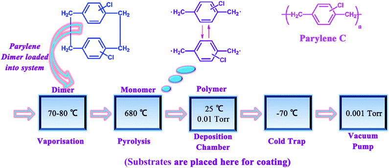 |
| | Fig. 1 Process flow diagram of parylene C coating. | |
OLED device fabrication and encapsulation
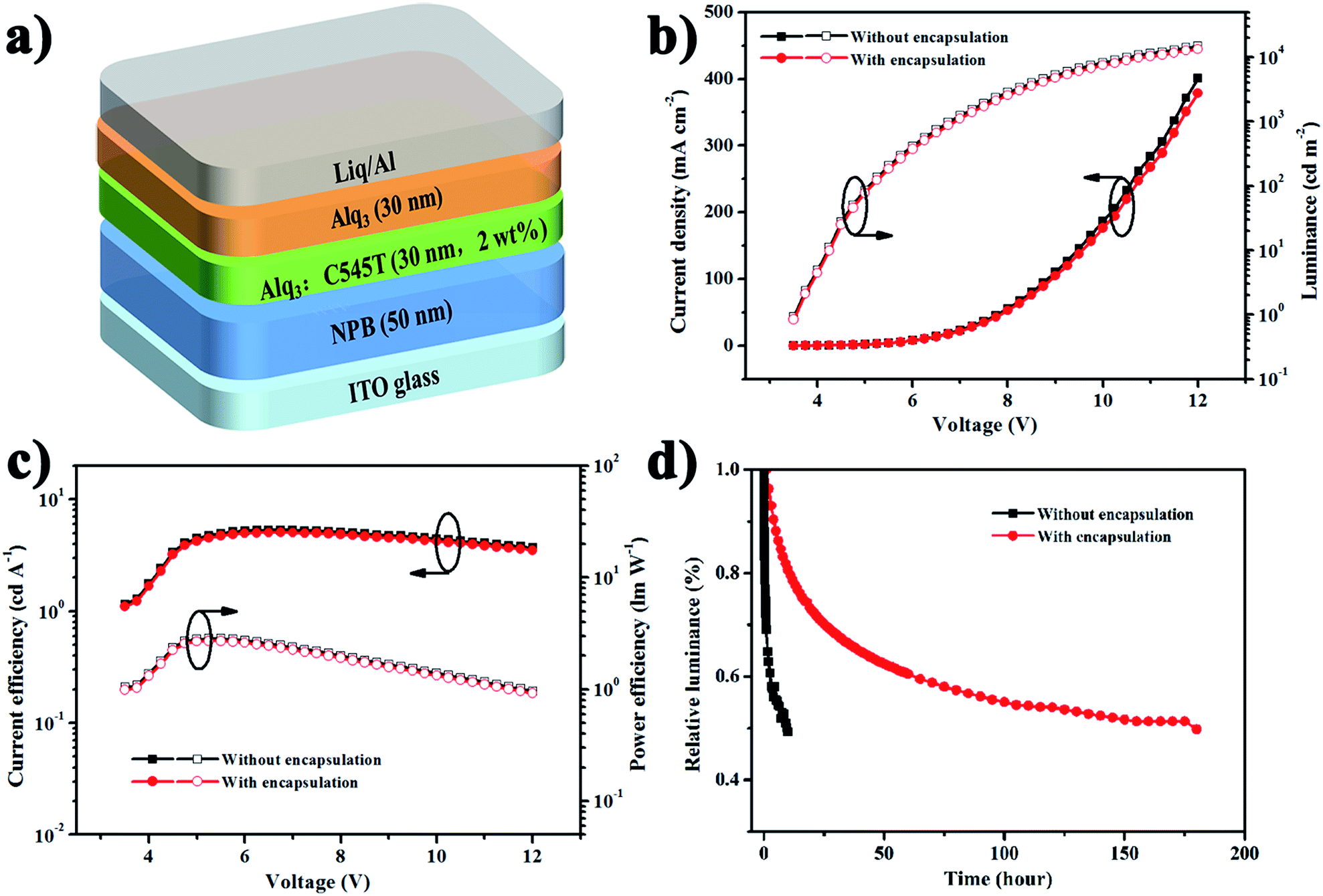
OLEDs were fabricated by thermal evaporation system under a vacuum of less than 10−5 Pa. An ITO (10 ohm □−1, 150 nm)-coated glass substrate was used as anode and cleaned with a detergent solution, deionized water, and acetone. After treated for 3 min by oxygen plasma, the substrate was transferred to vacuum deposition system. The OLEDs were fabricated by sequentially depositing the following organic layer, which were α-naphthylphenylbiphenyl (NPB, 50 nm) as a hole transport layer, tris-(8-quinolato) aluminium (Alq3)![[thin space (1/6-em)]](https://www.rsc.org/images/entities/char_2009.gif) :10-(2-benzothiazolyl)-2,3,6,7-tetrahydro-1,1,7,7-tetramethyl-1H,5H,11H-(1)-benzopyropyrano(6,7-8-i,j)quinolizin-11-one 2% doped (C545T) (30 nm) as a light emitting layer, Alq3 (30 nm) as an electron transport layer, quinolato lithium (Liq, 2 nm) and aluminium (Al) as electron injection layer and cathode, respectively, were evaporated onto the organic layer using a metal shadow mask. Then, an inorganic–organic multilayer barrier film was deposited for TFE. The device performance was measured with a Spectra Scan PR655 and a computer-controlled Keithley 2400 Sourcemeter. All of the devices have an emitting area of 2 × 2 mm2 and measure the luminance only in the forward direction. The lifetime of OLED was measured with a lifetime tester (Polaronix M6000) at an initial luminance of 1000 cd m−2 using constant current mode.
:10-(2-benzothiazolyl)-2,3,6,7-tetrahydro-1,1,7,7-tetramethyl-1H,5H,11H-(1)-benzopyropyrano(6,7-8-i,j)quinolizin-11-one 2% doped (C545T) (30 nm) as a light emitting layer, Alq3 (30 nm) as an electron transport layer, quinolato lithium (Liq, 2 nm) and aluminium (Al) as electron injection layer and cathode, respectively, were evaporated onto the organic layer using a metal shadow mask. Then, an inorganic–organic multilayer barrier film was deposited for TFE. The device performance was measured with a Spectra Scan PR655 and a computer-controlled Keithley 2400 Sourcemeter. All of the devices have an emitting area of 2 × 2 mm2 and measure the luminance only in the forward direction. The lifetime of OLED was measured with a lifetime tester (Polaronix M6000) at an initial luminance of 1000 cd m−2 using constant current mode.
Results and discussion
Multilayer film structure optimization
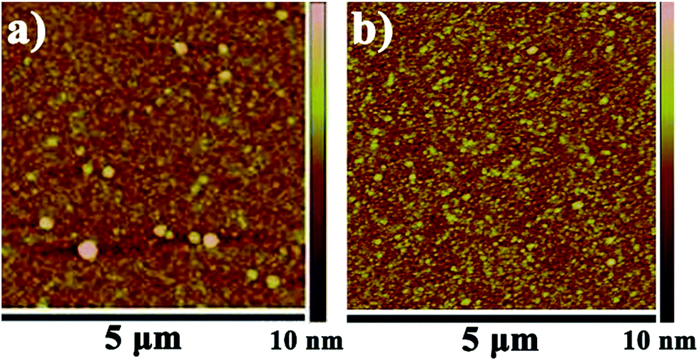
Fig. 2 shows the surface topography of Al2O3 films with different quality on the silicon wafer substrate which was measured by atomic force microscopy (AFM, Veeco, USA). Based upon the AFM images, the principal particle defect structure of the films can be easily detected especially in Fig. 2a. This mainly attributed to the higher base pressure. In Fig. 2a, the base pressure was at 9 × 10⁻¹ torr while it was 2 × 10⁻¹ torr in Fig. 1b. In higher pressure, the slow pumping made the redundant precursor remain in the interface or vapor phase atmosphere rather than purge out immediately in the same purge time and temperature. So, the deposition process was combined ALD with CVD process, which was easy to generate large particles. Obviously, large particles are fatal which would provide paths for the unhindered permeation of water vapor and oxygen, and seriously affect the barrier performance. Additionally, it is well accepted that activation energy of oxygen and water vapor through the fabricated film is strongly dependent on the film quality.24,26 In Fig. 2b, with improving the vacuum, the problem can be well solved. It was shown that large particle was eliminated, and the roughness has reduced from 0.5 nm to 0.3 nm.
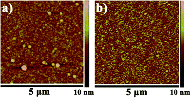 |
| | Fig. 2 AFM topographical images of (a) poor quality Al2O3 (Ra = 0.5 nm) (b) high quality Al2O3 with a thickness of 50 nm (Ra = 0.3 nm) of thin film. | |
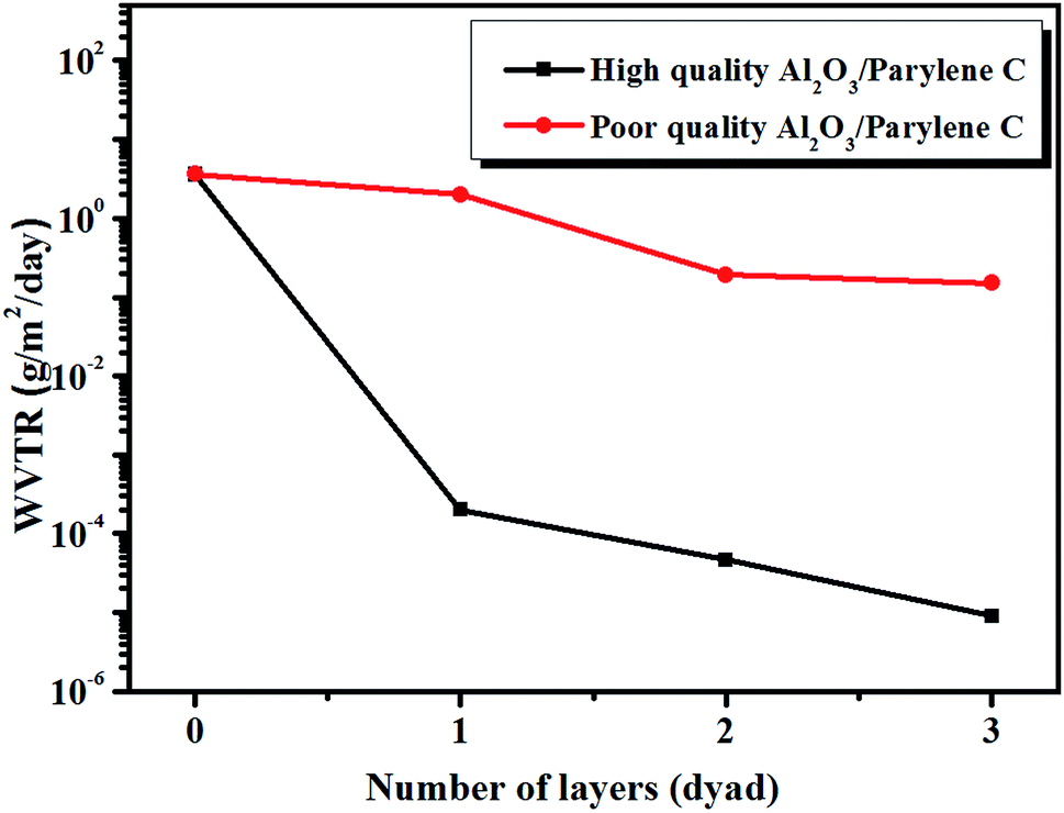
The two kinds of films were respectively used as inorganic layers in the inorganic–organic multilayer encapsulation structures to further investigate the influence of barrier property by WVTR (water vapor transmission rate, Mocon Aquatran II, USA) test. MOCON Aquatran II instrument employs a coulometric sensor to detect the amount of water which penetrates from the coating PET (polyethylene terephthalate). This instrument has a WVTR sensitivity limit of 5 × 10⁻⁵ g m−2 per day at 38 °C/100% relative humidity (RH).25 The primal thickness of Al2O3 was chosen as 50 nm, and the thickness of parylene C was 500 nm. As shown in Fig. 3, the barrier property of multilayer films with high quality Al2O3 layer was significantly superior to the ones of poor quality Al2O3 layer by 2–4 orders of magnitude. Therefore, it is crucial to investigate the surface topography characteristics of inorganic layers in order to obtain high quality films.
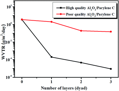 |
| | Fig. 3 Effective WVTR as a function of the number of dyads for Al2O3/parylene C. | |
Except for the influence of film quality, the thickness of Al2O3 films is also a very important parameter for barrier property and flexibility. To obtain the optimal thickness of Al2O3 films, a series of high quality Al2O3 films from 15 nm to 60 nm has been deposited on flexible PET substrates, respectively. As shown in Table 1, the practical barrier performance of single inorganic layer is limited. With the increasing of thickness, the WVTR results reduced firstly and then increased. The firstly reducing with increasing thickness indicates that gradual coverage of Al2O3 films on the PET substrate. But when the thickness reached to 50 nm, the barrier property even got worse. This is because slight deformation and local bending with low strain is unavoidable existing in our experiment and WVTR measurement process, especially with flexible substrate. The thicker coatings in flexible substrates have lower tensile strength and are under less compressive strength due to stress induced cracking, which explained that the worse property with 50 nm and 60 nm Al2O3.26 Therefore, the optimal thickness of Al2O3 films in our experiment is 20–30 nm in order to obtain high barrier property.
Table 1 Effective WVTR of Al2O3 with different thickness
| Sample |
Thickness (nm) |
WVTR (g m−2 per day) |
| 1 |
15 |
6.7 × 10⁻³ |
| 2 |
20 |
0.7 × 10⁻³ |
| 3 |
30 |
0.8 × 10⁻³ |
| 4 |
50 |
1.3 × 10⁻³ |
| 5 |
60 |
4.7 × 10⁻³ |
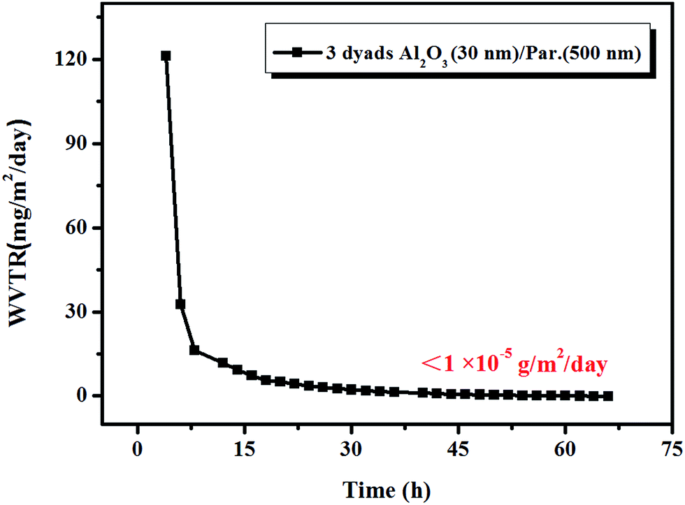
According to above results, the lowest WVTR of optimal high quality inorganic film with 20–30 nm thickness can reach to 10−4 g m−2 per day. However, this value is far away from the need of OLED encapsulation (10−6 g m−2 per day). In order to further improve barrier property and production efficiency, the effective way is applying alternative inorganic–organic multilayer structure. Here we apply parylene C film as organic layer. As shown in Fig. 4, with 3 dyads alternative 30 nm Al2O3 and 500 nm parylene C, the WVTR value of multilayer films can reach to lower than 10−5 g m−2 per day, which exceeds the detect limit of the Mocon Aquatran II and meet the need of OLED encapsulation. With the introduction of organic layers, firstly it helps with stress relaxation during the fabrication of inorganic layer. This obviously enhanced the flexibility of films which can undergo certain deformation and bending. Secondly, it interrupts defects which span the entire thickness of the individual inorganic layers, which creates a tortuous path resulting in very long effective diffusion pathways to reduce the diffusion and permeation rate.27 Last but not the least, the hydrophobic property of parylene C can keep water vapor away from corroding Al2O3 films to enhance the stability of films. Fig. 5 shows a scanning electron microscopy (SEM) cross-sectional image of an Al2O3/parylene C film. Cross-sections were obtained by focused ion beam (FIB) cutting. The SEM image showed that each layer was well-defined, and that delamination at the interface or the presence of defects was scarce.
 |
| | Fig. 4 Effective WVTR of 3 dyads for Al2O3 (30 nm)/parylene C (500 nm). | |
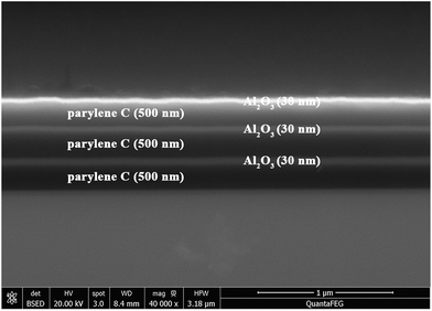 |
| | Fig. 5 SEM image shows cross-section of organic/inorganic multilayer structure. Bright films are 30 nm-thick Al2O3 and dark films are 500 nm-thick parylene. | |
Mechanical property characterization of multilayer films
The mechanical property characterization of multilayer films was to deposit various coatings on the 20% pre-strain PDMS films. The various coatings were separately deposited with 4 dyads 15 nm Al2O3/250 nm parylene C, 2 dyads 30 nm Al2O3/500 nm parylene C and 2 dyads 50 nm Al2O3/500 nm parylene C. After deposition, the pre-strain PDMS films with coatings were elastically recovered to original length, then repeatedly stretched and recovered 10 times but without exceed 20% pre-strain length. In the process of stretching and recovering, the coatings on PDMS need to afford micro-deformation with micron sized curvature radius. In Table 2, it can be clearly seen with the increasing thickness of Al2O3, the flexibility gradually deteriorated. The thinner the thickness of the Al2O3, the smaller the radius of curvature of the bendable deformation that can be sustained. As for initial WVTR, the structure with 2 dyads 30 nm Al2O3/500 nm parylene C has the best property, which is consistent with previous results. Because the initial WVTR of multilayers is dominated by the barrier property of Al2O3 layers. And in Fig. S1,† the cracks and wrinkles in coatings with the three structures can be more intuitively discovered with photos of confocal laser scanning microscope.
Table 2 Change of WVTR with stretching and recovering process of various coating on pre-strain PDMS
| Coatings |
Initial WVTR (g m−2 per day) |
Final WVTR (g m−2 per day) |
Rising rate (%) |
| 4 dyads 15 nm Al2O3/250 nm parylene C |
5.4 |
8.2 |
51.9 |
| 2 dyads 30 nm Al2O3/500 nm parylene C |
1.1 |
3.8 |
254 |
| 2 dyads 50 nm Al2O3/500 nm parylene C |
1.5 |
9.3 |
534 |
Thin film encapsulation of OLED
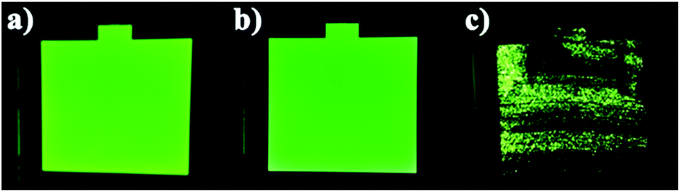
Finally, we adopted the optimal multilayer structure 3 dyads alternative 30 nm Al2O3 and 500 nm parylene C as TFE for OLED encapsulation. In the process of OLED encapsulation, an Al2O3 layer deposited by ALD at 60 °C as the first layer to immediately contact the devices, which can be more effective to avoid the influence of water vapor existing in atmosphere. The absorption of water vapor monomer on the surface of OLED can be reactive with the first TMA pulse in the ALD process. Furthermore, there is less chance for the side permeation of water vapor and oxygen, because in the multilayer structure, parylene C is hydrophobic and the side can be covered by Al2O3 layer by ALD process. And the electroluminescence characteristics and the lifetime of OLED with or without encapsulation have been investigated. In Fig. 6b and c, the device performance of the multilayer thin film encapsulated OLED are identical to those without encapsulation. Additionally, the maximum luminance of 13284 cd m−2 and current efficiency of 5.0 cd A−1 have been obtained in encapsulated OLED. In Fig. 6d, the lifetime of OLED with and without encapsulation was 190 h and 10 h, respectively. Consequently, there is no obvious difference between Fig. 7a (immediately test without TFE) and Fig. 7b (test in two weeks after TFE). But in Fig. 7c the device is test after two days without TFE, and it is corroded with so many dark dots. Now the OLED devices in Fig. 7b has been continue to be lit for more than 1000 h. So, the main reason for the lifetime decrease of the device is the organic material deterioration or interface problem rather than the erosion of water and oxygen. These results show that the TFE structure has the effective encapsulated property, does not harm the OLED devices and is therefore compatible with these devices.
 |
| | Fig. 6 (a) OLED structure diagram, (b) J–V–L, (c) CE–V–PE, (d) lifetime of the OLED without encapsulation and with thin film encapsulation. | |
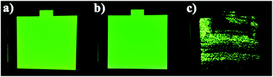 |
| | Fig. 7 OLED brightness images (a) without encapsulation (b) under encapsulation for two weeks (c) without encapsulation for two days. | |
Conclusions
In summary, we proved the superiority of dyad-style multilayer encapsulation structures based on alternating Al2O3 layer and parylene C layer for OLED encapsulation. And in this work, we mainly focused on discussing the influence of large particles existing in Al2O3 films for barrier property, and thickness of Al2O3 films at the effect on flexibility and stability. And the introduction of parylene C films can further enhance the barrier property with a lower WVTR of 10−6 g m−2 per day which is sufficient for protecting the shelf-lifetime of OLED devices. The electroluminescence characteristics of the multilayer thin film encapsulated OLED are identical to those without encapsulation. And the lifetime of OLED with and without encapsulation was 190 h and 10 h, respectively. And the OLED with 3 dyads alternative 30 nm Al2O3 and 500 nm parylene C encapsulation structure has been lit for more than 1000 h. All the results show that this TFE structure has the effective encapsulated property and does not cause degradation of the OLED devices. Due to the encapsulation, the main reason for the lifetime decrease of the device is the organic material deterioration or interface problem rather than the erosion of water and oxygen. Therefore, we obtained a compatible and effective TFE technology to successfully apply for OLED device encapsulation.
Conflicts of interest
There are no conflicts to declare.
Author contributions
The manuscript was written through contributions of all authors. All authors have given approval to the final version of the manuscript.
Acknowledgements
This work was supported by National Program on Key Research Project (2016YFB0401600), the Strategic Priority Research Program of the Chinese Academy of Sciences (XDA09020201), National Natural Science Foundation of China (U1605244).
References
- J. H. Burroughes, D. D. C. Bradley, A. R. Brown, R. N. Marks, K. Mackay, R. H. Friend, P. L. Burn and A. B. Holmes, Light-Emitting-Diodes Based on Conjugated Polymers, Nature, 1990, 347, 539–541 CrossRef CAS.
- G. Gu, V. Bulovic, P. E. Burrows, S. R. Forrest and M. E. Thompson, Transparent organic light emitting devices, Appl. Phys. Lett., 1996, 68, 2606–2608 CrossRef CAS.
- P. E. Burrows, S. R. Forrest and M. E. Thompson, Prospects and applications for organic light-emitting devices, Curr. Opin. Solid State Mater. Sci., 1997, 2, 236–243 CrossRef CAS.
- A. Kraft, A. C. Grimsdale and A. B. Holmes, Electroluminescent conjugated polymers – seeing polymers in a new light, Angew. Chem., Int. Ed., 1998, 37, 402–428 CrossRef.
- S. Kim, H. J. Kwon, S. Lee, H. Shim, Y. Chun, W. Choi, J. Kwack, D. Han, M. Song, S. Kim, S. Mohammadi, I. Kee and S. Y. Lee, Low-Power Flexible Organic Light-Emitting Diode Display Device, Adv. Mater., 2011, 23, 3511–3516 CrossRef CAS PubMed.
- T. H. Han, Y. Lee, M. R. Choi, S. H. Woo, S. H. Bae, B. H. Hong, J. H. Ahn and T. W. Lee, Extremely efficient flexible organic light-emitting diodes with modified graphene anode, Nat. Photonics, 2012, 6, 105–110 CrossRef CAS.
- L. M. Do, E. M. Han, Y. Niidome, M. Fujihira, T. Kanno, S. Yoshida, A. Maeda and A. J. Ikushima, Observation of Degradation Processes of Al Electrodes in Organic Electroluminescence Devices by Electroluminescence Microscopy, Atomic Farce Microscopy, Scanning Electron-Microscopy, and Anger Electron-Spectroscopy, J. Appl. Phys., 1994, 76, 5118–5121 CrossRef CAS.
- J. McElvain, H. Antoniadis, M. R. Hueschen, J. N. Miller, D. M. Roitman, J. R. Sheats and R. L. Moon, Formation and growth of black spots in organic light-emitting diodes, J. Appl. Phys., 1996, 80, 6002–6007 CrossRef.
- D. G. J. Sutherland, J. A. Carlisle, P. Elliker, G. Fox, T. W. Hagler, I. Jimenez, H. W. Lee, K. Pakbaz, L. J. Terminello, S. C. Williams, F. J. Himpsel, D. K. Shuh, W. M. Tong, J. J. Jia, T. A. Callcott and D. L. Ederer, Photo-oxidation of electroluminescent polymers studied by core-level photoabsorption spectroscopy, Appl. Phys. Lett., 1996, 68, 2046–2048 CrossRef CAS.
- H. Aziz, Z. Popovic, C. P. Tripp, N. X. Hu, A. M. Hor and G. Xu, Degradation processes at the cathode/organic interface in organic light emitting devices with Mg:Ag cathodes, Appl. Phys. Lett., 1998, 72, 2642–2644 CrossRef CAS.
- H. Aziz, Z. Popovic, S. Xie, A. M. Hor, N. X. Hu, C. Tripp and G. Xu, Humidity-induced crystallization of tris (8-hydroxyquinoline) aluminum layers in organic light-emitting devices, Appl. Phys. Lett., 1998, 72, 756–758 CrossRef CAS.
- M. Schaer, F. Nuesch, D. Berner, W. Leo and L. Zuppiroli, Water vapor and oxygen degradation mechanisms in organic light emitting diodes, Adv. Funct. Mater., 2001, 11, 116–121 CrossRef CAS.
- E. Langereis, M. Creatore, S. B. S. Heil, M. C. M. Van de Sanden and W. M. M. Kessels, Plasma-assisted atomic layer deposition of Al2O3 moisture permeation barriers on polymers, Appl. Phys. Lett., 2006, 89, 081915 CrossRef.
- A. A. Dameron, S. D. Davidson, B. B. Burton, P. F. Carcia, R. S. McLean and S. M. George, Gas diffusion barriers on polymers using multilayers fabricated by Al2O3 and rapid SiO2 atomic layer deposition, J. Phys. Chem. C, 2008, 112, 4573–4580 CAS.
- J. Meyer, P. Gorrn, F. Bertram, S. Hamwi, T. Winkler, H. H. Johannes, T. Weimann, P. Hinze, T. Riedl and W. Kowalsky, Al2O3/ZrO2 Nanolaminates as Ultrahigh Gas-Diffusion Barriers-A Strategy for Reliable Encapsulation of Organic Electronics, Adv. Mater., 2009, 21, 1845–1849 CrossRef CAS.
- S. Park, W. M. Yun, L. H. Kim, S. Park, S. H. Kim and C. E. Park, Inorganic/organic multilayer passivation incorporating alternating stacks of organic/inorganic multilayers for long-term air-stable organic light-emitting diodes, Org. Electron., 2013, 14, 3385–3391 CrossRef CAS.
- W. Xiao, D. Yu, S. F. Bo, Y. Y. Qiang, Y. Dan, C. Ping, D. Y. Hui and Z. Yi, The improvement of thin film barrier performances of organic-inorganic hybrid nanolaminates employing a low-temperature MLD/ALD method, RSC Adv., 2014, 4, 43850–43856 RSC.
- M. Li, D. Y. Gao, S. Li, Z. W. Zhou, J. H. Zou, H. Tao, L. Wang, M. Xu and J. B. Peng, Realization of highly-dense Al2O3 gas barrier for top-emitting organic light-emitting diodes by atomic layer deposition, RSC Adv., 2015, 5, 104613–104620 RSC.
- L. Wang, C. P. Ruan, M. Li, J. H. Zou, H. Tao, J. B. Peng and M. Xu, Enhanced moisture barrier performance for ALD-encapsulated OLEDs by introducing an organic protective layer, J. Mater. Chem. C, 2017, 5, 4017–4024 RSC.
- L. Moro, T. A. Krajewski, N. M. Rutherford, O. Philips and R. J. Visser, Process and design of a multilayer thin film encapsulation of passive matrix OLED displays, Proc. Soc. Photo-Opt. Instrum. Eng., 2004, 5214, 83–93 CrossRef CAS.
- S. Grego, J. Lewis, E. Vick and D. Temple, Development and evaluation of bend-testing techniques for flexible-display applications, J. Soc. Inf. Disp., 2005, 13, 575–581 CrossRef.
- J. D. Affinito, Hybridization of the polymer multi-layer (PML) deposition process, Surf. Coat. Technol., 2000, 133, 528–534 CrossRef.
- S. A. Gevorgyan, A. J. Medford, E. Bundgaard, S. B. Sapkota, H. F. Schleiermacher, B. Zimmermann, U. Wurfel, A. Chafiq, M. Lira-Cantu, T. Swonke, M. Wagner, C. J. Brabec, O. O. Haillant, E. Voroshazi, T. Aernouts, R. Steim, J. A. Hauch, A. Elschner, M. Pannone, M. Xiao, A. Langzettel, D. Laird, M. T. Lloyd, T. Rath, E. Maier, G. Trimmel, M. Hermenau, T. Menke, K. Leo, R. Rosch, M. Seeland, H. Hoppe, T. J. Nagle, K. B. Burke, C. J. Fell, D. Vak, T. B. Singh, S. E. Watkins, Y. Galagan, A. Manor, E. A. Katz, T. Kim, K. Kim, P. M. Sommeling, W. J. H. Verhees, S. C. Veenstra, M. Riede, M. G. Christoforo, T. Currier, V. Shrotriya, G. Schwartz and F. C. Krebs, An inter-laboratory stability study of roll-to-roll coated flexible polymer solar modules, Sol. Energy Mater. Sol. Cells, 2011, 95, 1398–1416 CrossRef CAS.
- A. P. Ghosh, L. J. Gerenser, C. M. Jarman and J. E. Fornalik, Thin-film encapsulation of organic light-emitting devices, Appl. Phys. Lett., 2005, 86, 223501–223503 CrossRef.
- M. D. Kempe, Modeling of rates of moisture ingress into photovoltaic modules, Sol. Energy Mater. Sol. Cells, 2006, 90, 2720–2738 CrossRef CAS.
- A. G. Erlat, R. J. Spontak, R. P. Clarke, T. C. Robinson, P. D. Haaland, Y. Tropsha, N. G. Harvey and E. A. Vogler, SiOx gas barrier coatings on polymer substrates: morphology and gas transport considerations, J. Phys. Chem. B, 1999, 103, 6047–6055 CrossRef CAS.
- D. G. Howells, B. M. Henry, Y. Leterrier, J. A. E. Manson, J. Madocks and H. E. Assender, Mechanical properties of SiOx gas barrier coatings on polyester films, Surf. Coat. Technol., 2008, 202, 3529–3537 CrossRef CAS.
Footnotes |
| † Electronic supplementary information (ESI) available: Surface morphological characteristics of confocal laser scanning microscope. See DOI: 10.1039/c8ra00023a |
| ‡ These authors contributed equally. |
|
| This journal is © The Royal Society of Chemistry 2018 |
Click here to see how this site uses Cookies. View our privacy policy here. 
 Open Access Article
 This Open Access Article is licensed under a Creative Commons Attribution-Non Commercial 3.0 Unported Licence
 ac,
Xiaolian Chena,
Shuhong Niea,
Dongyu Zhanga,
Wenming Su
ac,
Xiaolian Chena,
Shuhong Niea,
Dongyu Zhanga,
Wenming Su