
 Open Access Article
 This Open Access Article is licensed under a Creative Commons Attribution-Non Commercial 3.0 Unported Licence
Nanoindentation and deformation behaviors of silicon covered with amorphous SiO2: a molecular dynamic study
Juan Chen a,
Junqin Shia,
Yunpeng Wanga,
Jiapeng Sunc,
Jing Hand,
Kun Sun*a and
Liang Fang*ab
a,
Junqin Shia,
Yunpeng Wanga,
Jiapeng Sunc,
Jing Hand,
Kun Sun*a and
Liang Fang*ab
aState Key Laboratory for Mechanical Behavior of Materials, Xi'an Jiaotong University, Xi'an 710049, China. E-mail: fangl@xjtu.edu.cn; sunkun@mail.xitu.edu.cn
bSchool of Mechanical & Electrical Engineering, Xiamen University Tan Kah Kee College, Zhangzhou 363105, China
cCollege of Mechanics and Materials, Hohai University, Nanjing 210098, China
dSchool of Mechanical and Electrical Engineering, China University of Mining and Technology, Xuzhou 221116, China
First published on 3rd April 2018
Abstract
A fundamental understanding of the mechanical properties and deformation behaviors of surface modified silicon during chemical mechanical polishing (CMP) processes is difficult to obtain at the nanometer scale. In this research, MD simulations of monocrystalline silicon covered with an amorphous SiO2 film with different thickness are implemented by nanoindentation, and it is found that both the indentation modulus and hardness increase with the growing indentation depth owning to the strongly silicon substrate effect. At the same indentation depth, the indentation modulus decreases shapely with the increase of film thickness because of less substrate influence, while the hardness agrees well with the trend of modulus at shallow depth but mismatches at larger indentation depth. The observed SiO2 film deformation consists of densification and thinning along indentation direction and extension in the deformed area due to the rotation and deformation of massive SiO4 tetrahedra. The SiO2 film plays an important role in the onset and development of silicon phase transformation. The thinner the SiO2 film is, the earlier the silicon phase transformation takes place. So the numbers of phase transformation atoms increase with the decrease of SiO2 film thickness at the same indentation depth. It is suggested that the thicker film should be better during CMP process for higher material removal rate and less defects within silicon substrate.
1 Introduction
Silicon wafers have been widely used as substrate in micro-electron mechanical (MEMS) systems,1 solar panels and ultra-large scale integrated circuits (ULSI).2 Especially in ULSI, shrinking device dimensions and increasing wafer diameters demand extremely tight specifications with respect to flatness and surface uniformity. Chemical mechanical polishing (CMP) is also widely accepted as the planarization process to produce an atomically flat and defect-free surface for further electronic device manufacturing, which is based on the complicated polishing mechanisms, with both chemical reaction of polishing reagents and mechanical action of polishing particles and pad.3 Experiments have confirmed that the microscopic mechanism of removal during CMP is well explained by nucleophilic attack of OH– to silicon atoms catalyzing the corrosive reaction of water resulting in generating an amorphous oxide film SiOxHy (shorted as SiO2) with a thickness of several nanometers4–6 covered on the top surface of silicon, finally causing the cleavage of silicon backbonds.7–9 Similar chemical reaction also takes place in SiC10 and Si3N4 (ref. 11) substrates during CMP process generating a silicon oxide film. Polishing a silicon wafer is usually equivalent to polishing a silicon oxide film. Therefore the properties of the SiO2 film and its synergy with silicon substrate are of paramount importance for material removal rate and surface flat during CMP process.Nanoindentation test has been considered as a generally approach to probe the mechanical properties and deformation behavior of thin film and small volume materials for its simplicity and high precision.12,13 The direct measurement of thin film is very hard because the substrate participates in the plastic deformation during indentation for ultrathin films and larger indentation depth. In order to investigate the film-only properties, nanoindentation depth is usually less than one tenth of the film thickness.14 Obviously, such a condition cannot been realized in ultrathin film because of the difficulty in collecting meaningful experiment data and the unnegligible substrate effort.15 Therefore, to acquire nature properties of thin film at larger indentation depth, one should have the knowledge of the effect of substrate on the properties of thin film. The Asif et al.16 measured hardness of thermally-grown amorphous SiO2 film covered silicon and suggested that the calculated hardness is close to the value of SiO2 at shallow indentation depth and silicon substrate at large depth. Ma et al.15 tried to investigate composite hardness of two typical crystal samples of hard film/soft substrate and soft film/hard substrate and found that there exhibits three stages during indentation process, at shallow indentation depth film plasticity dominates the response (containing indentation size effort), at transition stage plastic deformation of both the film and substrate occur when the indentation depth approaches to interface, and at larger depth the plasticity of substrate dominates the deformation. Chu and coworkers17 attempted to obtain composite hardness of amorphous metallic glass covered silicon by nanoindentation test, finding that the measured hardness oscillates around a constant value, displaying no sigh of thickness effect when indentation depth is less than 0.15 times of film thickness, and increases sharply due to contributions of substrate properties with unobvious thickness effect as the depth increases. Actually, the indentation depth would usually range from 0.1 to 1.0 nm in conventional CMP process,18 which is close to the size of SiO2 film thickness. In such a scale of indentation depth, it is necessary to probe the influence of SiO2 film thickness and underlying substrate on the properties of surface modify silicon. Nonetheless, the mechanical properties of SiO2 film covered silicon and deformation mechanism of film and substrate are limited owning to its difficulty in preparation, measurement and characterization, and to now no specific results has been reported. Fortunately, Molecular Dynamics (MD) technique, due to its ability to probe nanoscale spatiotemporal processes, can provide valuable insights into this problem.
In this work, MD simulations have been conducted to probe the effects of SiO2 film on the nanoindentation test of monocrystalline silicon. Emphasis is put on the mechanical properties of surface modified silicon and detailed analysis of plastic deformation of both amorphous SiO2 film and silicon under different film thickness. This work benefits a better and detail understanding of material properties and deformation characteristics.
2 Modeling and simulation details
In this work, the MD simulations are performed using the large-scale atomic/molecular massively parallel simulator (LAMMPS).19 The simulation system consists of a diamond sphere indenter, amorphous SiO2 film and silicon substrate, as shown in Fig. 1. The diamond sphere defined as a rigid body contains 158![[thin space (1/6-em)]](https://www.rsc.org/images/entities/char_2009.gif) 921 atoms with a radius of 6 nm. The silicon substrate contains 671982 atoms within a space of 30 nm × 30 nm × 16 nm and is covered by an amorphous silica film with various thickness of 0.4 nm, 0.6 nm, 0.8 nm, 1.0 nm, 1.4 nm and 2.0 nm, the film contains 22932, 35084, 47040, 58996, 83104 and 119168 atoms, respectively. The amorphous SiO2 film is prepared by quenching melted beta-cristobalite as reported in ref. 20. The model except the diamond sphere is divided into Newtonian layer, thermostat layer and rigid layer. The boundary layer on the bottom model is fixed to provide the structural stability. The thermostat layer is kept at a constant temperature of 300 K to limit heat dissipation. All the atoms in Newtonian layer are freely moved according to Newton motion equations. Periodic boundary conditions are applied in X and Y directions, while free boundary is set along Z direction. The size of the model has been shown to be large enough so that boundary efforts can be ignored.
921 atoms with a radius of 6 nm. The silicon substrate contains 671982 atoms within a space of 30 nm × 30 nm × 16 nm and is covered by an amorphous silica film with various thickness of 0.4 nm, 0.6 nm, 0.8 nm, 1.0 nm, 1.4 nm and 2.0 nm, the film contains 22932, 35084, 47040, 58996, 83104 and 119168 atoms, respectively. The amorphous SiO2 film is prepared by quenching melted beta-cristobalite as reported in ref. 20. The model except the diamond sphere is divided into Newtonian layer, thermostat layer and rigid layer. The boundary layer on the bottom model is fixed to provide the structural stability. The thermostat layer is kept at a constant temperature of 300 K to limit heat dissipation. All the atoms in Newtonian layer are freely moved according to Newton motion equations. Periodic boundary conditions are applied in X and Y directions, while free boundary is set along Z direction. The size of the model has been shown to be large enough so that boundary efforts can be ignored.
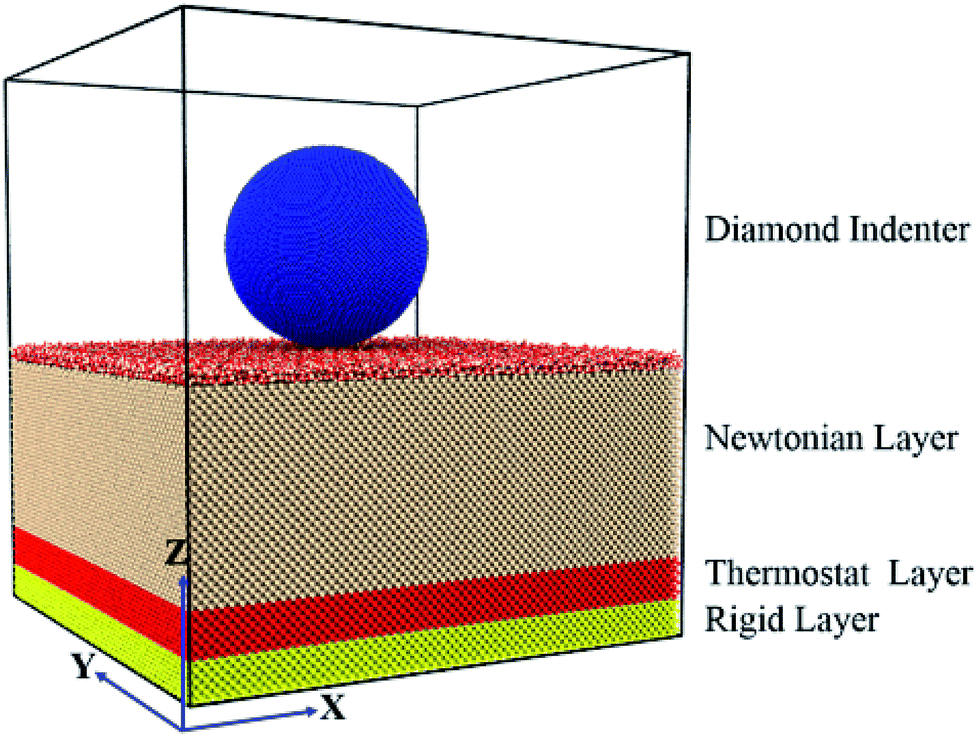 | ||
| Fig. 1 Schematic of the MD simulation for nanoindentation on the Si (001) surface covered with an amorphous SiO2 film. | ||
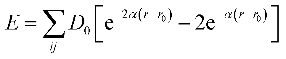
In order to deal with a model large enough to describe the Si–O system, we use the interatomic 3-body Tersoff potential21 designed for Si, O mixed system (Si–Si, Si–O, O–O within silicon substrate, SiO2 amorphous film and the interface between the two) developed by Munetoh et al.22 based on ab initio calculations, which is widely adopted to study the interactions of SiO2 and Si–O system.23,24 The widely used Morse potential25 is employed to depict the interactions between the Si atoms and C atoms of the diamond indenter with potential energy function expressed as
 | (1) |
Before loading, the system is relaxed in the NVT ensemble with the Nose–Hoover thermostat for 90 ps to minimize the energy. For following loading and unloading, the simulations are implemented in the NVE ensemble with the Langevin thermostat to maintain the temperature of thermostat layer at 300 K. The equations of motion are integrated with velocity-Verlet algorithm with a time step of 0.5 fs. The indentation speed of the indenter along Z direction is 25 m s−1 for both loading and unloading under displacement control and the maximum depth is set to 3.2 nm.
3 Results and discussions
3.1 Mechanical properties
To study the mechanical properties and deformation behaviors, a series of nanoindentation simulations is conducted on monocrystalline silicon substrate covered with an amorphous SiO2 film with different thickness of 0.4 nm, 0.6 nm, 0.8 nm, 1.0 nm, 1.4 nm and 2.0 nm, respectively. Based on the indentation data of designed samples typical nanoindentation curves of force–indentation depth are obtained, as shown in Fig. 2. Compared with the loading curves of force–indentation depth curves, all the unloading curves present significantly hysteresis indicating that massive plastic deformation occurs during nanoindentation process. Additional, it is interesting to note that all loading segments exhibit similar characteristic with the “serrate” style, a typical characteristics caused by local inhomogeneous plastic deformation, which has been considered as a signature of instabilities triggered by the bursts of plasticity under displacement control.26 This phenomena is also found in nanoindentation tests of metallic film27,28 and bulk amorphous metallic glasses.29 The inset is a detailed view of the partial loading curves, it shows that the “serrate” style for 0.6 nm and 0.8 nm is slightly stronger than those of other films.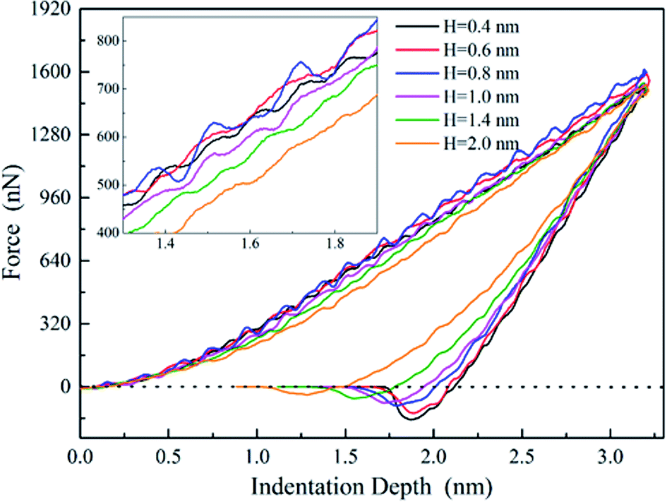 | ||
| Fig. 2 Force–indentation depth curve under different SiO2 film thickness (H). | ||
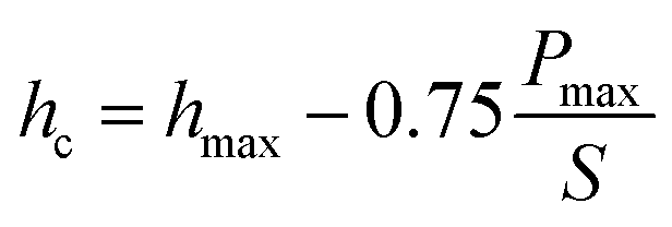
According to the methodology of Oliver and Pharr,12 nanoindentation mechanical properties (indentation modulus and hardness) of the designed samples mentioned above are derived from one complete cycle of loading and unloading. The mechanical property curves are calculated by fitting the unloading curve to the nonlinear relation
| P = B(h − hf)m | (2) |
 | (3) |
 | (4) |
 | (5) |
 | (6) |
The effective indentation modulus takes into the fact account that elastic displacement takes place in both tested samples and indenter. E, Ei, υ and υi denote the indentation modulus and Poisson's ratio of the tested samples and indenter, respectively. After massive indentation experiments, the mechanical properties of tested samples at various maximum indentation depth are calculated from eqn (2)–(6) mentioned above, and the indentation modulus and hardness as a functions of indentation depth are obtained and plotted in Fig. 3 and 4. It shows that for all the films the indentation modulus and hardness of tested samples increase with the growing indentation depth due to strongly substrate effect, for instance ranging from 79.9 GPa, 8.0 GPa at the depth of 0.8 nm up to 131.3 GPa, 21.2 GPa at the depth of 3.2 nm for 2.0 nm film sample, respectively. It also exhibits that the indentation modulus decreases dramatically with the increase of the film thickness at the same indentation depth, e.g. descent from 136.6 GPa for 0.4 nm film to 73.9 GPa for 2.0 nm film at the depth of 0.8 nm, and this variation trend is in good agreement with composite experiments reported by Xu,30 while variation of hardness is rather complex at the same depth. At shallow indentation depth of 0.8 nm and 1.6 nm, the hardness except for those of 0.6 nm and 0.8 nm films decreases slightly with the growing film thickness because of less substrate influence. Interestingly, for 0.6 nm and 0.8 nm film, the hardness is apparently larger than those of other films at the same depth of 1.6 nm because of the presence of intense inhomogeneous plastic deformation, exhibiting “serrate” style, which has the distinct influence on the calculated hardness and enhances the hardness. Contrarily, the hardness increases marginally with the increase of film thickness at the depth of 3.2 nm, because at such a large indentation depth the Si–O chemical bonds within thinner SiO2 films begin to bread down, which leads to the descent of hardness.
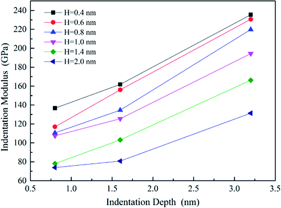 | ||
| Fig. 3 Indentation modulus vs. indentation depth under various film thickness (H). | ||
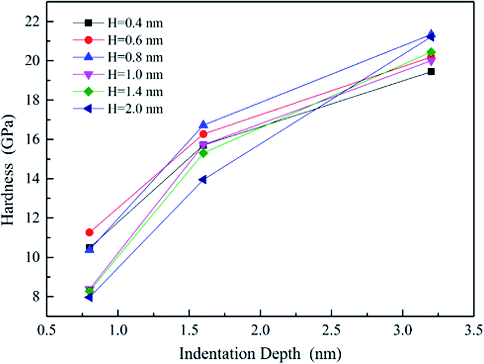 | ||
| Fig. 4 Hardness vs. indentation depth under various film thickness (H). | ||
It is worth noting that the SiO2 film with different thickness just only undergoes densification and thinning without rupture during whole nanoindentation process at various maximum indentation depth, even at the maximum depth of 3.2 nm, detailed discussions of SiO2 deformation are given in the next section.
3.2 Deformation behaviors of SiO2 film
The SiO2 film with amorphous structure of short-range order has continuous random network structure consisting of numerous SiO4 tetrahedra. In order to probe the deformation behaviors of the SiO2 film, the specific features of SiO2 film occurring underneath the diamond sphere are studied by nearest-neighbor radial distribution function (RDF) and bond angle distribution function (ADF). As shown in Fig. 5, taking indentation data at maximum depth (3.2 nm) as an example, the three peaks in initial SiO2 film (before loading) reflect Si–O, O–O and Si–Si separations at the average distance of 0.163 nm, 0.269 nm and 0.315 nm, respectively, which are in accordance well with experiment results.31 After loading (indentation depth reaches to its maximum value, but before unloading) the Si–O peak shifts right slightly. Meanwhile, its height decreases noticeably but the width increases on the contrary. The results imply an increase in the Si–O distance, and partial reverse changes take place after completely unloading. The positions of O–O, Si–Si peak remain as those in initial SiO2 film under both conditions of after loading and after unloading. Noted that two extra small peaks appear at the distance of 0.20 nm, 0.24 nm between Si–O and O–O peak under all the conditions except for 0.4 nm film after loading, and the position of the first small peak remains unchanged and its height decreases, while the second one disappears because of elastic recovery after completely unloading.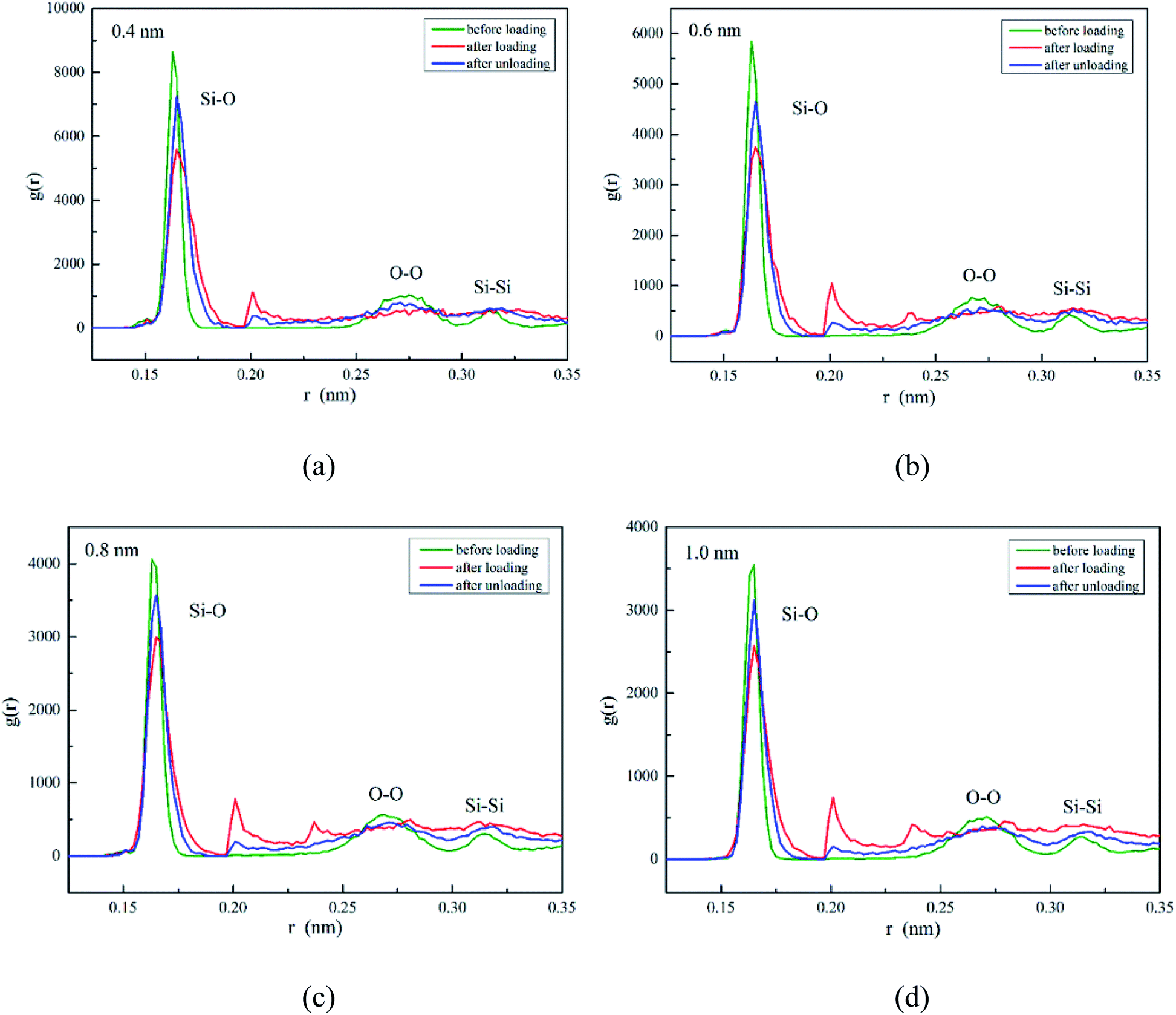 | ||
| Fig. 5 RDF for three states SiO2 film under different film thickness (H): (a) H = 0.4 nm, (b) H = 0.6 nm, (c) H = 0.8 nm, (d) H = 1.0 nm. | ||
In detail, the appearance of the two extra small peaks at about 0.20 nm, 0.24 nm is due to the decrease of partial O–O, Si–Si atom distance, respectively, which should be induced by the rotation and deformation of numerous SiO4 tetrahedra during loading. For instance (in Fig. 6), the distance of oxygen atoms 1–2, 2–3, 1–3 are 0.258 nm, 0.284 nm and 0.256 nm in initial SiO2 film, then they change to 0.200 nm, 0.228 nm and 0.320 nm after loading, finally they recover to 0.248 nm, 0.259 nm and 0.278 nm after completely unloading, respectively. This data indicates that the initial regular SiO4 tetrahedron becomes flattening along indentation direction (Z) as the indenter presses into SiO2 film, which recovers partially after completely unloading. However, the second small peak is absent in RDF of Fig. 5(a) because the thickness of 0.4 nm film decreases to the minimum compared with those of thicker films at the maximum depth and some Si–O covalent bonds break down during loading, resulting in the larger distance of Si–Si atoms.
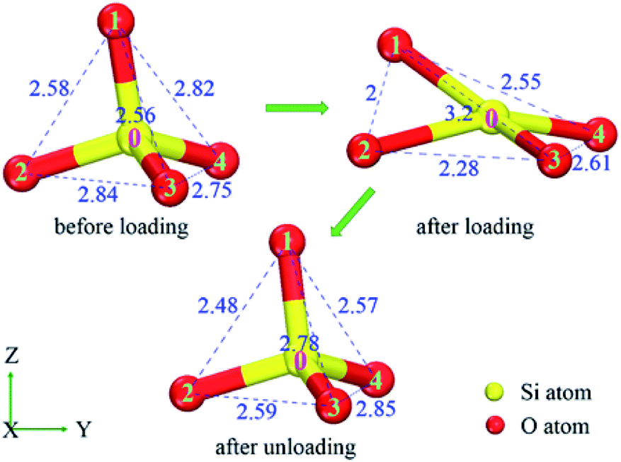 | ||
| Fig. 6 Change of atomic configurations for O–O distance (Å). | ||
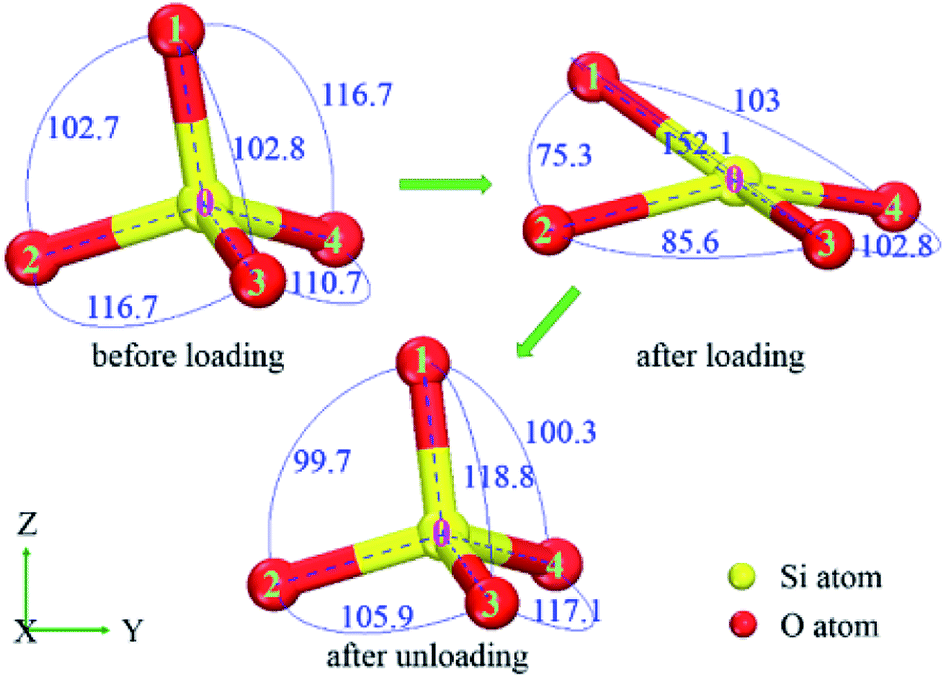
The ADF of O–Si–O for amorphous SiO2 film at different states (before loading, after loading, after unloading) is shown in Fig. 7. For all these simulations, the maximum distribution is at the ideal tetrahedral angel of 109.5° with a relatively narrow width initially. After loading, the width of the peak increases and the height decreases dramatically. Meanwhile, an extra peak appears at the position of about 73° during loading. Finally after unloading, partial reverse changes occur to the main peak and the small peak decreases in the height. The presence of the small peak indicates the decreasing of O–Si–O bond angle resulting from the rotation and deformation of numerous SiO4 tetrahedra. For instance (in Fig. 8), the O–Si–O bond angle of 1-0-2, 2-0-3 and 1-0-3 are 102.7°, 116.7° and 102.8° before loading, later they change to 75.3°, 85.6° and 152.1° after loading, finally they recover to 99.7°, 105.9° and 118.8° after totally unloading, respectively.
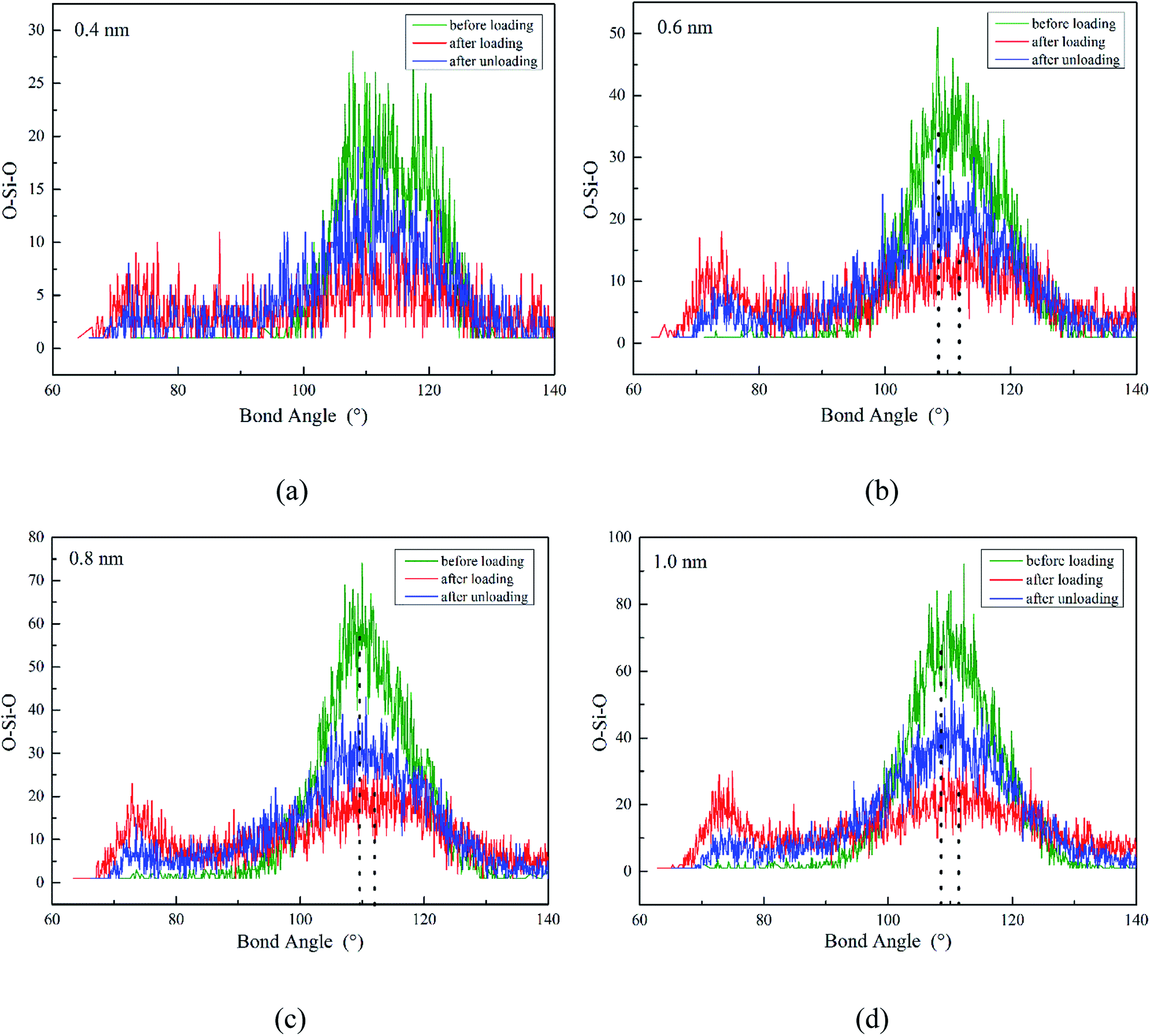 | ||
| Fig. 7 ADF of O–Si–O for three states SiO2 film under different film thickness (H): (a) H = 0.4 nm, (b) H = 0.6 nm, (c) H = 0.8 nm, (d) H = 1.0 nm. | ||
 | ||
| Fig. 8 Change of atomic configurations for O–Si–O angle (°). | ||
Based on the results of RDF and ADF for SiO2 film, a sequence of atomic configurations illustrates the deformation evolution of amorphous SiO2 just underneath the indenter, as shown in Fig. 9. It shows that the thickness of all these films decrease remarkably as indentation depth ranges from 0.0 nm to 0.8 nm, and then decrease slowly until the depth reaches to its maximum value, and finally the thickness of the deformed films increases gradually during unloading but not up to its original film thickness as the sphere indenter rises, which means that densification and thinning along indentation direction and extension in the deformed area take place. Especially for 0.4 nm film, the SiO2 film becomes the thinnest even reaching to a single atomic layer when the indentation depth is maximum at 3.2 nm.
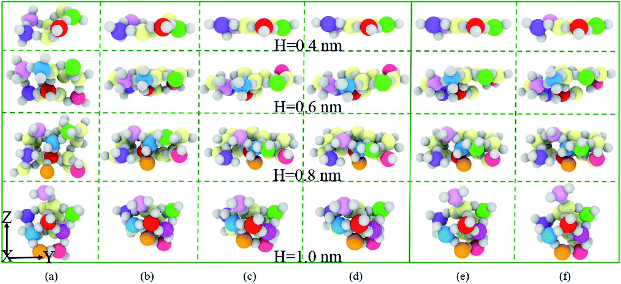 | ||
| Fig. 9 Partial cross-section snapshots of SiO2 deformation evolution under different film thickness (H): the indention depth of (a)–(d) during loading are 0.0 nm, 0.8 nm, 1.8 nm 3.2 nm. Those of (e) and (f) are 2.3 nm, 1.5 nm during unloading, respectively. The gray atoms present oxygen atoms, the others present silicon atoms, and the colored silicon atoms except yellow in the row trace the deformation by the same color. | ||
In order to carefully analyze the effect of film thickness on densification and extension of the SiO2 in Fig. 9, we propose the percentage of SiO2 densification ((film thicknessdepth=0.0 nm − film thicknessdepth=0.8 nm)/film thicknessdepth=0.0 nm) along indentation direction and extension ((widthdepth=0.8 nm − widthdepth=0.0 nm)/widthdepth=0.0 nm) in the vertical direction. As shown in Fig. 10, the percentage of densification increases significantly, while the percentage of extension decreases slightly with the increase of the film thickness. The evidences coupled with Fig. 9 imply that the thicker film has a potential to be further densification and extension and 0.4 nm film seems to reach its critical densification value (some Si–O bonds break down) at maximum indentation depth (3.2 nm) expecting to preferentially rupture during further loading, which give a reasonable explanation about 0.4 nm film with the smallest hardness at the depth of 3.2 nm.
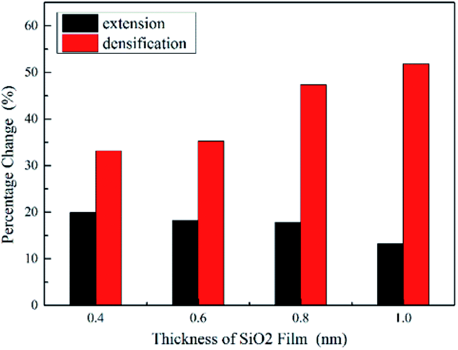 | ||
| Fig. 10 Percentage change of extension and densification vs. film thickness. | ||
3.3 Plastic deformation of silicon substrate
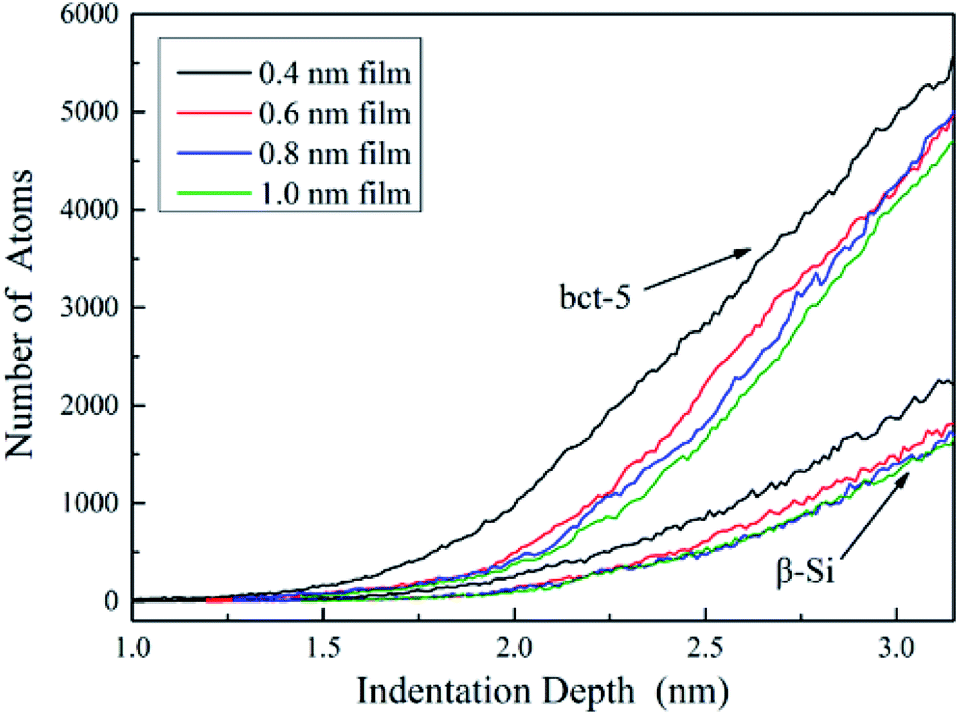
Silicon with 12 stable and metastable solid phases has been reported. Experiments employing diamond anvil cells to impose hydrostatic loading conditions and indentation tests have revealed that Si-I can be transformed to metallic Si-II at about 11.3 GPa, leading to ∼20% densification. At room temperature, the transition is not reversible and mixture of crystalline phase (Si-XII, Si-III) denote as mc-Si or amorphous silicon (a-Si) are formed in slow and rapid decompression, respectively.32–34 They concluded that phase transformation is the governing mechanism for inelastic deformation of silicon under contact loading.35–38 Thus the main work herein is to discuss silicon phase transformation under various film thickness.As the sphere indenter moves downwards, the SiO2 film firstly undergoes densification, which promotes deformation of the film as discussed in Section 3.2, and following the amorphous phase transformation of silicon substrate underneath the indenter occurs directly transformed from cd-Si owning to the distortion of silicon lattice39 according to the light load, which is in accordance well with massive nanoindentation experiments.35,40 As shown in Fig. 11, it exhibits a series of phase transformation evolution of silicon under different film thickness and that the amorphous phase transformation occurs within the surface and sub-surface of silicon substrate when the indentation depth is 0.8 nm. With growing indentation depth, the stress to silicon substrate increases, which leads to the phase transformation of silicon, underneath the layer of the newly generated amorphous silicon, from Si-I phase (cd-Si) to bct-5 (body-centered-tetragon) and β-Si (body-centered-tetragonal β-tin) phase.41 Therefore the silicon atom numbers of bct-5 and β-Si phase increase during loading, as shown in Fig. 12, which combined with Fig. 11 both validate the occurrence of the phase transformation. Additional, the results indicate that the phase transformation region of silicon substrate and the atom numbers of newly generated phases (amorphous, bct-5 and β-Si) decrease with increasing film thickness at the same indentation depth. However, the detailed analysis of silicon phase transformation during unloading are absent in this work, because the unloading rate in MD simulations is several orders of magnitude larger than nanoindentation experiments33,41,42 and the only amorphous silicon is found in deformed region. In this work, other phases of silicon are ignored because the corresponding atom numbers are too small or non-existent. It is concluded that we should protect the silicon substrate from been destroyed untimely and improve its life time by surface modification43 or by lubrication through controlling environment atmosphere9,44 in MEMS and electron devices, because a thinner SiO2 film endorses crystalline silicon phase transformation and growth in an oxygen environment.
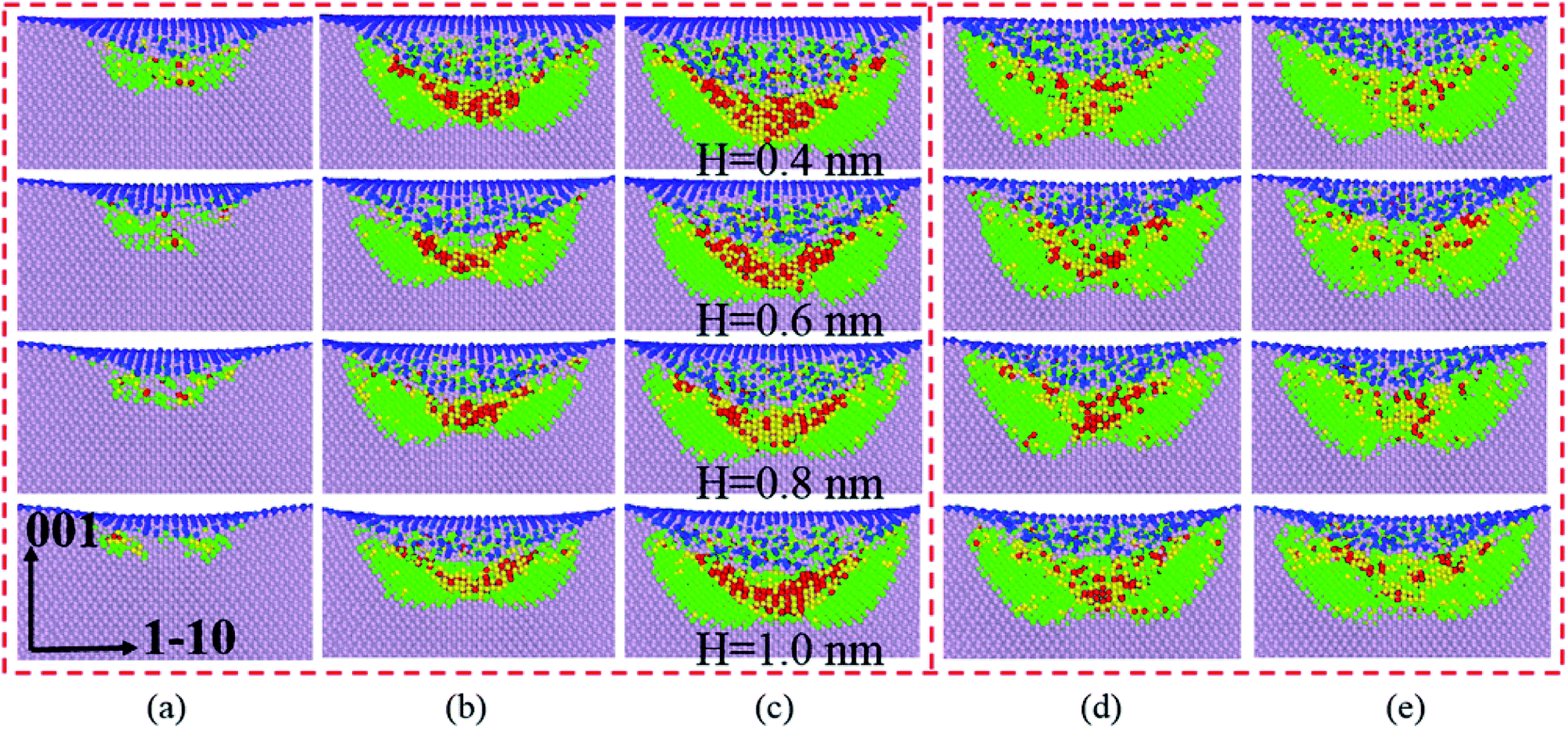 | ||
| Fig. 11 Cross-section snapshots of phase transformation evolution of silicon under various film thickness (H): the indention depth of (a)–(c) during loading are 0.8 nm, 1.8 nm 3.2 nm. Those of (d) and (e) are 2.3 nm, 1.5 nm during unloading, respectively. Atoms are colored according the coordinate number. The pink, green, yellow, blue and red ones are Si-I, bct-5, β-Si, surface atoms and other phase atoms, respectively. | ||
 | ||
| Fig. 12 Number of phase transformation atoms vs. indentation depth under various film thickness. | ||
3.4 Interface strength of SiO2/Si and stress distribution
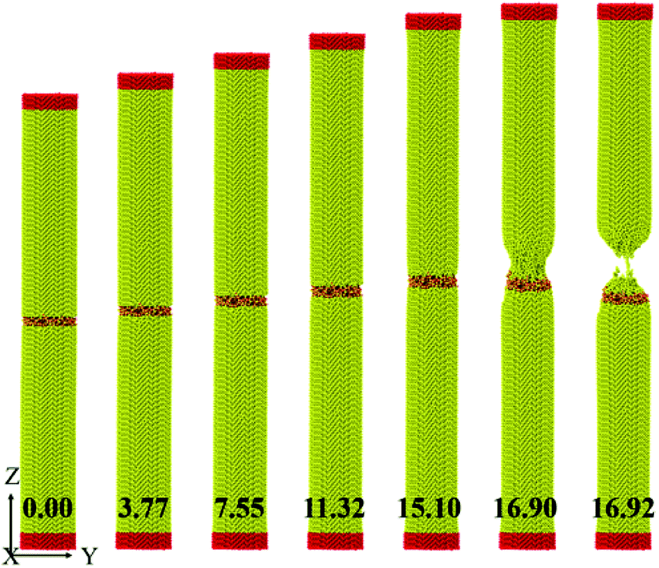
In order to investigate the interface strength between amorphous SiO2 film and silicon substrate, MD simulation of uniaxial tension is carried out. As shown in Fig. 13, the presented cylindrical model consists of monocrystalline silicon at the both ends and an amorphous SiO2 film with a thickness of 10 nm sandwiched between the silicon workpieces. The silicon workpiece for the upper part above the SiO2 film contains 34082 atoms with a size of 3.0 nm × 24.5 nm for radius and length, respectively. The silicon workpiece for the bottom part has the same parameters as upper workpiece. Therefore, the total length of the sandwiched structure is 50.0 nm with a radius of 3.0 nm. The crystal orientation of the silicon workpieces along the X, Y and Z are [100], [010] and [001], respectively, which as well as the potential employed to depict interactions of Si–O system are consistent with our nanoindentation tests. Details of simulation procedure of uniaxial tension are similar to Han's methods in ref. 45 The sandwiched structure is divided into deformation layer, fixed layer and loading layer. The fixed layer and loading layer are defined as rigid with the same parameters. Before loading in tension, we equilibrate the system for 90 ps as mentioned in Section 2. Thereafter, the uniaxial tension is performed by displacing the atoms in loading layer at a constant strain rate of 2.5 × 10⁷, while the atoms in fixed layer are frozen. The system maintains constant temperature of 300 K by NVT ensemble during tension process.
 | ||
| Fig. 13 Tensile deformation of Si/SiO2/Si sandwiched structure under different strain (ε: %). Except the fixed and loading red atoms at the both ends, other red and yellow atoms represent oxygen atoms and silicon atoms, respectively. | ||
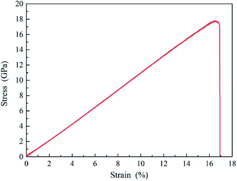
The displacement of upper part silicon is recorded and the typically stress–strain curve of uniaxial tension is derived, as shown in Fig. 14. It illustrates a linear elastic deformation until abrupt failure with the values of fracture stress and strain as 17.7 GPa and 16.9%, respectively, which are close to the Kang' simulations (about 13.3 GPa and 16.2%)46 and Tang's experiments results.47 Furthermore, the slope of the stress–strain curve during the linear elastic portion gives the Young's modulus (109.4 GPa), which is in good accordance with that of our nanoindentation test (110.6 GPa). Fig. 13 presents the deformation of uniaxial tension at different strain for the sandwich sample. It is observed that the sample is elongated uniformly at an average strain rate of 2.5 × 10⁷ in a large strain range from 0.00 to 15.10, as the strain increases to a certain value, the amorphous phase transformation of silicon in the outer layer of sample is observed and spreads toward the center in the neck region until the sample finally fractures. Beyond this region, the sample keeps ordered structure and has no significant change. Fortunately, because the fracture site is determined by the weakest spot, the fracture site in our uniaxial tension is within silicon workpiece rather than interfaces between SiO2 film and silicon, which directly certifies that the interface does not affect tension deformation behavior of silicon.
 | ||
| Fig. 14 Stress–strain curve of uniaxial tension for the sandwich sample. | ||
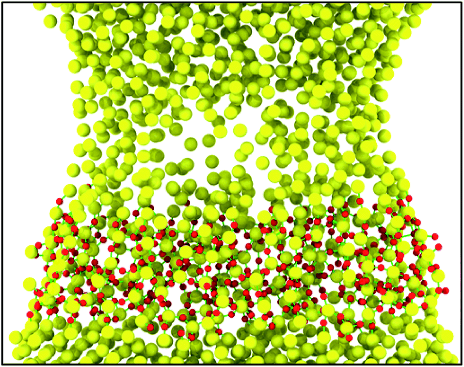
Fig. 15 presents the detailed interfacial structure of SiO2/Si at the strain of 16.90, showing that two segments of sandwich sample (amorphous SiO2 film and silicon) are densely connected by many chemical bonds and the bond energy of Si–O (542 kJ mol−1)48 is higher than that of Si–Si (222 kJ mol−1),49 which reasonably explains the reason why the sample fracture site is within silicon rather than SiO2/Si interfaces.
 | ||
| Fig. 15 Cross-section snapshot of SiO2/Si interface at the strain of 16.90 (%). The red and yellow colors represent oxygen atoms and silicon atoms, respectively. The green sticks present Si–O chemical bonds. | ||
Von Mises stress distribution of bilayer system at different indentation depth are carefully analyzed, finding that the stress increases with the growing indentation depth and local stress concentration appears within amorphous SiO2 film. Taking stress distribution of 2.0 nm film sample for instance in Fig. 16, the average stress of SiO2 film underneath sphere indenter is significant higher than that of surrounding silicon substrate. Such sharply changed shear stress (SCSS) is also happened to Yang's research,50,51 they presented that the interface SCSS increases with the increasing indentation depth. However, in our nanoindentation tests both the value and the increasing rate of SCSS are much less than that of Yang's results, which probably results from the different simulation size between MD simulations and finite element analysis.
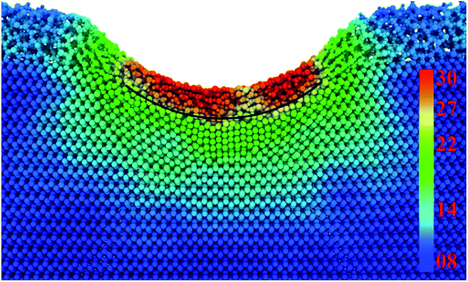 | ||
| Fig. 16 Cross-section of von Mises stress at the indentation depth of 3.2 nm for 2.0 nm film sample (GPa). | ||
4 Conclusions
In this paper, we have investigated the mechanical properties and deformation behaviors of surface modified silicon during chemical mechanical polishing (CMP) process based on the molecular dynamic simulation, the conclusions can be drawn as following:(1) Indentation mechanical properties can be determined by Olive and Pharr's methodology, finding that both the indentation modulus and hardness increase significantly with the growing indentation depth owning to the strongly silicon substrate effect. At the same indentation depth, the indentation modulus decreases shapely with the increase of film thickness because of less substrate influence, while the hardness agrees well with the trend of modulus at shallow depth but mismatches at larger indentation depth.
(2) By carefully discussions of the RDF and ADF for SiO2 film, it shows that the rotation and deformation of massive SiO4 tetrahedra promote the densification and thinning along the indentation direction and extension in the deformed area, which results in the rupture of the thinner film (than 0.4 nm) preferentially.
(3) The SiO2 film plays an important role in resisting silicon phase transformation. The thinner the SiO2 film is, the earlier the silicon phase transformation takes place. The bct-5 and β-Si silicon, the primarily concerned phase in the nanoindentation tests, grow massively below the indenter during loading. Therefore the numbers of phase transformation atoms increase with the decrease of SiO2 film thickness at the same indentation depth.
(4) The thicker film turns out to be a better than a thinner one, as one could obtain higher material removal rate and less defects within silicon substrate in CMP process.
(5) Interface strength of SiO2/Si is carefully analyzed by uniaxial tension simulation, indicating that interfaces have little effect on tension deformation behavior of silicon because of densely connected chemical bonds between amorphous SiO2 film and silicon.
Conflicts of interest
There are no conflicts of interest to declare.Acknowledgements
The authors wish to thank Zhi Chen for his contribution to bond angle distribution function. This study was supported by the National Natural Science Foundation of China [grant numbers 51375364, 51475359, 51605139, 51505479], the Natural Science Foundation of Shaanxi Province [2014JM6219] and Natural Science Foundation of Jiangsu Province of China (BK20160867, BK20150184).References
- X. Wang, S. H. Kim, C. Chen, L. Chen, H. He and L. Qian, ACS Appl. Mater. Interfaces, 2015, 7, 14785–14792 CAS.
- Y. Lee, Y.-J. Seo and H. Jeong, Electron. Mater. Lett., 2012, 8, 523–528 CrossRef CAS.
- G. J. Pietsch, Y. J. Chabal and G. S. Higashi, Surf. Sci., 1995, 331, 395–401 CrossRef.
- J. Xu, J. B. Luo, L. L. Wang and X. C. Lu, Tribol. Int., 2007, 40, 285–289 CrossRef CAS.
- W.-E. Fu, C.-C. A. Chen, Y.-D. Lin, Y.-Q. Chang and Y.-H. Huang, Thin Solid Films, 2011, 519, 4874–4879 CrossRef CAS.
- E. Estragnat, G. Tang, H. Liang, S. Jahanmir, P. Pei and J. M. Martin, J. Electron. Mater., 2004, 33, 334–339 CrossRef CAS.
- F. Katsuki and J. Watanabe, in Fundamentals of Nanoindentation and Nanotribology III, ed. K. J. Wahl, N. Huber, A. B. Mann, D. F. Bahr and Y. T. Cheng, 2005, vol. 841, pp. 253–258 Search PubMed.
- G. J. Pietsch, G. S. Higashi and Y. J. Chabal, Appl. Phys. Lett., 1994, 64, 3115–3117 CrossRef CAS.
- J. Yu, S. H. Kim, B. Yu, L. Qian and Z. Zhou, ACS Appl. Mater. Interfaces, 2012, 4, 1585–1593 CAS.
- M. Forsberg, Microelectron. Eng., 2005, 77, 319–326 CrossRef CAS.
- W. Maw, F. Stevens, S. C. Langford and J. T. Dickinson, J. Appl. Phys., 2002, 92, 5103–5109 CrossRef CAS.
- W. C. Oliver and G. M. Pharr, J. Mater. Res., 2004, 19, 3–20 CrossRef CAS.
- H. Sitinamaluwa, J. Nerkar, M. Wang, S. Zhang and C. Yan, RSC Adv., 2017, 7, 13487–13497 RSC.
- W. C. Oliver and G. M. Pharr, J. Mater. Res., 1992, 7, 1564–1583 CrossRef CAS.
- Z. S. Ma, Y. C. Zhou, S. G. Long and C. Lu, Int. J. Plast., 2012, 34, 1–11 CrossRef CAS.
- S. A. S. Asif, K. J. Wahl and R. J. Colton, J. Mater. Res., 2000, 15, 546–553 CrossRef CAS.
- J. P. Chu, J. S. C. Jang, J. C. Huang, H. S. Chou, Y. Yang, J. C. Ye, Y. C. Wang, J. W. Lee, F. X. Liu, P. K. Liaw, Y. C. Chen, C. M. Lee, C. L. Li and C. Rullyani, Thin Solid Films, 2012, 520, 5097–5122 CrossRef CAS.
- J. F. Luo and D. A. Dornfeld, IEEE Trans. Semicond. Manuf., 2001, 14, 112–133 CrossRef.
- S. Plimpton, J. Comput. Phys., 1995, 117, 1–19 CrossRef CAS.
- S. C. Chowdhury, B. Z. Haque and J. W. Gillespie Jr, J. Mater. Sci., 2016, 51, 10139–10159 CrossRef CAS.
- J. Tersoff, Phys. Rev. B: Condens. Matter Mater. Phys., 1989, 39, 5566–5568 CrossRef.
- S. Munetoh, T. Motooka, K. Moriguchi and A. Shintani, Comput. Mater. Sci., 2007, 39, 334–339 CrossRef CAS.
- S. Zhao and J. Xue, Carbon, 2015, 93, 169–179 CrossRef CAS.
- J. Chen, G. Zhang and B. W. Li, J. Appl. Phys., 2012, 112, 7 Search PubMed.
- J. Shi, J. Chen, X. Wei, L. Fang, K. Sun, J. Sun and J. Han, RSC Adv., 2017, 7, 30929–30940 RSC.
- K. Srikanth and G. Ananthakrishna, Phys. Rev. B: Condens. Matter Mater. Phys., 2017, 95 Search PubMed.
- A. Gouldstone, H. J. Koh, K. Y. Zeng, A. E. Giannakopoulos and S. Suresh, Acta Mater., 2000, 48, 2277–2295 CrossRef CAS.
- P. Peng, G. Liao, T. Shi, Z. Tang and Y. Gao, Appl. Surf. Sci., 2010, 256, 6284–6290 CrossRef CAS.
- Y. I. Golovin, V. I. Ivolgin, V. A. Khonik, K. Kitagawa and A. I. Tyurin, Scr. Mater., 2001, 45, 947–952 CrossRef CAS.
- K. W. Xu, G. L. Hou, B. C. Hendrix, J. W. He, Y. Sun, S. Zheng, A. Bloyce and T. Bell, J. Mater. Res., 1998, 13, 3519–3526 CrossRef CAS.
- W. Jin, R. K. Kalia, P. Vashishta and J. P. Rino, Phys. Rev. Lett., 1993, 71, 3146–3149 CrossRef CAS PubMed.
- M. Budnitzki and M. Kuna, J. Mech. Phys. Solids, 2016, 95, 64–91 CrossRef CAS.
- S. Goel, X. C. Luo, A. Agrawal and R. L. Reuben, International Journal of Machine Tools and Manufacture, 2015, 88, 131–164 CrossRef.
- Y.-H. Lin, T.-C. Chen, P.-F. Yang, S.-R. Jian and Y.-S. Lai, Appl. Surf. Sci., 2007, 254, 1415–1422 CrossRef CAS.
- I. Zarudi and L. C. Zhang, Tribol. Int., 1999, 32, 701–712 CrossRef CAS.
- S. Goel, A. Kovalchenko, A. Stukowski and G. Cross, Acta Mater., 2016, 105, 464–478 CrossRef CAS.
- S. Goel, N. H. Faisal, X. Luo, J. Yan and A. Agrawal, J. Phys. D: Appl. Phys., 2014, 47 Search PubMed.
- J. Sun, C. Li, H. Jing, A. Ma and L. Fang, Sci. Rep., 2017, 7 Search PubMed.
- Y. Q. Wu, X. Y. Yang and Y. B. Xu, Acta Mater., 1999, 47, 2431–2436 CrossRef CAS.
- I. Zarudi, W. C. D. Cheong, J. Zou and L. C. Zhang, Nanotechnology, 2004, 15, 104–107 CrossRef CAS.
- J. Sun, A. Ma, J. Jiang, J. Han and Y. Han, J. Appl. Phys., 2016, 119, 095904–095909 CrossRef.
- J. Han, S. Xu, J. Sun, L. Fang and H. Zhu, RSC Adv., 2017, 7, 1357–1362 RSC.
- B. Bhushan and V. N. Koinkar, Appl. Phys. Lett., 1994, 64, 1653–1655 CrossRef CAS.
- D. B. Asay, M. T. Dugger, J. A. Ohlhausen and S. H. Kim, Langmuir, 2008, 24, 155–159 CrossRef CAS PubMed.
- J. Han, L. Fang, J. Sun, Y. Han and K. Sun, J. Appl. Phys., 2012, 112, 114314 CrossRef PubMed.
- K. W. Kang and W. Cai, Int. J. Plast., 2010, 26, 1387–1401 CrossRef CAS.
- D. M. Tang, C. L. Ren, M. S. Wang, X. Wei, N. Kawamoto, C. Liu, Y. Bando, M. Mitome, N. Fukata and D. Golberg, Nano Lett., 2012, 12, 1898–1904 CrossRef CAS PubMed.
- X. D. Wang, J. Guo, C. Chen, L. Chen and L. M. Qian, J. Appl. Phys., 2016, 119, 044304 CrossRef.
- S. Yajima, Y. Hasegawa, J. Hayashi and M. Iimura, J. Mater. Sci., 1978, 13, 2569–2576 CAS.
- Y. Yang, N. Liao, M. Zhang and F. Li, J. Alloys Compd., 2017, 710, 468–471 CrossRef CAS.
- Y. Yang, N. Liao, M. Zhang and F. Li, J. Eur. Ceram. Soc., 2017, 37, 3891–3897 CrossRef CAS.
| This journal is © The Royal Society of Chemistry 2018 |