
 Open Access Article
 This Open Access Article is licensed under a Creative Commons Attribution-Non Commercial 3.0 Unported Licence
Physical process-aided fabrication of periodic Au–M (M = Ag, Cu, Ag–Cu) alloyed nanoparticle arrays with tunable localized surface plasmon resonance and diffraction peaks†
Honghua Zhang a,
Chu Wanga,
Huilin Lib,
Longfa Jiangc,
Dandan Mena,
Jun Wanga and
Junhuai Xiang*a
a,
Chu Wanga,
Huilin Lib,
Longfa Jiangc,
Dandan Mena,
Jun Wanga and
Junhuai Xiang*a
aJiangxi Key Laboratory of Surface Engineering, Jiangxi Science and Technology Normal University, Nanchang 330013, P. R. China
bKey Lab of Materials Physics, Anhui Key Lab of Nanomaterials and Nanotechnology, Institute of Solid State Physics, Chinese Academy of Sciences, Hefei 230031, P. R. China
cComprehensive Technology Center, Jiangxi Entry-Exit Inspection and Quarantine Bureau, Nanchang 330031, P. R. China. E-mail: xiangjunhuai@163.com
First published on 1st March 2018
Abstract
Periodic alloyed (Au–Ag, Au–Cu, Au–Ag–Cu) nanoparticle (NP) arrays with uniform size, controllable composition and center-to-center spacing were fabricated by a novel and facile strategy based on physical vapor deposition on a monolayer colloidal crystal template and further heat treatment. The composition and center-to-center spacing were manipulated by adjusting the sputtering target in the deposition process and the size of colloidal spheres of the template, respectively. The shadow effect and a dewetting model were employed to analyze the whole process of evolution from a metallic thin film to spherical nanoparticles with uniform size. The localized surface plasmon resonance (LSPR) and diffraction peaks of these alloyed arrays were systematically measured. The dielectric constant has an important influence on LSPR peaks and diffraction peaks. Both the LSPR and diffraction peaks of Au–Ag alloyed NPs arrays exhibit a blue shift due to their lower dielectric constant than that of pure Au NPs. However, compared with Au, Cu possesses a higher dielectric constant, leading to a red shift of the LSPR and diffraction peaks of Au–Cu alloyed NPs arrays. With the increase of NP size, the diffraction peaks of both binary alloyed NPs exhibit a slight red shift. Moreover, the LSPR absorption peaks were more sensitive to the composition of the NPs than the diffraction peaks. This work would open up a novel strategy in the production of alloyed NP arrays with tunable LSPR peaks and diffraction peaks, which would be very helpful to improve their practical applications in various fields.
1. Introduction
Noble metal, such as Au, Ag and Cu, alloyed nanoparticles (NPs) have better comprehensive physical, chemical, and mechanical performance than their pure analogues due to synergistic effects of their constituent components.1–3 In particular, localized surface plasmon resonance (LSPR) can readily be tuned by producing alloyed NPs, which expands their applications in many fields,4–9 including bioimaging, catalytic, therapy, and surface-enhanced Raman scattering (SERS). The LSPR properties of the alloyed NPs are closely related to content of each ingredient, size, and morphologies.10,11 Therefore, the fabrication of the noble metal alloyed NPs with different contents, various morphologies and sizes have recently attracted increasing attention.For now, noble metal alloyed NPs are fabricated mainly using chemical reduction method in solution (also called wet-chemical syntheses).12–15 For example, Swihart's group synthesized Au–Ag alloyed NPs by mixing metal precursors and surfactants in organic solvent, and further heating together.16 The LSPR peak of the Au–Ag alloyed NPs in their report could be tuned by varying the precursor or the added surfactants composition. Although this method is feasible, it is unable to precisely control the shape and size.17 Moreover, the surface of NPs fabricated by this method contains surfactant inevitably, which would seriously hinder further functionalization and cause interference to the test results.18 Additionally, thermal plasma assisted gas phase condensation method has also been used to fabricate alloyed NPs. Nevertheless, this method is limited to special applications due to their high processing costs.3 Therefore, it becomes more important to offer a fabrication method of noble metal alloyed NPs with controllable microstructure, low cost and without surfactant.
Recently, Dong's group fabricated the CoPt NP-based nanoline and nanodot arrays by nanoimprinting the polymer blend of CoPt-containing metallopolymer and polystyrene followed by pyrolysis.14 Wang and co-workers present a novel method based on combination of chemical and physical method to synthesize Au–Cu and Au–Ag–Cu alloyed NPs by starting from Au@Cu2O core–shell NPs prepared by chemical reduction, then annealing in a H2 atmosphere.19,20 The surface of the nanoparticle prepared by this method contains no surfactant. However, the preparation process of Au@Cu2O core–shell NPs is complex and uncontrolled. Li and co-workers fabricated Au21,22 and Cu NPs23 arrays using physical methods, which typically involved depositing a layer of Au or Cu film on two-dimension (2D) polystyrene (PS) nanospheres array template, and then annealing. The original PS template was burned out and the deposited Au coating on it was melted and collapsed and occupied the place of original PS sphere, then formed Au nanospheres during the annealing process. This method offered precise control over the size and uniformity of the NPs array without surfactant. If one can deposit a layer of pure Ag, pure Cu or Ag–Cu complex film on the above Au arrays, followed by annealing, a facile and highly efficient synthetic method of alloyed NPs might be developed without complex chemical reaction. Au, Ag and Cu NPs typically have LSPR peak around 530 (ref. 21), 400 (ref. 16) and 580 nm,24 respectively. Hence, the LSPR peak between 400 and 580 nm can be adjusted by producing Au–Ag, Au–Cu and Au–Ag–Cu alloyed NPs. In addition to LSPR peak, diffraction peaks also appear in these periodic arrays structure due to Bragg diffraction. Importantly, diffraction peaks are also sensitive to the composition of the alloyed NPs. The alloyed NPs array with tunable LSPR and diffraction peaks would open up new application in therapy, visual sensor, SERS active substrates and so on. Particularly, the ordered array structure is helpful to improve the repeatability and stability of their properties. However, there are few reports on the construction of 2D periodic binary or ternary alloy NPs arrays using dewetting film route.
In this work, a novel and facile method based on template method for the fabrication of several ordered binary and ternary metallic alloyed NPs arrays (i.e. Au–Ag, Au–Cu and Au–Ag–Cu) in large-scale with control of particle size, composition and periodicity was presented. The fabrication process involved two steps. Firstly, Au nanospheres array was prepared by using 2D PS nanospheres array as a starting template; secondly, the as-prepared 2D Au nanospheres array was served as the secondary template and providing substrate for an Ag or Cu layer, or binary Ag–Cu metallic film to deposit on, and followed by annealed at an H2 atmosphere. Compared with pure Au nanospheres array, both the LSPR and diffraction peak of Au–Ag alloyed NPs array blue shifted, but red shifted for Au–Cu alloyed NPs array. Additionally, the LSPR peak was more sensitive to the composition of NPs than the diffraction peaks.
2. Experimental
2.1 Materials
Monodispersed PS microsphere suspension (2.5 wt% in water) with diameter of 500 nm, 750 nm, and 1000 nm were purchased from Alfa Aesar Corporation. All the three kinds of high pure (99.99%, φ55 × 3 mm) targets of Au, Ag and Cu in sputtering process were bought from China Material Technology Co. Ltd. The quartz sheets were used as substrates for self-assembly of PS spheres offered by TRION Technology Corporation. The high-purity mixed gas (N2 (96%), H2 (4%)) was bought from Nanchang Guoteng Gas Factory Corporation. Acetone, ethanol, H2O2, NH3·H2O, H2SO4 with analytical grade were bought from China Material Technology Co. Ltd. Deionized water (18.2 MΩ cm) used in all experiments was obtained from ultrafiltration system.2.2 Fabrication of periodic alloyed NPs arrays
Firstly, the quartz sheets were ultrasonically washed with acetone, ethanol and deionized water for 40 min, respectively, followed by soaking in H2SO4/H2O2 (3![[thin space (1/6-em)]](https://www.rsc.org/images/entities/char_2009.gif) :1 in volume) for 8 h and ultrasonically washed for 40 min. Afterwards, the quartz sheets were washed in H2O/H2O2/NH3·H2O (3:1:1 in volume) and deionized water for 40 min, respectively. Lastly, the quartz sheets were irradiated in ultraviolet-ozone cleaning machine for 30 min. After the above-mentioned treatment, the quartz sheets with good surface hydrophilicity were obtained. Subsequently, PS microsphere suspensions were mixed evenly with the equal volume of ethanol/acetone (1:1 in volume) by the ultrasonic bath for 10 min. Monolayer PS microspheres arrays were fabricated on the substrate at interfaces of gas–liquid phase as reported by us previously,25 as shown in Fig. 1a. Then, the Au film was deposited on the prepared substrate surface by magnetron sputtering deposition technology (CRESSINGTON, Sputter Coater 108) at 35 mA for 80 s. After heating at 1000 °C for 2 h in a tube furnace, ordered near-spherical Au NPs array can be obtained on the substrate, as shown in Fig. 1b and c. In order to obtain alloyed NPs arrays, Ag film, Cu film and Ag–Cu complex film were deposited at 35 mA for 40 s, 40 s and 40 s (Ag: 20 s; Cu: 20 s) on the surface of the Au nanosphere arrays, respectively. By heating at 750 °C for 3 h in a tube furnace under a mixed gas N2 + H2 (4% H2 in volume) atmosphere, the binary Au–Ag, Au–Cu alloyed and ternary Au–Ag–Cu alloyed spherical ordered NPs array were obtained on the substrates, as shown in Fig. 1d and e.
:1 in volume) for 8 h and ultrasonically washed for 40 min. Afterwards, the quartz sheets were washed in H2O/H2O2/NH3·H2O (3:1:1 in volume) and deionized water for 40 min, respectively. Lastly, the quartz sheets were irradiated in ultraviolet-ozone cleaning machine for 30 min. After the above-mentioned treatment, the quartz sheets with good surface hydrophilicity were obtained. Subsequently, PS microsphere suspensions were mixed evenly with the equal volume of ethanol/acetone (1:1 in volume) by the ultrasonic bath for 10 min. Monolayer PS microspheres arrays were fabricated on the substrate at interfaces of gas–liquid phase as reported by us previously,25 as shown in Fig. 1a. Then, the Au film was deposited on the prepared substrate surface by magnetron sputtering deposition technology (CRESSINGTON, Sputter Coater 108) at 35 mA for 80 s. After heating at 1000 °C for 2 h in a tube furnace, ordered near-spherical Au NPs array can be obtained on the substrate, as shown in Fig. 1b and c. In order to obtain alloyed NPs arrays, Ag film, Cu film and Ag–Cu complex film were deposited at 35 mA for 40 s, 40 s and 40 s (Ag: 20 s; Cu: 20 s) on the surface of the Au nanosphere arrays, respectively. By heating at 750 °C for 3 h in a tube furnace under a mixed gas N2 + H2 (4% H2 in volume) atmosphere, the binary Au–Ag, Au–Cu alloyed and ternary Au–Ag–Cu alloyed spherical ordered NPs array were obtained on the substrates, as shown in Fig. 1d and e.
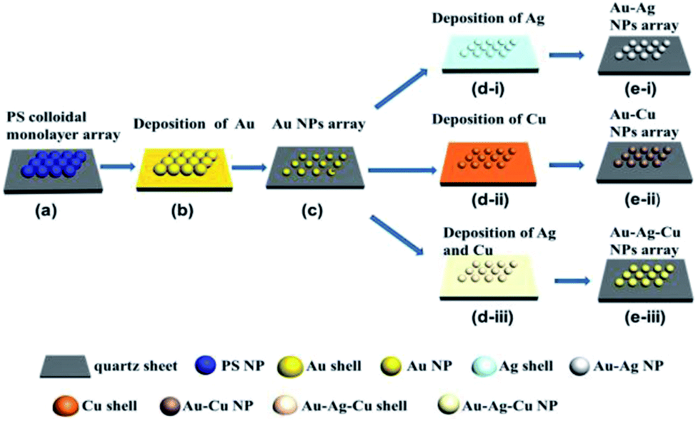 | ||
| Fig. 1 Fabrication route of periodic alloyed nanospheres arrays. (a) Monolayer colloidal crystal template was made on quartz sheet by self-assembling method. (b) After magnetron sputtering deposition, the Au thin film was deposited onto the surface of colloidal monolayer. (c) Periodic Au spherical NPs arrays were formed by annealing at 1000 °C for 2 h at air atmosphere. (d) Ag thin film (i), Cu thin film (ii) and Ag–Cu complex film (iii) were deposited on the surface of periodic Au spherical NPs arrays by magnetron sputtering deposition technology. (e) After annealing in reducing atmosphere (N2 (96%), H2 (4%), volume ratio) at 750 °C for 2 h, Au–Ag(I), Au–Cu(II) and Au–Ag–Cu(III) alloyed NPs ordered arrays were fabricated. | ||
2.3 Characterization
Morphologies and compositions of periodic arrays were characterized by field emission scanning electron microscope (FE-SEM, Zeiss sigma) equipped with energy disperse spectrum of X-ray analysis system (EDS, Oxford INCA). Microstructure of a single isolated Au–Ag–Cu alloyed NPs was characterized by transmission electron microscope (TEM, JEM-2010F, JEOL). In addition, the phase structures were analyzed by X-ray diffraction (XRD, Shimadzu XRD-6100 with Cu K-alpha radiation λ = 0.15419 nm). UV-Vis extinction spectra were obtained on an ultraviolet visible spectrometer (MAPADA UV-6100) with high wavelength resolution of 0.5 nm.3. Results and discussion
3.1 Morphology and structural characterization
SEM top-view images of the ordered alloyed NPs arrays including Au–Ag, Au–Cu and Au–Ag–Cu alloy are shown in Fig. 2a–c, respectively. The three kinds of alloyed NPs arrays exhibit hexagonal non-closed arrangement with the central distance between the two nearest-neighbouring structural units of 500 nm. It indicates that each structural unit has near-spherical shape with uniform size, and the average diameter of Au–Ag, Au–Cu and Au–Ag–Cu alloyed particle was 243, 196, 230 nm, respectively. The element mapping analysis of Au–Ag and Au–Cu confirmed that Au and Ag or Cu elements were uniformly distributed in the total NPs, respectively. For Au–Ag–Cu NPs array, it could be seen that Au, Ag and Cu elements were homogeneously distributed in the NPs (Fig. 2c). Element line-scanning distribution images of Au–Ag, Au–Cu and Au–Ag–Cu alloyed NPs arrays (Fig. S1–S3†) also exhibited the same varying tendency with the particle spatial distribution. All these results demonstrated that binary Au–Ag, Au–Cu and ternary alloyed Au–Ag–Cu NPs array was successfully prepared.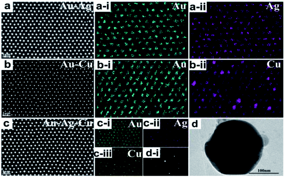 | ||
| Fig. 2 SEM plan-view images and corresponding EDS elemental distributing map of alloyed NPs arrays templated by colloidal monolayer with periodic length of 500 nm: Au–Ag (a), Au–Cu (b), Au–Ag–Cu (c) alloyed NPs arrays. (d) TEM image of a single isolate Au–Ag–Cu NP, (d–i) Electron diffraction pattern of the single isolate Au–Ag–Cu NP. | ||
Specially, a single isolate Au–Ag–Cu ternary alloyed NPs was further characterized by TEM, as shown in Fig. 2d. The shape of nanoparticle exhibits spherical crown shape, and it only has a little flat piece on the bottom. The reason is that during annealing process at 1000 °C, the nanoparticle maintains liquid state and has a certain contact area (facet contact) with the supporting substrate, and the original state was maintained during the subsequent cooling and solidification process. Fig. 2d-i shows bright and clear electronic diffraction spots of the single isolate Au–Ag–Cu NP. In addition, the Au–Ag NPs arrays with periodic length of 750 nm and the Au–Ag–Cu NPs arrays with periodic length of 1000 nm were prepared, as shown in Fig. S4 and S5.†
Crystal structures of the Au–Ag, Au–Cu and Au–Ag–Cu alloyed NPs array and bared quartz wafer were characterized by XRD, as shown in Fig. 3. In XRD pattern of Fig. 3, the four curves from bottom to top correspond to samples of bared quartz substrate, Au–Ag, Au–Cu and Au–Ag–Cu NPs array, respectively. Bared quartz substrate served as a reference sample has no obvious peak. However, the XRD pattern of Au–Ag, Au–Cu and Au–Ag–Cu NPs array exhibit obvious crystal diffraction peaks positioned at 38°, 45°, 64°, 78° in sequence, corresponding to particular lattice plane (111), (200), (220), (311) of alloyed metallic crystal particle, respectively. The XRD results demonstrate that the Au–Ag, Au–Cu and Au–Ag–Cu NPs are face-centered cubic structure and have good crystallinity with a strong (111) orientation.
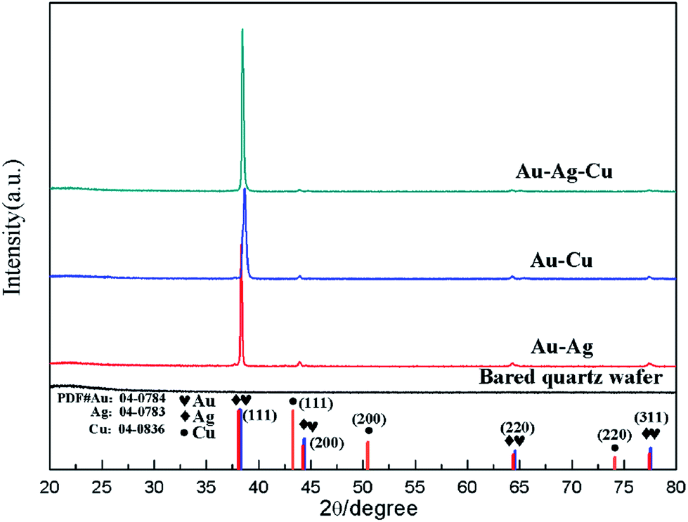 | ||
| Fig. 3 XRD pattern of obtained periodic alloyed NPs arrays by colloidal monolayer crystal with periodicity of 500 nm. | ||
3.2 Extinction spectra of alloyed NPs arrays
UV-Vis extinction spectra of the Au, Au–Ag, Au–Cu and Au–Ag–Cu NPs array were shown in Fig. 4a. It can be clearly seen that their absorption spectra have two peaks. The first peak is attributed to the LSPR of Au, Au–Ag, Au–Cu and Au–Ag–Cu NPs.26 The spectra of the Au–Ag, Au–Cu and Au–Ag–Cu NPs array only has a single LSPR peak between the signature LSPR peaks of their corresponding pure metal NPs, demonstrating that they are alloyed NPs27; the second peaks are diffraction peaks originated from the periodic array structures.11,28 The full optical spectrum can be transformed into LSPR peaks (Fig. 4b) and diffraction peaks (Fig. 4c) according to their features. The Au–Ag alloyed NPs array had a LSPR absorption peak at 488 nm, which blue shifted by ca. 40 nm relative to the peak for pure Au NPs array (529 nm). The LSPR peak red shifted from 529 to 562 nm from pure Au NPs array to Au–Cu alloyed NPs array. The LSPR peak of Au–Ag–Cu alloyed NPs array with a LSPR absorption peak at wavelengths was at ca. 495 nm, between the LSPR peak Au–Ag and Au–Cu alloyed NPs array.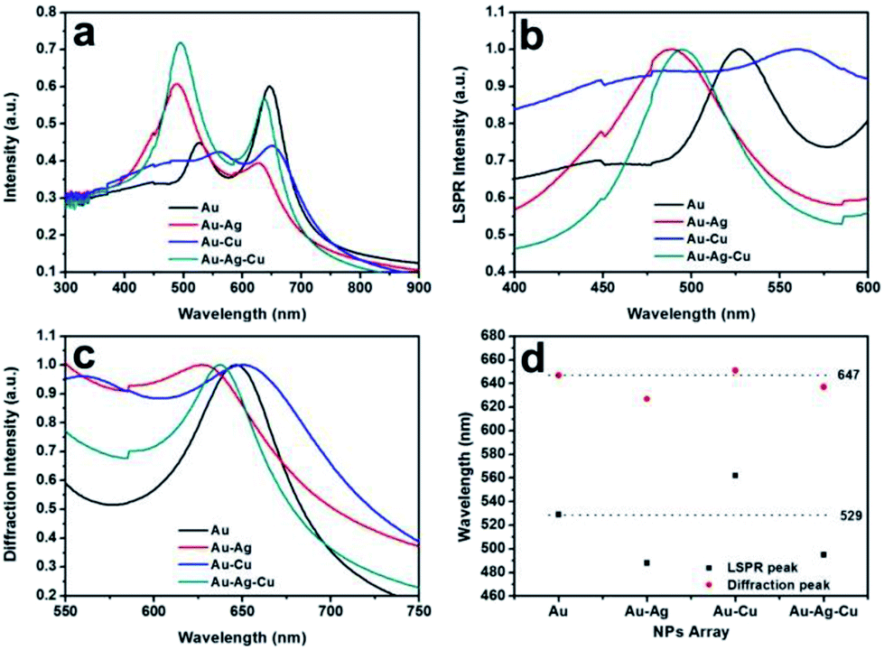 | ||
| Fig. 4 Full extinction spectra (a), LSPR spectra (b) and diffraction spectra (c) of Au, Au–Ag, Au–Cu and Au–Ag–Cu NPs array obtained by colloidal monolayer with periodic length of 500 nm on quartz sheet; (d) value of LSPR and diffraction peaks of Au, Au–Ag, Au–Cu and Au–Ag–Cu NPs array. | ||
The diffraction peaks of the Au, Au–Ag, Au–Cu and Au–Ag–Cu NPs array had a similar change trend to their LSPR peaks. The diffraction peak of the Au NPs array centered at 647 nm was measured. The Au–Ag alloyed NPs had a diffraction peak at 627 nm, which blue shifted by ca. 20 nm relative to the peak for pure Au NPs array. However, the diffraction peak of Au–Cu NPs array (ca. 651 nm) was only slightly red shifted by ca. 4 nm relative to the peak of pure Au NPs array. The diffraction peak of the Au–Ag–Cu NPs array was located at ca. 637 nm, which was between the diffraction peak positions of the Au–Ag and Au–Cu NPs array. Additionally, Fig. 4d shows points of LSPR and diffraction peaks. It indicated the LSPR peak is more sensitive to composition change of the noble-metal NPs than the diffraction peak. Thus, the LSPR absorption peak and the diffraction peak of noble-metal NPs array could be tuned by varying composition of the metal NPs without changing the periodicity of array.
4. Mechanism
4.1 Formation of hexagonal periodic ternary alloyed particle arrays by thermal annealing treatment
PS microspheres are apt to form monolayer colloidal crystals with hexagonal close-packed (hcp) arrangements by a self-assembling method at the air–water interface, because an hcp structure is a thermodynamically stable 2D arrangement with the minimum free energy for monodispersed isotropic colloidal spheres.29,30 In the preparation process of NPs array, the as-fabricated monolayer colloidal crystals were served as deposition template (Fig. 5a), followed by sputtering deposition. During sputtering deposition process, individual atoms and clusters of atoms ejected from the Au target reached to bending surface of the colloidal spheres of the template with multiple directions and then condensed on them. Small NPs with several tens of nanometers were formed on the template at the first stage, and then densely packed nanocolumn structures were appeared on the top surface along the colloidal sphere normal direction due to multiple-direction deposition and atomic shadow effect among these NPs formed at the first stage.31−33 With increase of deposition time, Au film became thicker on the top surfaces and some materials gradually extend to the lower part surface of colloidal spheres as well as the interstice of three adjacent colloidal spheres, as shown in Fig. 5b and c. Consequently, monolayer colloidal spheres turns into ordered arrays with structural units of egg-like shape.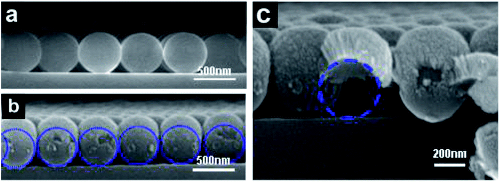 | ||
| Fig. 5 SEM images of Au film with nanocolumn structures formed on the top surface of colloidal spheres along their normal direction after magnetron sputtering deposition observed from cross-sectional view. (a) Low-magnification image before deposition Au film; (b) low-magnification image after deposition Au film; (c) corresponding expanded image of (b). | ||
With annealing temperature upon 1000 °C, which is much higher than thermal decomposition temperature (Td: ca. 400 °C) of PS, the PS spheres disappeared gradually due to the formation of volatile products, such as CO2 and H2O, which were easily desorbed from the substrates. Consequently, Au film deposited on the surface of PS spheres collapsed into bottom in situ on quartz substrate. Although the melting point of bulk gold rose as high as 1064 °C, low-dimensional nanoscaled Au materials possess much lower melted point. When the heating temperature was above 500 °C, the Au film composed of packed nanocolumn structures and particle-like fragments began to melt gradually. Subsequently, when the heating temperature rose upon to 1000 °C, all the Au film melted sufficiently. The melted Au materials did not wet the surface of quartz wafers, and tended to migrate toward dot centers and necessarily agglomerated together,34−36 leaving a non-coated space between the dots. There were more Au materials on the PS top surfaces than other places, so the Au NP positioned at centred place of PS was bigger than others. Furthermore, the scattered small particles disappeared gradually due to migration and agglomeration with centered bigger NP, consequently, spherical liquid Au droplets were formed in situ below previous colloidal spheres on substrate surface, and the shape becomes more regular and much closer to sphere. After solidification, the Au spherical NPs formed in situ under previous colloidal spheres.
Where after, other metallic, such as Ag, Cu thin film was deposited on the surface using periodic Au spherical NPs arrays as the second deposition template by magnetron sputtering deposition technology. It is necessary to provide reducing atmosphere during annealing process because they are readily oxidized in oxygen atmosphere at high temperature. Similarly, silver or copper film was melt and tended to migrate toward pre-existing Au NPs during the annealing process in reducing atmosphere, (N2 (96%), H2 (4%), volume ratio) at 750 °C for 2 h. Both Ag and Cu have the same face-centered crystal structure as Au, and can form solid solution state with each other. Furthermore, the crystal lattice constant of Ag, Cu and Au is 0.40862, 0.40786 and 0.3615 nm, respectively. They tend to be alloying at high temperature due to small lattice mismatch and large atomic diffusion rate. Finally, ternary Au–Ag–Cu spherical ordered NPs arrays were obtained. Moreover, the obtained alloyed NPs with a good spherical shape showed a uniform size distribution and morphology benefited from large-scale monolayer closed colloidal template, as well as higher stability provided by physical vapour deposition.
4.2 Shift mechanism of LSPR and diffraction peaks
The LSPR peak of noble-metal NPs depends on size, shape, dielectric constant and the surrounding medium of the particle. The shift of diffraction peak of the ordered NPs array is caused by periodic length of array, angle of incident light, dielectric constant and surrounding medium of NPs. In our work, the periodicity of the array, the angle of incident light, surrounding medium (air) and shape of NPs were fixed.The variety of dielectric constant has an important influence on the LSPR peak and diffraction peak. And the LSPR peak and diffraction peak would blue or red shift with the decrease or increase dielectric constant. Thus, both the LSPR and diffraction peaks of Au–Ag alloyed NPs array blue shifted due to their lower dielectric constant compared with pure Au NPs. However, in comparison with Au element, Cu element possesses a higher dielectric constant, leading to the red shift of the LSPR and diffraction peaks of Au–Cu alloyed NPs array, as shown in Fig. 4.
Moreover, besides dielectric constant, the size of alloyed NPs also plays an important role in shift of LSPR and diffraction peaks. Au–Ag alloyed NPs arrays are considered here as an example. Firstly, ordered spherical Au NPs arrays are obtained by depositing Au film on colloidal monolayer crystal for 60 s followed by heating at 1000 °C for 2 h in a tube furnace. Then sphere-shaped Au–Ag NPs arrays with varying Ag content were formed by controlling deposition time of Ag film using periodic Au spherical NPs arrays as the second deposition template. As shown in Fig. 6, in images marked 6a-d, the deposing time of Ag film is 20, 30, 60 and 120 s, respectively. Consequently, The size of Au–Ag alloyed NPs is 199, 214, 263 and 281 nm, respectively.
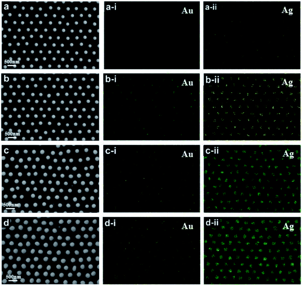 | ||
| Fig. 6 SEM images and corresponding EDS elemental distributing map of sphere-shaped Au–Ag NPs arrays with periodic length of 500 nm on quartz sheet with varying Ag content by controlling deposition time of Ag film using periodic Au spherical NPs arrays as the second deposition template; in images marked (a–d), the deposing time of Ag film is 20, 30, 60 and 120 s, respectively. | ||
The LSPR peak produced by Au positioned at 527 nm takes blue-shift to 498 due to the addition of Ag component (Fig. 7). Moreover, with increasing of Ag content, the peak further blue shift gradually to 479 nm. In addition, the intensity of the peak increases substantially. The diffraction peak blue shifts slightly from 642 to 633 due to the addition of Ag component. However, the peak shows obvious red shift from 633 to 708 nm with increasing of alloyed NPs size caused by the increase of Ag content. Additionally, Au–Cu alloyed NPs with varying Cu content were fabricated by controlling deposition time of Cu film also using periodic Au spherical NPs arrays as the second deposition template (Fig. S6†). The LSPR peak produced by Au positioned at 527 nm takes red-shift to 535 due to the addition of Cu component. Moreover, with increasing of Cu content, the peak further blue shifts gradually to 564 nm. The diffraction peak red shift slightly from 637 to 664 due to the increased size of alloyed NPs resulting from the increased Cu content (Fig. S7†).
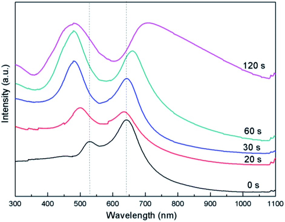 | ||
| Fig. 7 Extinction spectrum of Au–Ag alloyed NPs arrays with different sizes caused by depositing increasing time of Ag film using periodic Au spherical NPs arrays as the second deposition template. | ||
5. Conclusions
Large-area ordered Au–Ag, Au–Cu, Au–Ag–Cu NPs arrays with controllable composition, size and center-to-center spacing are fabricated by physical vapour deposition of metal on monolayer colloidal crystal template, followed by heat treatment. The composition and center-to-center spacing were manipulated by adjusting the sputtering target in deposition process and the size of colloidal spheres of the template, respectively. The alloyed NPs arrays exhibit hexagonal non-closed arrangement and possess face-centred-cubic structure. The LSPR peak of Au–Ag alloyed NPs blue shifted by ca. 40 nm and the LSPR peak of Au–Cu alloyed NPs array red shifted by ca. 34 nm relative to the peak for pure Au NPs array. The LSPR peak of Au–Ag–Cu alloyed NPs array with a LSPR absorption peak at wavelengths was at ca. 495 nm, between the LSPR peak Au–Ag and Au–Cu alloyed NPs array. The diffraction peaks of the Au–Ag, Au–Cu and Au–Ag–Cu NPs array had a similar change trend as their LSPR peaks, but less sensitive to composition change of the noble-metal NPs than the LSPR peaks. The variety of the LSPR peak and diffraction peak of the alloyed NPs array depends on the change of dielectric constant and the size of NPs. This work would open up a novel strategy in the production of alloyed NPs arrays with tunable LSPR peak and diffraction peak, which would be highly helpful to improve their practical applications in various fields.Conflicts of interest
There are no conflicts to declare.Acknowledgements
The authors acknowledge the financial support from the Natural Science Foundation of China (51701054), the education program of outstanding engineers in Jiangxi province (201417), the Scientific Research Foundation of Jiangxi Provincial Education Department (GJJ150811), Initial Scientific Research Foundation of doctor in Jiangxi Science and Technology Normal University (3000990339).Notes and references
- F. A. A. Nugroh, B. Iandolo, J. B. Wagner and C. Langhammer, ACS Nano, 2016, 10, 2871–2879 CrossRef PubMed
.
- W. Ingram, S. Larson, D. Carlson and Y. P. Zhao, Nanotechnology, 2017, 28, 015301 CrossRef PubMed
- N. S. Kanhe, A. K. Tak, A. B. Nawale, S. A. Raut, S. V. Bhoraskar, A. K. Das and V. L. Mathe, Mater. Des., 2016, 112, 495–504 CrossRef CAS
- M. Koike, D. Li, H. Watanabe, Y. Nakagawa and K. Tomishige, Appl. Catal., A, 2015, 506, 151–162 CrossRef CAS
- B. C. Marin, J. Ramĺrez, S. E. Root, E. Aklile and D. J. Lipomi, Nanoscale Horiz., 2017, 2, 311–318 RSC
- J. K. Nørskov, T. Bligaard, J. Rossmeisl and C. H. Christensen, Nat. Chem., 2009, 1, 37–46 CrossRef PubMed
- S. Jahn, S. J. Lechner, H. Freichels, M. Möller and J. P. Spatz, Sci. Rep., 2016, 6, 20536 CrossRef CAS PubMed
- N. E. Motl, E. Ewusi-Annan, I. T. Sines, L. Jensen and R. E. Schaak, J. Phys. Chem. C, 2010, 114, 19263–19269 CAS
- T. W. Chang, M. R. Gartia, S. Seo, A. Hsiao and G. L. Liu, Nanotechnology, 2014, 25, 145304 CrossRef PubMed
- Y. G. Sun and Y. N. Xia, Science, 2002, 298, 2176–2179 CrossRef CAS PubMed
- L. F. Hang, F. Zhou, D. D. Men, H. L. Li, X. Y. Li, H. H. Zhang, G. Q. Liu, W. P. Cai, C. C. Li and Y. Li, Nano Res., 2017, 10, 2257–2270 CrossRef CAS
- M. P. Mallin and C. J. Murphy, Nano Lett., 2002, 2, 1235–1237 CrossRef CAS
- C. Wang, H. Yin, R. Chan, S. Peng, S. Dai and S. Sun, Chem. Mater., 2009, 21, 433–435 CrossRef CAS
- Q. C. Dong, W. S. Qu, W. Q. Liang, K. P. Guo, H. B. Xue, Y. Y. Guo, Z. G. Meng, C. L. Ho, C. W. Leung and W. Y. Wong, Nanoscale, 2016, 8, 7068–7074 RSC
- Q. C. Dong, G. J. Li, C. L. Ho, M. Faisal, C. W. Leung, P. W. Pong, K. Liu, B. Z. Tang, I. Manners and W. Y. Wong, Adv. Mater., 2012, 24, 1034–1040 CrossRef CAS PubMed
- S. Liu, G. Y. Chen, P. N. Prasad and M. T. Swihart, Chem. Mater., 2011, 23, 4098–4101 CrossRef CAS
- A. Q. Gao, W. J. Xu, Y. P. D. León, Y. C. Bai, M. F. Gong, K. L. Xie, B. H. Park and Y. D. Yin, Adv. Mater., 2017, 29, 1701070 CrossRef PubMed
- K. Liu, Y. C. Bai, L. Zhang, Z. B. Yang, Q. K. Fan, H. Q. Q Zheng, Y. D. Yin and C. B. Gao, Nano Lett., 2016, 16, 3675–3681 CrossRef CAS PubMed
- T. T. Zheng, G. G. Li, F. Zhou, R. Wu, J. J. Zhu and H. Wang, Adv. Mater., 2016, 28, 8218 CrossRef CAS PubMed
- G. G. Li, E. Villarreal, Q. F. Zhang, T. T. Zheng, J. J. Zhu and H. Wang, ACS Appl. Mater. Interfaces, 2016, 8, 23920 CAS
- D. D. Men, F. Zhou, L. F. Hang, X. Y. Li, G. T. Duan, W. P. Cai and Y. Li, J. Mater. Chem. C, 2016, 4, 2117–2122 RSC
- Y. Q. Sun, L. F. Hang, D. D. Men, H. L. Li, D. L. Liu, X. Y. Li, L. L. Wen and Y. Li, J. Mater. Chem. C, 2016, 4, 9864–9871 RSC
- L. F. Hang, Y. Zhao, H. H. Zhang, G. Q. Liu, W. P. Cai, Y. Li and L. T. Qu, Acta Mater., 2016, 105, 59–67 CrossRef CAS
- M. Valodkar, S. Modi, A. Pal and S. Thakore, Mater. Res. Bull., 2011, 46, 384–389 CrossRef CAS
- H. H. Zhang, M. Liu, F. Zhou, D. L. Liu, G. Q. Liu, G. T. Duan, W. P. Cai and Y. Li, Small, 2015, 11, 844–853 CrossRef CAS PubMed
- Z. Z. Gu, R. Horie, S. Kubo, Y. Yamada, A. Fujishima and O. Sato, Angew. Chem., Int. Ed., 2002, 41, 1154–1156 Search PubMed
- S. Link, Z. L. Wang and M. A. El-Sayed, J. Phys. Chem. B, 1999, 103, 3529–3533 CrossRef CAS
- D. D. Men, F. Zhou, H. L. Li, L. F. Hang, X. Y. Li, D. L. Liu, W. P. Cai and Y. Li, J. Mater. Res., 2017, 32, 717–725 CrossRef CAS
- J. H. Zhang, Y. F. Li, X. M. Zhang and B. Yang, Adv. Mater., 2010, 22, 4249 CrossRef CAS PubMed
- X. Z. Ye and L. M. Qi, Nano Today, 2011, 6, 608–631 CrossRef CAS
- M. J. Brett and M. M. Hawkeye, Science, 2008, 319, 1192–1193 CrossRef CAS PubMed
- S. Mukherjee and D. Gall, J. Appl. Phys., 2010, 107, 084301 CrossRef
- H. H. Zhang, F. Zhou, M. Liu, D. L. Liu, D. D. Men, W. P. Cai, G. T. Duan and Y. Li, Adv. Mater. Interfaces, 2015, 2, 1500031 CrossRef
- Y. K. Lin, H. W. Ting, C. Y. Wang, S. Gwo, L. J. Chou, C. J. Tsai and L. J. Chen, Nano Lett., 2013, 13, 2723–2731 CrossRef CAS PubMed
- K. K. Nanda, S. N. Sahu and S. N. Behera, Phys. Rev. A, 2002, 66, 013208 CrossRef
- Y. Y. Wu, N. Y. Dong, S. F. Fu, J. D. Fowlkes, L. Kondic, M. A. Vincenti, D. D. Ceglia and P. D. Rack, ACS Appl. Mater. Interfaces, 2014, 6, 5835–5843 CAS
Footnote |
| † Electronic supplementary information (ESI) available. See DOI: 10.1039/c7ra13567j |
| This journal is © The Royal Society of Chemistry 2018 |