
 Open Access Article
 This Open Access Article is licensed under a
 Creative Commons Attribution 3.0 Unported Licence
Interface engineering of graphene–silicon Schottky junction solar cells with an Al2O3 interfacial layer grown by atomic layer deposition
Aaesha
Alnuaimi
 *ab,
Ibraheem
Almansouri
b,
Irfan
Saadat
b and
Ammar
Nayfeh
b
*ab,
Ibraheem
Almansouri
b,
Irfan
Saadat
b and
Ammar
Nayfeh
b
aResearch and Development Centre, Dubai Electricity and Water Authority (DEWA), Dubai, United Arab Emirates
bDepartment of Electrical and Computer Engineering (ECE), Masdar Institute, Khalifa University of Science and Technology, P. O. Box 54224, Abu Dhabi, United Arab Emirates. E-mail: aar.alnuaimi@gmail.com
First published on 16th March 2018
Abstract
The recent progress in graphene (Gr)/silicon (Si) Schottky barrier solar cells (SBSC) has shown the potential to produce low cost and high efficiency solar cells. Among the different approaches to improve the performance of Gr/Si SBSC is engineering the interface with an interfacial layer to reduce the high recombination at the graphene (Gr)/silicon (Si) interface and facilitate the transport of photo-generated carriers. Herein, we demonstrate improved performance of Gr/Si SBSC by engineering the interface with an aluminum oxide (Al2O3) layer grown by atomic layer deposition (ALD). With the introduction of an Al2O3 interfacial layer, the Schottky barrier height is increased from 0.843 V to 0.912 V which contributed to an increase in the open circuit voltage from 0.45 V to 0.48 V. The power conversion efficiency improved from 7.2% to 8.7% with the Al2O3 interfacial layer. The stability of the Gr/Al2O3/Si devices was further investigated and the results have shown a stable performance after four weeks of operation. The findings of this work underpin the potential of using an Al2O3 interfacial layer to enhance the performance and stability of Gr/Si SBSC.
1. Introduction
The high cost and inadequate efficiency of existing solar cell technologies have caused current efforts to focus on investigating new materials to achieve low cost and high efficiency solar cells. Graphene is one of the most promising materials that has attracted a tremendous amount of attention in the photovoltaics field due to its unique properties, being a two-dimensional material with near-zero bandgap and highly transparent film with excellent electrical conductivity. Graphene has been utilized in various PV technologies as a transparent electrode, electron and hole transport layer in organic solar cells and catalyst in dye sensitized solar cells (DSSCs).1–8 The recent development of Gr/silicon (Si) Schottky barrier solar cells (SBSC) have shown a great potential to produce low cost and high efficiency solar cells with the highest reported efficiency being 15.6%.9,10 Despite the recent efforts in enhancing the electrical and optical performance of Gr/Si SBSC,9–23 further performance optimization is required. The performance of Gr/Si SBSC is highly affected by the high recombination at Gr/Si interface and the continues but non-uniform growth of native oxide that prevents the tunnelling of the photo-generated charge carriers and leading to performance degradation and instability issues. Such behaviour has been observed for metal/Si interface and among the different approaches that have been adopted to reduce the recombination and enhance the interface properties is engineering the interface with interfacial layers.24–27 Previous studies on Gr/Si SBSC have shown an improved performance of Gr/Si SBSC by introducing solution based interfacial layers to improve Gr/Si interface.15,18,19,21,22 However, some of the undesirable properties of solution processed materials are the difficulty in obtaining uniform coating and controlling the thickness precisely which are important properties to obtain good passivation at the interface that doesn't affect the tunnelling of the charge carriers. The ALD technique is an excellent choice for the deposition of high quality thin film owning to the ability of obtaining conformal coating and controlling the thickness and composition at the atomic level. Herein, we analyzed the effect of Al2O3 grown by ALD as interfacial layer for Gr/Si SBSC.2. Experimental methods
2.1 Graphene synthesis
A high quality monolayer graphene with sheet resistance of ∼650 Ω sq−1 was grown on copper foil using chemical vapour deposition using Aixtron cold wall CVD reactor. The growth was done using a mixture of methane CH4 (15 sccm) and hydrogen H2 (60 sccm) at 1060 °C and pressure of 15 mbar. Further details about the synthesis can be found in ref. 28. The formation of high quality monolayer graphene was examined using Raman analysis. Fig. 1 shows the Raman spectrum of as-synthesized graphene. The ratio of 2D-band peak (2682 cm−1) to G-band-peak (1580 cm−1) I2D/IG is greater than two which confirms the formation of a monolayer graphene. The weak D-band peak (1350 cm−1) suggests the high quality of the grown graphene.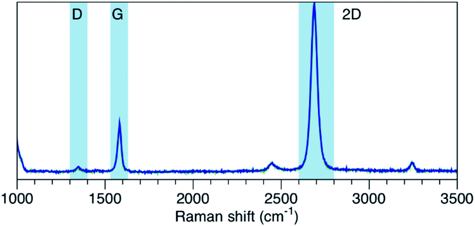 | ||
| Fig. 1 Raman spectrum of synthesized graphene.28 | ||
2.2 Gr/Si solar cells fabrication
The fabrication steps of Gr/Si SBSC are illustrated in Fig. 2. Twelve solar cells with active area of 2 × 2 mm were fabricated using lightly doped n-type Si substrate with resistivity of 3–4 Ω cm. A 300 nm silicon oxide was deposited on top of the silicon substrate to define the active area. Using lithography, a window was patterned and the silicon oxide was etched using buffered oxide etch (BOE) to expose the underlying silicon which defines the size of the solar cell. After the etching step, the samples were transferred to the Oxford instruments FlexAl ALD reactor for Al2O3 deposition.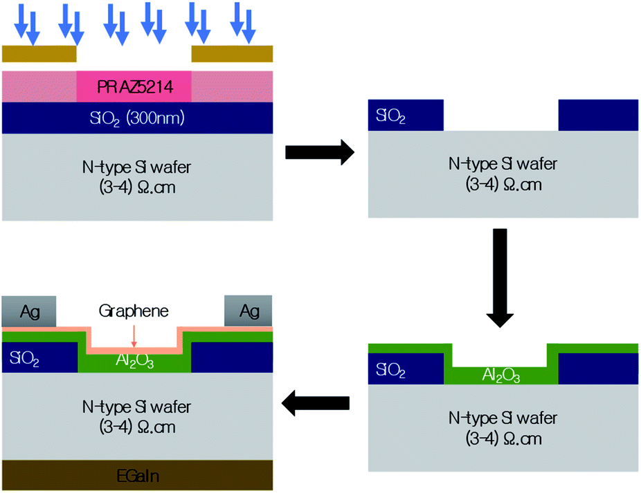 | ||
| Fig. 2 Schematic diagram of Gr/Al2O3/Si solar cell fabrication steps. | ||
A thin layer of Al2O3 oxide was deposited using thermal ALD at low temperature of 300 °C and pressure of 200 mTorr. Trimethylaluminum (TMA, Al(CH3)3) was used as the gas precursor for Al while H2O is used the oxygen precursor. The estimated deposition rate is 1 Å per cycle and the estimated thickness is ∼20 Å. The ALD step was followed by graphene transfer. Two layers of graphene were transferred using the standard PMMA (poly(methyl methacrylate)) transfer process. The samples were exposed to the vapour of nitric acid for 1 min to dope the graphene. Gallium–indium eutectic (Ga–In 99.99%) was used as the back silicon contact while silver (Ag) paste was applied around the active area to contact the graphene.
2.3 Gr/Si solar cells characterization
Sol3A 94123A solar simulator was used to measure the current–voltage characteristics of the fabricated cells under 1 sun illumination. A black tape was used to cover the solar cell except at the active area to avoid any current collected from surrounding area. The light intensity of the simulator was calibrated using silicon reference cell and irradiance monitor. Agilent Probe analyser was used for the dark current measurements.3. Results and discussion
Fig. 3 illustrates the current density–voltage (J–V) curves under AM1.5 illumination conditions of Gr/Si solar cells with and without Al2O3 interfacial layer. In the absence of Al2O3 interfacial layer, the short circuit current density (Jsc), open circuit voltage (Voc) and fill factor (FF) of Gr/Si solar cell are 27.7 mA cm−2, 0.45 V, 58.3%. With the introduction of Al2O3 interfacial layer, the performance of the cell improved significantly. The Jsc, Voc, and FF increased to 28.8 mA cm−2, 0.48 V, 63.75% leading to an enhancement in the power conversion efficiency from 7.2% to 8.7%. Table 1 shows the average value of performance parameters of devices fabricated with and without Al2O3 passivation layer. Fig. 4 shows the histogram of keys performance parameters (Voc, Jsc, FF and PCE) for Gr/Si solar cells with Al2O3 interfacial layer.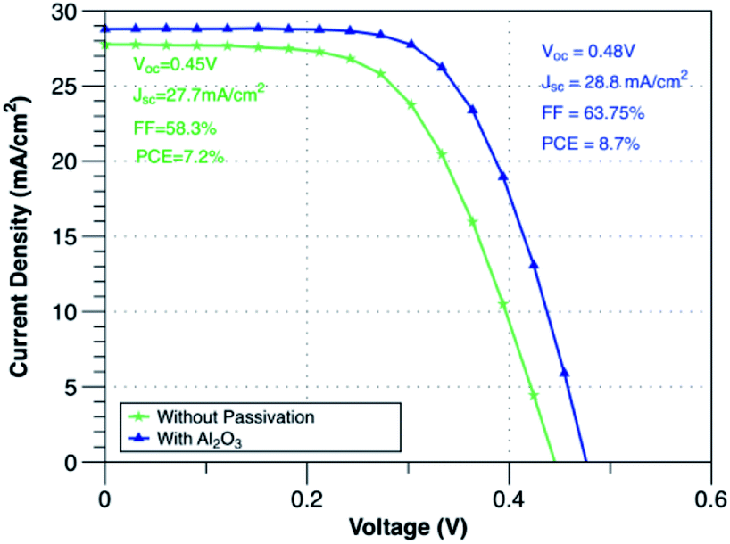 | ||
| Fig. 3 J–V characteristics of Gr/Si solar cells with and without Al2O3 interfacial layer. | ||
| Solar cell | V oc (V) | J sc mA cm−2 | FF (%) | PCE (%) |
|---|---|---|---|---|
| Without passivation | 0.43 | 27.7 | 53.9 | 6.4 |
| With Al2O3 | 0.47 | 28.6 | 59.2 | 8.0 |
 | ||
| Fig. 4 Histogram of (a) open circuit voltage (b) short circuit current (c) fill factor (d) power conversion efficiency for Gr/Si solar cells with Al2O3 interfacial layer. | ||
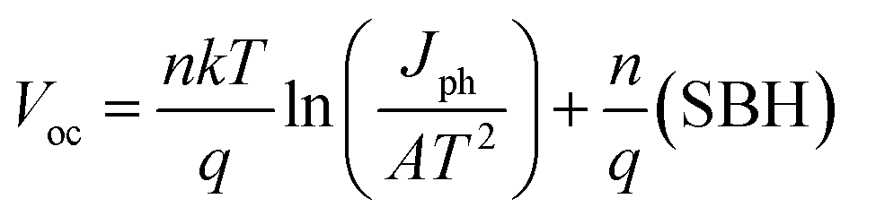
One of the main factors that contributed to the improvement in the solar cell performance with the addition of Al2O3 interfacial layer is the increase in the Schottky barrier height (SBH). The SBH was extracted from the slope of the dark ln(J)–V curve at the forward bias linear region as illustrated in Fig. 3a. For Gr/Si solar cells without Al2O3, the estimated SBH is 0.843 V and it increased to 0.921 V with Al2O3 interfacial layer. The increase in the barrier height at the interface blocks the transport of the photo-generated electrons in silicon hence reducing the leakage current. As illustrated in Fig. 5a, the reverse saturation current is reduced from 4.50 × 10⁻⁴ mA cm−2 to 4.48 × 10⁻⁵ mA cm−2 while the ideality factor (n) is reduced from 1.39 to 1.25 confirming the significant reduction in the recombination of carriers. Furthermore, the increase in the SBH also indicates the creation of larger built-in potential (Vbi) across the depletion region that is beneficial for enhancing the transfer of the carriers at the interface. The Vbi of the solar cell has been extracted from the crossover between the IV characteristics under illumination and dark condition29 and it was found that Vbi increased from 0.54 V to 0.58 V with Al2O3. The strong dependence of Voc on the SBH as described in eqn (1) as well as the reduction in the dark current and ideality factor clearly explains the increase in the Voc with the introduction of Al2O3 interfacial layer.
 | (1) |
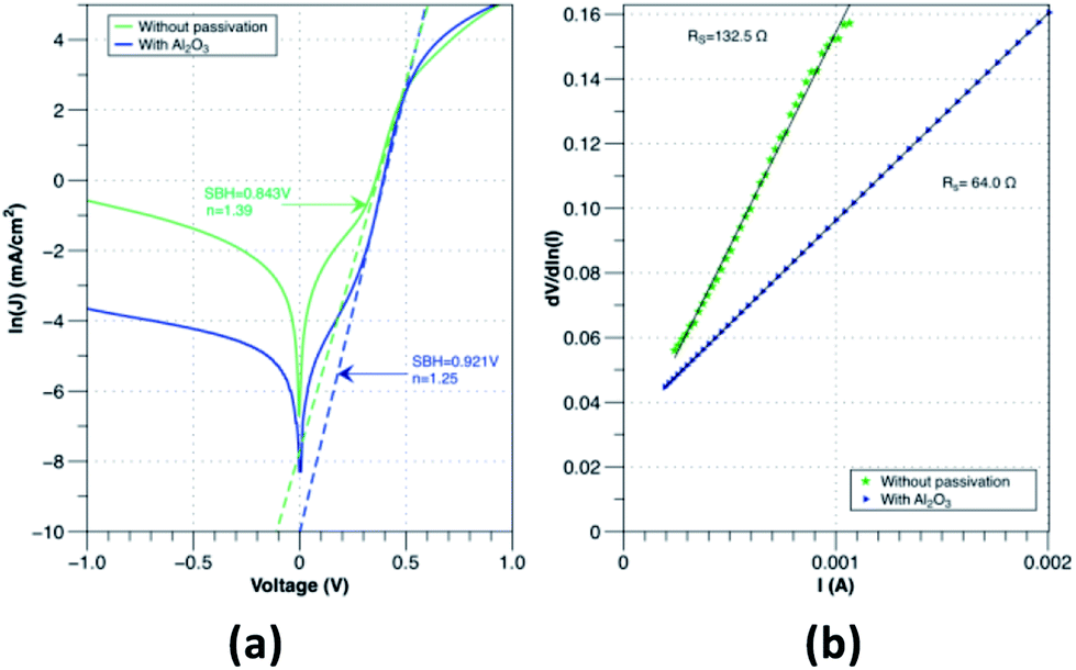 | ||
Fig. 5 (a) Dark J–V characteristics of Gr/Si solar cells with and without Al2O3 interfacial layer. Inset shows the corresponding ln![[thin space (1/6-em)]](https://www.rsc.org/images/entities/char_2009.gif) J–V curves. (b) Plots of dV/dln(I) versus I for Gr/Si solar cells with and without Al2O3 interfacial layer. J–V curves. (b) Plots of dV/dln(I) versus I for Gr/Si solar cells with and without Al2O3 interfacial layer. | ||
In addition, the series resistance Rs was extracted by plotting the curve of dV/dln(I) as a function of I and estimating the Rs value from the slope of the linear fitting to the curves to the curves (Fig. 5b). The series resistance dropped from 132.5 Ω to 64.0 Ω which results in improving the fill factor with Al2O3 interlayer.
The benefits of Al2O3 interfacial layers is not only limited to creating higher Schottky barrier but it also reduces the recombination at the interface. In SBSC the tunnelling of holes should dominates over the recombination to achieve effective charge carrier transport. According to Song et al.9 the existence of ultra-thin layer of native oxide passivates the interface between the graphene and silicon and allows the tunnelling of holes. However, since the native oxide thickness tends grow continuously, the performance of Gr/Si solar cell degrades with time. As shown in Fig. 6a, due to the increase in the native oxide thickness, the tunnelling of holes is reduced causing accumulation at the interface which consequently results in higher recombination of charge carriers. Therefore, the use of SiO2 interfacial layer has major issues that affect the performance stability of the Gr/Si SBSC. In contrast, Al2O3 has been proven as a good passivation layer for Si substrate.30–33 As shown in Fig. 6b, passivating the surface with Al2O3 immediately after the native oxide etch prevents the formation of thick native oxide at the interface. In addition, it creates a uniform and conformal Al2O3 layer that passivates the Si surface effectively. The formation of uniform ultra-thin Al2O3 layer contributed to reducing the surface recombination, improving the carrier lifetime for Si substrate and reducing the series resistance. According to Hoex et al.30 passivating the Si surface with Al2O3 reduces the density of traps significantly causing a major reduction in the surface recombination. Therefore, the enhancement of the solar cell performance with Al2O3 interfacial layer is mainly attributed to passivating the silicon surface that reduces the surface recombination and the creation of higher SBH that facilitates the transport of charge carrier effectivity.
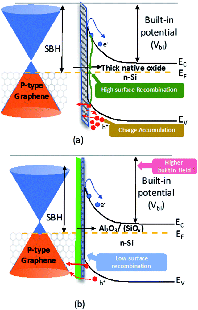 | ||
| Fig. 6 Energy band diagrams of Gr/Si SBSC (a) with thick interfacial layer (b) with Al2O3/native oxide interfacial layers. | ||
The stability of the cell was examined over four weeks as shown in Fig. 7. There was an observed degradation in the performance of the cell after one week. The drop in the efficiency and Voc after one week is mainly attributed to the degradation effect of nitric acid dopant as observed by Cui et al.13 The nitrite anions in nitric acid acts as a p-type dopant to the graphene (i.e. increasing the work function of the graphene) and reduces its sheet resistance. Upon the degradation of the dopant, the graphene work function decreases and the sheet resistance increases which results in a large drop in the efficiency and Voc.
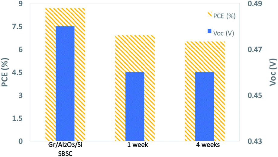 | ||
| Fig. 7 Variation of PCE and Voc of Gr/Si with Al2O3 interfacial layer over time. | ||
After four weeks, there was no observed major degradation in the cell performance. This highlights the benefit of using Al2O3 as a passivation layer and blocking layer since it prevents further growth of native oxide and helps the cell to maintain its performance. The slight reduction in the PCE from 6.9% in week 1 to 6.6% in week 4 is mainly attributed to the reduction in FF from 54.12% to 52.10%. The contact series resistance increased due to the use of silver paste as the top contact. The silver paste degrades more compared to thermally vacuum evaporated front contacts which mainly impact the series resistance and causes a reduction in the fill factor of the cell.34
Possible routes to further improve the efficiency of Gr/Si SBSC with Al2O3 layer is to investigate the effect of Al2O3 oxide and find the optimal thickness that maximize the cell efficiency. According to Song et al.9 increasing the interfacial layer thickness can further reduce the leakage current and contributes to increasing the Voc. However, with further increase in the interfacial layer beyond the optimal thickness, the tunnelling probability is reduced by the factor exp(−√χd) where χ is the average potential barrier of the oxide for hole tunnelling into the graphene and d is the interfacial layer thickness. Due to the reduction in the tunnelling probability, the charge carriers accumulate at the interface and results in increasing the recombination rate.
4. Conclusions
In conclusion, the use of Al2O3 interfacial layer to engineer the interface between the graphene and silicon is demonstrated. The existence of Al2O3 interfacial layer mainly contributed to increasing the open circuit voltage and fill factor. Al2O3 interfacial layer resulted in creating higher Schottky barrier height that is beneficial to increase the built-in potential and reduce recombination of charge carriers and leakage current. Solar cells with Al2O3 showed an improvement in the power conversion efficiency from 7.2% to 8.7% and good stability over four weeks. The results highlight the potential of using Al2O3 as interfacial layer for Gr/Si SBSC.Conflicts of interest
There are no conflicts to declare.Acknowledgements
The authors would like to acknowledge the valuable advice and constructive comments of Prof. Jing Kong and Yi-Song (from Massachusetts Institute of Technology) in graphene transfer as well as the fabrication of Gr/Si SBSC. This work is fully supported by Masdar Institute (part of Khalifa University of Science and Technology).References
- W. Hong, Y. Xu, G. Lu, C. Li and G. Shi, Transparent graphene/PEDOT-PSS composite films as counter electrodes of dye-sensitized solar cells, Electrochem. Commun., 2008, 10(10), 1555–1558 CrossRef CAS.
- Z. Liu, J. Li, Z.-H. Sun, G. Tai, S.-P. Lau and F. Yan, The application of highly doped single-layer graphene as the top electrodes of semitransparent organic solar cells, ACS Nano, 2011, 6(1), 810–818 CrossRef.
- H. Wang and Y. H. Hu, Graphene as a counter electrode material for dye-sensitized solar cells, Energy Environ. Sci., 2012, 5(8), 8182–8188 RSC.
- Y. Wang, S. W. Tong, X. F. Xu, B. Özyilmaz and K. P. Loh, Interface engineering of layer-by-layer stacked graphene anodes for high-performance organic solar cells, Adv. Mater., 2011, 23(13), 1514–1518 CrossRef CAS.
- D. Zhang, X. Li, H. Li, S. Chen, Z. Sun and X. Yin, et al. Graphene-based counter electrode for dye-sensitized solar cells, Carbon, 2011, 49(15), 5382–5388 CrossRef CAS.
- Y. Zhou, X. Xu, F. Hu, X. Zheng, W. Li and P. Zhao, et al. Graphene as broadband terahertz antireflection coating, Appl. Phys. Lett., 2014, 104(5), 051106 CrossRef.
- W. Yang, X. Xu, L. Hou, X. Ma, F. Yang and Y. Wang, et al. Insight into the topological defects and dopants in metal-free holey graphene for triiodide reduction in dye-sensitized solar cells, J. Mater. Chem. A, 2017, 5(12), 5952–5960 RSC.
- W. Yang, X. Xu, Y. Gao, Z. Li, C. Li and W. Wang, et al. High-surface-area nanomesh graphene with enriched edge sites as efficient metal-free cathodes for dye-sensitized solar cells, Nanoscale, 2016, 8(26), 13059–13066 RSC.
- Y. Song, X. Li, C. Mackin, X. Zhang, W. Fang and P. Ts, et al. Role of interfacial oxide in high-efficiency graphene–silicon Schottky barrier solar cells, Nano Lett., 2015, 15(3), 2104–2110 CrossRef CAS.
- X. Li, H. Zhu, K. Wang, A. Cao, J. Wei and C. Li, et al. Graphene-on-silicon Schottky junction solar cells, Adv. Mater., 2010, 22(25), 2743–2748 CrossRef CAS.
- X. Li, L. Fan, Z. Li, K. Wang, M. Zhong and J. Wei, et al. Boron Doping of Graphene for Graphene–Silicon p–n Junction Solar Cells, Adv. Energy Mater., 2012, 2(4), 425–429 CrossRef CAS.
- T. Feng, D. Xie, Y. Lin, H. Zhao, Y. Chen and H. Tian, et al. Efficiency enhancement of graphene/silicon-pillar-array solar cells by HNO3 and PEDOT-PSS, Nanoscale, 2012, 4(6), 2130–2133 RSC.
- T. Cui, R. Lv, Z.-H. Huang, S. Chen, Z. Zhang and X. Gan, et al. Enhanced efficiency of graphene/silicon heterojunction solar cells by molecular doping, J. Mater. Chem. A, 2013, 1(18), 5736–5740 RSC.
- Y. Tsuboi, F. Wang, D. Kozawa, K. Funahashi, S. Mouri and Y. Miyauchi, et al. Enhanced photovoltaic performances of graphene/Si solar cells by insertion of a MoS2 thin film, Nanoscale, 2015, 7(34), 14476–14482 RSC.
- K. Jiao, X. Wang, Y. Wang and Y. Chen, Graphene oxide as an effective interfacial layer for enhanced graphene/silicon solar cell performance, J. Mater. Chem. C, 2014, 2(37), 7715–7721 RSC.
- G. Fan, H. Zhu, K. Wang, J. Wei, X. Li and Q. Shu, et al. Graphene/silicon nanowire Schottky junction for enhanced light harvesting, ACS Appl. Mater. Interfaces, 2011, 3(3), 721–725 CrossRef CAS.
- X. Miao, S. Tongay, M. K. Petterson, K. Berke, A. G. Rinzler and B. R. Appleton, et al. High efficiency graphene solar cells by chemical doping, Nano Lett., 2012, 12(6), 2745–2750 CrossRef CAS.
- S. Lin, X. Li, P. Wang, Z. Xu, S. Zhang and H. Zhong, et al. Interface designed MoS2/GaAs heterostructure solar cell with sandwich stacked hexagonal boron nitride, Sci. Rep., 2015, 5, 15103 CrossRef CAS.
- L. Yang, X. Yu, M. Xu, H. Chen and D. Yang, Interface engineering for efficient and stable chemical-doping-free graphene-on-silicon solar cells by introducing a graphene oxide interlayer, J. Mater. Chem. A, 2014, 2(40), 16877–16883 RSC.
- X. Li, D. Xie, H. Park, M. Zhu, T. H. Zeng and K. Wang, et al. Ion doping of graphene for high-efficiency heterojunction solar cells, Nanoscale, 2013, 5(5), 1945–1948 RSC.
- K. Jiao, C. Duan, X. Wu, J. Chen, Y. Wang and Y. Chen, The role of MoS2 as an interfacial layer in graphene/silicon solar cells, Phys. Chem. Chem. Phys., 2015, 17(12), 8182–8186 RSC.
- C. Xie, X. Zhang, Y. Wu, X. Zhang, X. Zhang and Y. Wang, et al. Surface passivation and band engineering: a way toward high efficiency graphene–planar Si solar cells, J. Mater. Chem. A, 2013, 1(30), 8567–8574 RSC.
- Y. Li, W. Yang, Z. Tu, Z. Liu, F. Yang and L. Zhang, et al. Schottky junction solar cells based on graphene with different numbers of layers, Appl. Phys. Lett., 2014, 104(4), 043903 CrossRef.
- D. Lillington and W. Townsend, Effects of interfacial oxide layers on the performance of silicon Schottky-barrier solar cells, Appl. Phys. Lett., 1976, 28(2), 97–98 CrossRef CAS.
- Photocurrent suppression and interface state recombination in MIS-Schottky barriers, 1977 International Electron Devices Meeting, ed. Ng K. and Card H., 1977, pp. 57–61 Search PubMed.
- P. Viktorovitch and G. Kamarinos, Improvement of the photovoltaic efficiency of a metal-insulator-semiconductor structure: influence of interface states, J. Appl. Phys., 1977, 48(7), 3060–3064 CrossRef.
- Determination of optimum parameters and characterization of MIS solar cells, 1977 International Electron Devices Meeting, ed. Viktorovitch P., Pananakakis G., Kamarinos G. and Basset R., 1977, pp. 62–62 Search PubMed.
- A. Alnuaimi, I. Almansouri, I. Saadat and A. Nayfeh, Toward fast growth of large area high quality graphene using a cold-wall CVD reactor, RSC Adv., 2017, 7(82), 51951–51957 RSC.
- J. E. Moore, S. Dongaonkar, R. V. K. Chavali, M. A. Alam and M. S. Lundstrom, Correlation of built-in potential and I–V crossover in thin-film solar cells, IEEE Journal of Photovoltaics, 2014, 4(4), 1138–1148 Search PubMed.
- B. Hoex, S. Heil, E. Langereis, M. Van de Sanden and W. Kessels, Ultralow surface recombination of c-Si substrates passivated by plasma-assisted atomic layer deposited Al2O3, Appl. Phys. Lett., 2006, 89(4), 042112 CrossRef.
- J. Schmidt, A. Merkle, R. Brendel, B. Hoex, M. Van De Sanden and W. Kessels, Surface passivation of high-efficiency silicon solar cells by atomic-layer-deposited Al2O3, Progress in photovoltaics: research and applications, 2008, 16(6), pp. 461–466 Search PubMed.
- J. Deckers, E. Cornagliotti, M. Debucquoy, I. Gordon, R. Mertens and J. Poortmans, Aluminum oxide-aluminum stacks for contact passivation in silicon solar cells, Energy Procedia, 2014, 55, 656–664 CrossRef CAS.
- J. Benick, B. Hoex, M. Van de Sanden, W. Kessels, O. Schultz and S. W. Glunz, High efficiency n-type Si solar cells on Al2O3-passivated boron emitters, Appl. Phys. Lett., 2008, 92(25), 253504 CrossRef.
- A. R. Jha, Solar cell technology and applications, CRC press, 2009 Search PubMed.
| This journal is © The Royal Society of Chemistry 2018 |