DOI:
10.1039/C7RA13428B
(Paper)
RSC Adv., 2018,
8, 5984-5991
Interface engineering through electron transport layer modification for high efficiency organic solar cells†
Received
18th December 2017
, Accepted 24th January 2018
First published on 5th February 2018
Abstract
In the present study, we have compared the device performance of poly[4,8-bis(5-(2-ethylhexyl)thiophen-2-yl)benzo[1,2-b;4,5-b′]dithiophene-2,6-diyl-alt-(4-(2-ethylhexyl)-3-fluorothieno[3,4-b]thio-phene-)-2-carb-oxylate-2-6-diyl)] (PTB7-Th):phenyl-C71-butyric acid methyl ester (PCBM) organic solar cells (OSCs) in an inverted geometry with ZnO, a bilayer of ZnO and Ba(OH)2 [ZnO/Ba(OH)2] and a nanocomposite of ZnO and Ba(OH)2 [ZnO:Ba(OH)2] as electron transport layers (ETLs). Our study reveals that the performance of the devices with the ZnO/Ba(OH)2 and ZnO:Ba(OH)2 nanocomposite as ETL supersedes that of devices with only ZnO as ETL. The plausible reasons for the improved performance of these devices are identified using morphological studies, contact angle measurements, X-ray photoelectron spectroscopy (XPS), ultraviolet photoelectron spectroscopy (UPS) and photo-electrochemical impedance spectroscopy (EIS) measurements. It is observed that films of ZnO/Ba(OH)2 and ZnO:Ba(OH)2 nanocomposites have a low work function and are slightly more smooth and hydrophobic than ZnO films. This might have suppressed the charge recombination and thereby improved the charge collection as has been confirmed by EIS measurements.
1. Introduction
Solution processed bulk-heterojunction organic solar cells (OSCs), which consist of a conjugated polymer as an electron donor and fullerene and/or polymer as an acceptor, are widely regarded as an emerging PV technology and offer many advantages such as mechanical flexibility, low-cost, light weight, low energy consuming roll-to-roll manufacturing process, etc.1–5 Over the years, to increase the power conversion efficiency (PCE) of OSCs, various strategies have been used. This includes designing and developing new donor and/or acceptor molecules having wide absorption spectra and/or employing various aspects of device and interface engineering such as use of solvent additives for photoactive layer processing, incorporation of metals, dielectric and/or semiconducting nanoparticles (NPs) in the photoactive layer, use of buffer layers like electron and/or hole transport layers, etc.6–12 It has been demonstrated in the past that the careful selection of electron and/or hole transport layers can improve the PCE by 2–3% for the same donor:acceptor bulk-heterojunction system.12–17
Till date several types of material and/or their nanocomposites have been used as an electron transport layers (ETLs).2,18–20 Among them the most preferred ones are solution processed metal oxides (MeOx) like ZnO, TiO2, ZrO2, etc.21–23 This is quite obvious as most of these MeOx offer good air-stability, high transparency to visible light, high electron affinity, and tuneable electrical and optical properties.24,25 However, being a solution processed and low temperature processed, these MeOx often digress from the properties of single crystals and as a result, many-a-times, it is observed that defect related energy levels or Schottky barriers form interfacial barriers.26 Besides MeOx, organic dipole layers such as conjugated polyelectrolytes (CPE),2,27–29 organic salts, zwitterions and cost effective poly(ethyleneimine) (PEI)19 or poly-(ethyleneimine)-ethoxylated (PEIE)20 does modify the work function and has been used an ETL. Most of them can simply be spin-coated in ambient atmosphere just like MeOx and helps in simplifying the fabrication method. However, the insulating nature of these types of materials often leads to high series resistance in a thick film and therefore the performance of devices was found to be highly sensitive to the thickness of these layers.30–32
To overcome these issues, in recent times, two alternate approaches which include use of bilayer structure such as MeOx/PEI (PEIE/PFN) and MeOx:PEI (PEIE/PFN) nanocomposite as an ETL have been studied.19,20,33,34 Although the bilayer structure improves the PCE of the devices, the high thickness sensitivity of performance caused by PEI (PEIE) still can't be solved.30–32 On the other hand, MeOx:PEI (PEIE/PFN) nanocomposite offers combined advantages such as the high charge carrier mobility of MeOx and good film formation ability of polymer.33–35 As a result, devices with nanocomposite as an ETL often demonstrate high PCE and good stability. Recently, less-studied type of inorganic salt, barium hydroxide [Ba(OH)2] has been explored as an ETL so as to improve device performance in polymer light-emitting diodes (PLEDs),36 organic field effect transistors (OFETs),37 OSCs owing to its outstanding charge injection ability. A remarkable enhancement in PCE of OSCs has been demonstrated by employing Ba(OH)2 as an ETL or upon inserting a Ba(OH)2 layer between photoactive layer and ETLs.26,38 Both this approaches contribute to reduction of energetic barrier at the interface and improves charge collection.
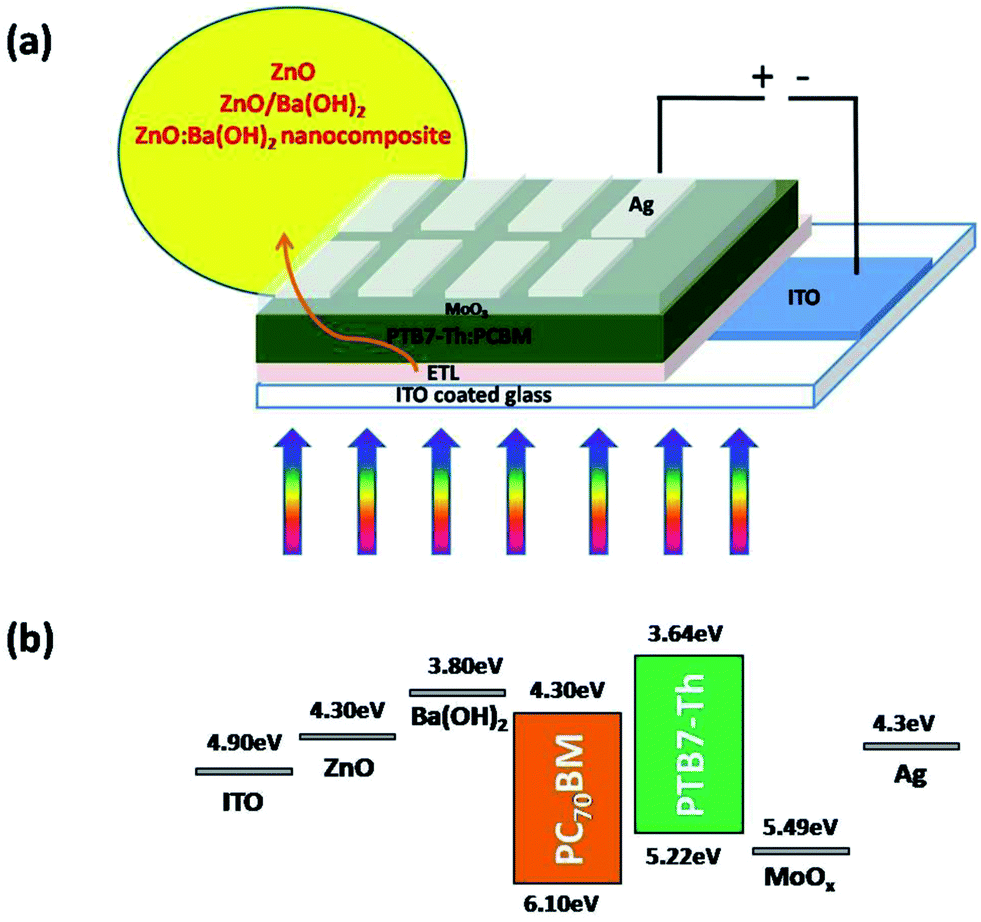
Here in, we have adopted a novel approach in which we have blended a sol–gel ZnO solution with a Ba(OH)2 solution prior to their final consolidation into the nanocomposite layer as the ETL. From the similar type of previous studies, we presume that the presence of Ba(OH)2 in ZnO might induce stronger electrostatic or dipole–dipole interactions with a ZnO surface and therefore use of ZnO:Ba(OH)2 nanocomposites as ETLs would improve the device performance of OSCs. Devices were fabricated in an inverted geometry having a structure ITO/ZnO or bilayer of ZnO and Ba(OH)2 [ZnO/Ba(OH)2] or nanocomposite of ZnO and Ba(OH)2 [ZnO:Ba(OH)2] nanocomposites (40 nm)/PTB7-Th:PCBM(100 nm)/MoO3 (10 nm)/Ag (100 nm). Our study reveals that the performance of the devices with ZnO/Ba(OH)2 and ZnO:Ba(OH)2 nanocomposite as ETL supersedes that of devices with only ZnO as ETL. The plausible reasons for the improved performance of these devices are identified using contact angle measurements, atomic force microscopy (AFM), X-ray photoelectron spectroscopy (XPS), ultraviolet photoelectron spectroscopy (UPS) and photo-EIS measurements.
2. Experimental
2.1 Preparation of sol gel ZnO
Sol gel ZnO was prepared by the method reported in our previous work.39 At first, equimolar (0.25 M) solution of zinc acetate dihydrate (Aldrich, 99.9%) and ethanolamine was prepared in 10 ml of 2-methoxy ethanol. Thereafter, solution was allowed to stir rigorously for 12 h at 70 °C to get a homogeneous, clear and transparent solution. Thereafter solution was aged for 24 h before using it for spin-coating as an electron transport layer.
2.2 Preparation of barium hydroxide solution
The barium hydroxide solution was prepared by dissolving barium hydroxide in 2-methoxyethanol (2 mg ml−1).26,38 The Ba(OH)2 solution was filtered by a nylon filter with a diameter of 0.45 μm prior to the spin-cast.
2.3 Preparation of zinc oxide/barium hydroxide nanocomposites
For preparation of ZnO:Ba(OH)2 nanocomposite, ZnO stock solution was mixed with a set amount of Ba(OH)2 solution (3, 6, 9 and 12 w/w%) and stirred vigorously for 12 h. As obtained solutions were filtered by a nylon filter with a diameter of 0.45 μm prior to the spin-cast.
2.4 Device fabrication
Devices were fabricated following the device architecture mentioned in the Fig. 1(a) and corresponding energy levels of the materials used in the fabrication are shown in the Fig. 1(b).38,39 At first, photoactive blend comprised of PTB7-Th (10 mg) and PCBM (15 mg) was prepared in 1 ml of DCB with 3% v/v of 1,8-diiodooctane (DIO) solvent as an additive. The solution was allowed to stir at 70 °C in the dark for at least 12 h. For the device fabrication, ITO coated glass substrates (Luminescence Technology corp. Taiwan, with a sheet resistance of 15 Ω sq−1 and transmittance > 85%) were cleaned by process reported in our previous work.7,40 For the devices with ZnO and ZnO:Ba(OH)2 nanocomposite as an ETL, ZnO and ZnO:Ba(OH)2 nanocomposite solutions which was previously synthesized, was spin-coated on pre-cleaned ITO substrates at 2000 rpm for 30 s to obtain a film of ∼40 nm. The substrates were then annealed at 200 °C for 15 min to remove excess solvents. Thereafter, substrates were transferred inside nitrogen filled glove box and a photoactive blend was spin-coated at 1100 rpm for 120 s. The films were allowed to get dried for 2 h and then subsequently, the devices were evaporated using the shadow mask by thermal evaporation of 10 nm MoO3 layer as a hole transport layer and 100 nm Ag electrode as anode. For the devices with ZnO/Ba(OH)2, an additional layer of Ba(OH)2 was spin-coated on the top of ZnO layer and allowed to dry before spin-coating the photoactive layer. Thereafter the film is annealed at 200 °C for 5 min to remove excess solvent if any.
 |
| | Fig. 1 (a) Schematic of PTB7-Th:PCBM OSCs in an inverted geometry with ZnO, ZnO/Ba(OH)2 and ZnO:Ba(OH)2 nanocomposite as ETLs (b) energy levels of materials used in the solar cell device. | |
2.5 Device characterization and testing
The current density–voltage (J–V) characteristics curves of fabricated devices were measured using a Keithley 2600 source meter and a Newport solar simulator (model number 91160) shines light with AM 1.5 G spectral distribution, which was calibrated using a certified reference solar cell to an intensity of 1000 W m−2. External quantum efficiency (EQE) spectra were obtained from Bentham's PVE300. The test cells were masked with a single aperture and care has been taken to exclude all light from entering the cell elsewhere, including shading of the edges of the substrates. The active device area is defined as 4.5 mm2 by using a shadow mask. Conductivity measurements of various ETLs were performed by Broadband Dielectric Spectroscopy at room temperature using Alpha-A high performance frequency analyser.
3. Results and discussion
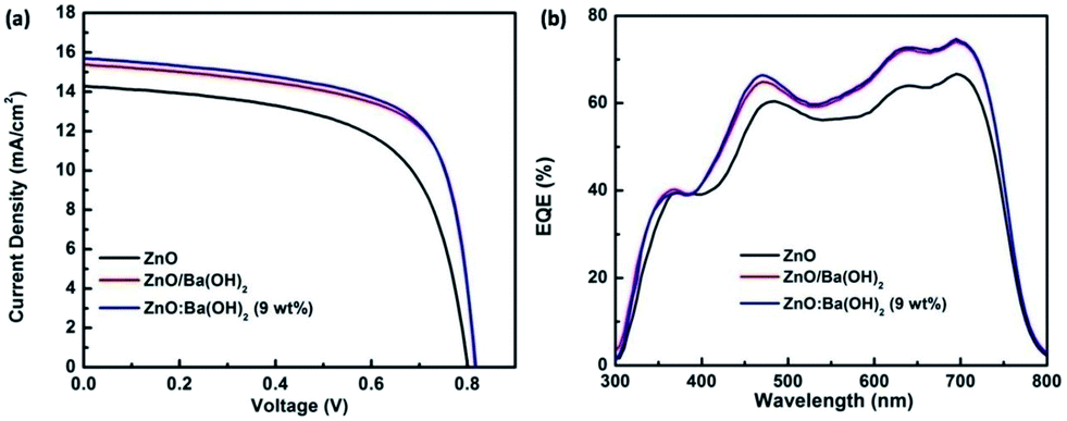
Fig. 2(a) and (b) presents the J–V characteristics curves and external quantum efficiency (EQE) spectra of devices with different ETLs. Photovoltaic parameters such as open circuit voltage (Voc), short-circuit current density (Jsc), fill factor (FF), and PCE for the devices with ZnO, ZnO/Ba(OH)2 and ZnO:Ba(OH)2 (9 wt%) nanocomposite as an ETL are shown in Table 1 and for all the fabricated devices are summarized in Table S1.† As can be seen, for the control device with only ZnO as an ETL, Voc, Jsc, FF and PCE are 803 mV, 14.28 mA cm−2, 62.30% and 7.12% respectively. However, for the devices with ZnO/Ba(OH)2 and ZnO:Ba(OH)2 nanocomposite as an ETL, improvement in performance parameters are noticed. As a result, devices with ZnO/Ba(OH)2 and ZnO:Ba(OH)2 nanocomposite as an ETL demonstrates PCE of 8.54 and 8.66% respectively. This is roughly 20% increase when compared to the devices with only ZnO as an ETL. Although there is a slight change in the Voc, it can be observed that the increase in the PCE mainly arises mainly due to increase in the Jsc and FF for devices with ZnO/Ba(OH)2 and ZnO:Ba(OH)2 nanocomposite as an ETL. Increase in the Jsc is also confirmed from the EQE measurements. Jsc calculated from the EQE spectra of the three devices are shown in the Table 1 and for all the fabricated devices in Table S1.† Maximum EQE of ∼70% is achieved in the case of devices with ZnO/Ba(OH)2 and ZnO:Ba(OH)2 (9 wt%) nanocomposite as an ETL as against ∼62% for the devices with only ZnO as an ETL. To investigate the plausible reasons for the improved performance and performance parameters like Voc, Jsc, FF of devices with ZnO/Ba(OH)2 and ZnO:Ba(OH)2 (9 wt%) nanocomposite as an ETL, morphological studies, contact angle measurements, XPS, UPS and photo-EIS measurements are carried out and has been discussed below.
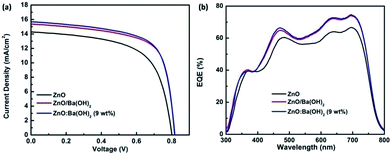 |
| | Fig. 2 (a) J–V characteristics under illumination (AM 1.5 G, one sun) and (b) EQE spectra of devices with ZnO, ZnO/Ba(OH)2 and ZnO:Ba(OH)2 nanocomposite as an ETLs. | |
Table 1 Performance parameters for devices with ZnO, ZnO/Ba(OH)2 and ZnO:Ba(OH)2 nanocomposite as an ETLs
| Electron transport layer (ETL) |
Voc (mV) |
Jsca (mA cm−2) |
FF (%) |
PCEb (%) |
| Jsc as calculated from EQE is shown in parentheses. The average PCE is shown in parentheses. Average PCE was calculated using the results of 5 devices. |
| ZnO |
803 |
14.28 (14.05) |
62.30 |
7.12 (7.07) |
| ZnO/Ba(OH)2 |
814 |
15.34 (15.56) |
68.20 |
8.54 (8.46) |
| ZnO:Ba(OH)2 (9 wt%) |
818 |
15.69 (15.70) |
67.60 |
8.66 (8.59) |
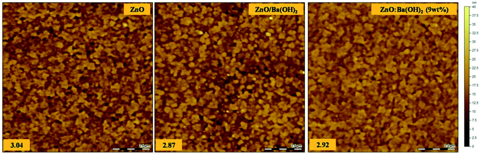
From the previous studies, it is well understood that better hydrophobic properties of ETLs are essential for the intimate contact with the deposited photoactive layer which is spin-coated from dispersion in an organic solvent.41,42 Thus, contact angle measurements were carried out with water drop as the probe for the surface of ZnO, ZnO/Ba(OH)2 and ZnO:Ba(OH)2 (9 wt%) nanocomposite and subsequent values are shown in Table 2 and for all the all the films studies, contact angle values are summarized in Table S2.† From both these tables, two observations were made: (1) it can be seen that in both cases i.e. ZnO/Ba(OH)2 and for all the composition of ZnO:Ba(OH)2 nanocomposite, contact angle is more than ZnO (2) it is observed that contact angle increases with the increase in the wt% of Ba(OH)2 in ZnO:Ba(OH)2 nanocomposite and saturates at around ∼52° for all the compositions after 6 wt%. From both these observations, it is confirmed that films of ZnO/Ba(OH)2 and ZnO:Ba(OH)2 nanocomposite are somewhat more hydrophobic than that of ZnO. But this small increment in contact angle for the films of ZnO/Ba(OH)2 and ZnO:Ba(OH)2 nanocomposite could not be the only reason for the improved PCE and therefore role of morphology and surface topography of ETL is investigated thereafter. It has been well known that the interfacial morphology and surface topography of ETL plays a crucial role and can significantly influence the device performance.43,44 Surface morphology and RMS surface roughness of ZnO, ZnO/Ba(OH)2 and ZnO:Ba(OH)2 (9 wt%) nanocomposite thin films deposited on ITO coated glass substrates are shown in the Fig. 3. It was observed that although the morphology of all the three films are quite similar but RMS surface roughness of the ZnO/Ba(OH)2 and ZnO:Ba(OH)2 (9 wt%) nanocomposite thin films are slightly less as compared to the ZnO. Thus, we believe that smooth surface of these film facilitates with slightly higher contact angle might be facilitating uniform, conformal and intimate contact with the PTB7-Th:PCBM photoactive layer therefore devices with ZnO/Ba(OH)2 and ZnO:Ba(OH)2 (9 wt%) nanocomposite thin films as an ETL performs better than devices with only ZnO as an ETL.
Table 2 Contact angle of the surface of films of ZnO, ZnO/Ba(OH)2 and ZnO:Ba(OH)2 nanocomposite thin films deposited on ITO coated glass substrates
| Electron transport layer (ETL) |
Contact angle (in deg) |
| ZnO |
46.88 ± 0.65 |
| ZnO/Ba(OH)2 |
49.59 ± 0.54 |
| ZnO:Ba(OH)2 (9 wt%) |
52.65 ± 0.81 |
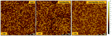 |
| | Fig. 3 Atomic Force Microscopy (AFM) images of ZnO, ZnO/Ba(OH)2 and ZnO:Ba(OH)2 (9 wt%) nanocomposite thin films deposited on ITO coated glass substrates. | |
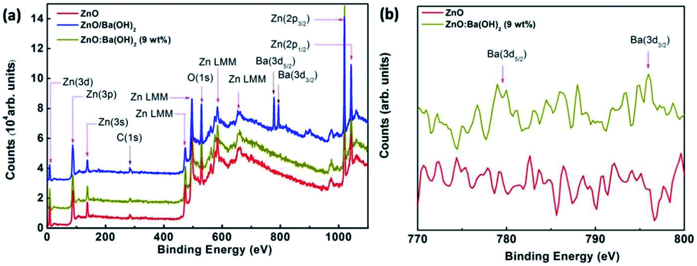
To confirm and demonstrate the presence of Ba in ZnO/Ba(OH)2 and ZnO:Ba(OH)2 (9 wt%) nanocomposite, XPS survey spectra of ZnO, ZnO/Ba(OH)2 and ZnO:Ba(OH)2 (9 wt%) nanocomposite acquired in the range of 0–1170 eV have been taken and are illustrated in Fig. 4(a). During photoemission studies, specimen charging was observed which was later calibrated by assigning the C 1s signal at 284.6 eV. To get the clean surface Ar ion sputtering performed on all three samples for 20 min with average base pressure maintained 6 × 10⁻⁸ torr. Survey spectra of Fig. 4(a) show sharp peaks of C 1s (284.6 eV), O 1s (531 eV) along with the expected peaks of Zn and Ba. Auger peak for Zn (LMM) was also observed. For ZnO, ZnO/Ba(OH)2 and ZnO:Ba(OH)2 (9 wt%) nanocomposite, two prominent peaks at ∼1021.75 eV and ∼1044.25 eV can be attributed to Zn (2p3/2) & Zn (2p1/2), which confirms the presence of ZnO phase formation.23 Also, for ZnO/Ba(OH)2, two prominent peaks at ∼781 eV and ∼796 eV can be attributed to Ba (3d5/2) & Zn (3d3/2).45 However, the intensity of these peaks decreases significantly in the case of ZnO:Ba(OH)2 (9 wt%) nanocomposite and these peaks are absent in the case of ZnO as can be seen in the Fig. 4(b). Thus, it is confirmed that Ba exist in both ZnO/Ba(OH)2 and ZnO:Ba(OH)2 (9 wt%) nanocomposite.
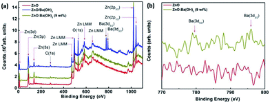 |
| | Fig. 4 (a) XPS Survey scan spectra of ZnO, ZnO/Ba(OH)2 and ZnO:Ba(OH)2 (9 wt%) nanocomposite thin films deposited on ITO coated glass substrates. (b) XPS core level spectra of ZnO and ZnO:Ba(OH)2 (9 wt%) nanocomposite. | |
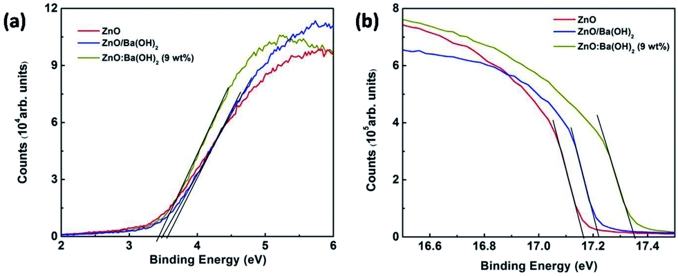
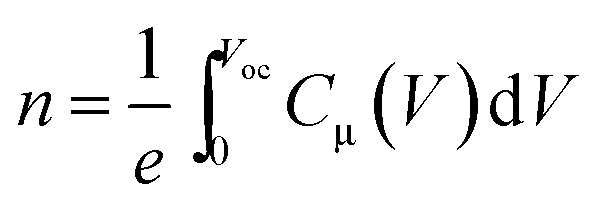
As discussed in the previous section of this paper, the increase in the PCE for devices with ZnO/Ba(OH)2 and ZnO:Ba(OH)2 nanocomposite as an ETL is mainly due to increase in the Jsc and FF. It is well known from the previous studies that Jsc depends on the photon absorption which is material property of donor polymer and both Jsc and FF depends on intrinsic mobility of donor and acceptor, morphology of photoactive and buffer layers and energy level of buffer layers used.46 In the present study, photon absorption, intrinsic mobility of donor and acceptor, morphology of photoactive layer must be same for the three devices as same photoactive layer comprised of PTB7-Th:PCBM has been employed. Further, as discussed in the previous section, there is a slight difference in the morphology, surface roughness and hydrophobic properties of films of ZnO, ZnO/Ba(OH)2 and ZnO:Ba(OH)2 nanocomposite. Thus, it is presumed that there must be the change in the energy levels of these films which is responsible for the increase in the PCE of devices with ZnO/Ba(OH)2 and ZnO:Ba(OH)2 nanocomposite as an ETL. To verify this presumption, UPS measurements are carried out to study the surface electronic energy levels ZnO, ZnO/Ba(OH)2 and ZnO:Ba(OH)2 (9 wt%) nanocomposite thin films and results are shown in Fig. 5(a) and (b). The HOMO level of ZnO, ZnO/Ba(OH)2 and ZnO:Ba(OH)2 (9 wt%) nanocomposite thin films are found to be 7.58, 7.52 and 7.28 eV respectively. This trend is similar to the trend reported for previously reported different ZnO based nanocomposite.34 Thus, it is clear that HOMO level of the ZnO/Ba(OH)2 and ZnO:Ba(OH)2 nanocomposite thin films are lower than that of ZnO (Table 3). The HOMO level was determined by the eqn (1) mentioned in the previous studies:20,47
| | |
HOMO level = hν − (E1 − E2)
| (1) |
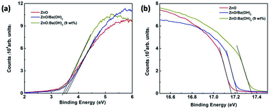 |
| | Fig. 5 UPS spectra of ZnO, ZnO/Ba(OH)2 and ZnO:Ba(OH)2 (9 wt%) nanocomposite thin films deposited on ITO coated glass substrates (a) valence band region (b) cut-off region. | |
Table 3 Various energy levels of ZnO, ZnO/Ba(OH)2 and ZnO:Ba(OH)2 (9 wt%) nanocomposite thin films deposited on ITO coated glass substratesa
| Electron transport layer (ETL) |
E1 |
E2 |
ΔE |
HOMO |
Eg |
LUMO |
| E1 is upper emission onset energies and E2 is the lower emission onset energies. |
| ZnO |
17.16 |
3.53 |
13.63 |
7.58 |
3.22 |
4.36 |
| ZnO/Ba(OH)2 |
17.22 |
3.53 |
13.66 |
7.52 |
3.29 |
4.23 |
| ZnO:Ba(OH)2 (9 wt%) |
17.36 |
3.43 |
13.93 |
7.28 |
3.34 |
3.94 |
Here, hν is incident photon energy (21.2 eV) of He I, and values of E1 and E2 are for ZnO, ZnO/Ba(OH)2 and ZnO:Ba(OH)2 (9 wt%) nanocomposite thin films are shown in Table 3.33,47 The E1 was determined by linear extrapolation to zero at the yield of secondary electrons, and the E2 is the onset relative to the Fermi level (Ef) of Au (0 eV), where the Ef is determined from the Au substrate.47 The LUMO level of ZnO, ZnO/Ba(OH)2 and ZnO:Ba(OH)2 (9 wt%) nanocomposite thin films is determined by using eqn (2) mentioned in the previous studies:47
| | |
LUMO = HOMO − optical band gap,
| (2) |
The LUMO levels of ZnO, ZnO/Ba(OH)2 and ZnO:Ba(OH)2 (9 wt%) nanocomposite thin films are found to be 4.36, 4.26 and 3.94 eV respectively. Thus, it is evident that the LUMO of the ZnO/Ba(OH)2 and ZnO:Ba(OH)2 (9 wt%) nanocomposite thin films is smaller than that of ZnO. This trend is expected and can be explained based on the mechanism reported in the previous studies in which they have discussed the formation of a low work function Zn–O–Ba complex.26,48 Their study suggests that a thin layer of O–Ba is formed on the ZnO surface with Ba ions pointing upwards. Further, the formation of O–Ba replaces the hydroxyl group on the ZnO surface by surface chemical reaction: −OH + Ba+ → O–Ba + H+, a phenomenon similar to chemisorption of Cl-terminated molecules onto ITO. The interface dipoles with a negative charge toward ZnO and the corresponding positive charge toward the upward direction result in the lowering of the vacuum level of ZnO and this might be facilitating the charge transport from PCBM to ETLs.21,48 Further, variation in conductivities of the ETLs are given in Fig. S1b of ESI† and device performance of various devices was compared with the intensity dependent photo-EIS measurements and has been discussed in the subsequent section.
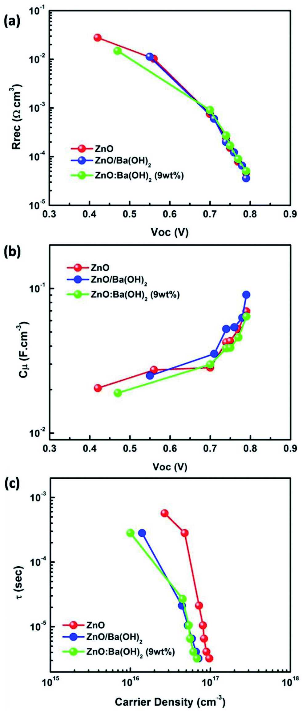
Fig. S3† illustrates Nyquist plot (both raw and fitted) of PTB7-Th:PCBM OSCs with ZnO, ZnO/Ba(OH)2 and ZnO:Ba(OH)2 nanocomposite as ETLs under different illumination intensity. It can be clearly seen that for all the three ETLs, photo-EIS spectra as shown in the Fig. S3(a–c)† consist of only one semi-circle. This is in agreement with the previous reports of PTB7-Th:PCBM OSC and can be explained on the basis of molecular packaging of donor polymer.49,50 In the case of PTB7-Th, like other low bandgap donor polymers, it is a face-on orientation making the inter-electrode transport proceeds through the π–π stacking. As a result, the second semicircle which is generally observed in P3HT:PCBM OSC and corresponds to the charge transport is absent.6,8,9 Therefore, Nyquist plot for PTB7-Th:PCBM OSC can be fitted by a simple circuit shown in the Fig. S4† which consists of a recombination resistance (Rrec) and the chemical capacitance (Cμ) along with the series resistance due to contact and wires (Rs). The obtained values of resistance and the capacitance after fitting were plotted as a function of Voc and have been shown in the Fig. 6(a) and (b) respectively. A critical investigation of these curves approves an exponential decrease and increase of resistance and capacitance respectively with the increase in Voc. Thus, it can be concluded that they represents a bulk and interfacial recombination resistance and chemical capacitance.40,51 A meaningful analysis of charge recombination processes within the device can be obtained by fitting the recombination resistance and chemical capacitance as a function of Voc using the exponential laws mentioned in the eqn (3) and (4).52 The obtained values of α and β can be seen the Table S3.† Further, the response time representative of the recombination processes is calculated from the characteristic frequency (ω) at the top of the arc, where 2πω = 1/τ.53 For all the devices with different ETLs, effective recombination times (τ) range in the order of 10−4 to 10−6 s. Additionally, as discussed in previous studies, it is feasible to estimate the charger carrier density (n) from the chemical capacitance (Cμ) using eqn (5).52
| | |
Rrec ∝ exp(−βVoc/κBT)
| (3) |
| |
 | (5) |
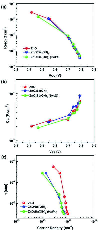 |
| | Fig. 6 (a) Recombination resistance (Rrec) as a function of Voc (b) chemical capacitance (Cμ) as a function of Voc (c) carrier lifetime as a function of the photo-generated carrier density for PTB7-Th:PCBM OSCs with ZnO, ZnO/Ba(OH)2 and ZnO:Ba(OH)2 nanocomposite as an ETLs. | |
Fig. 6(c) illustrates the carrier lifetime as a function of the photo-generated carrier density. All the curves show decay dynamics that follow a power law trend mentioned in the eqn (6).51 The obtained value of λ for PTB7-Th:PCBM OSCs with ZnO, ZnO/Ba(OH)2 and ZnO:Ba(OH)2 nanocomposite as ETLs are shown in the Table S3.† It is necessary to mention here that the impedance measurements allow to establish a direct relation between the exponents of the capacitance and resistance dependences on Voc, and the power-law exponent of τ(n) function as mentioned in the eqn (7).51,52 The obtained values of λ using the eqn (7) for PTB7-Th:PCBM OSCs with ZnO, ZnO/Ba(OH)2 and ZnO:Ba(OH)2 nanocomposite as ETLs are also shown in the Table S3.†
| |
 | (7) |
It can be clearly observed that values of λ as obtained from eqn (6) and (7) for the PTB7-Th:PCBM OSCs with ZnO/Ba(OH)2 and ZnO:Ba(OH)2 nanocomposite as ETLs are in close agreement suggesting that order of recombination (1 + λ) depends not only on the features of the density of states but also on the flux of carrier loss through the parameter β. However, the values of λ as obtained from eqn (6) and (7) for the PTB7-Th:PCBM OSCs with ZnO as ETL are different. In this case, the similar value of λ (as calculated using eqn (7)) can be obtained by using the relation λ = 1/α thereby confirming that order of the recombination exclusively depends on the energy distribution of the trapped states.52,54 This is because the above analyses recognize the recombination as a multiple trapping mechanism in which trapped holes can either recombine with electrons at the acceptor levels or be retrapped at an exponential tail of donor states.52,54 Thus, photo-EIS measurements confirms that PTB7-Th:PCBM OSCs with ZnO/Ba(OH)2 and ZnO:Ba(OH)2 nanocomposite as ETLs performs better than that of PTB7-Th:PCBM OSCs with ZnO as an ETL because the presence of Ba(OH)2 restricts the multiple trapping and minimizes the recombination which was otherwise observed in devices with only ZnO as an ETL.52
4. Conclusion
In conclusion, we have compared the device performance of PTB7-Th:PCBM OSCs in an inverted geometry with ZnO, ZnO/Ba(OH)2 and ZnO:Ba(OH)2 nanocomposite as an ETLs. Our study confirms that devices with ZnO/Ba(OH)2 and ZnO:Ba(OH)2 nanocomposite as ETL demonstrates improved performance parameters compared to devices with only ZnO as ETL. It is observed that films of ZnO/Ba(OH)2 and ZnO:Ba(OH)2 nanocomposite have low work function and are slightly more smooth and hydrophobic as compared to ZnO films. This might have suppressed the charge recombination and thereby improved the charge collection as has been confirmed by EIS measurements.
Conflicts of interest
There are no conflicts to declare.
Acknowledgements
The authors would like to acknowledge the support of Center of Excellence in Nanoelectronics (CEN), National Center for Photovoltaic Research and Education (NCPRE), Department of Metallurgical Engineering and Materials Science (MEMS) and Sophisticated Analytical Instrument Facility (SAIF) at Indian Institute of Technology Bombay (IIT Bombay) Mumbai for providing various facilities for device fabrication and characterization. A. Y. thanks the DST-INSPIRE fellowship for the financial support. We also thank for partial support under the Solar Energy Research Institute for India and the United States (SERIIUS), funded jointly by the U.S. Department of Energy (Office of Science, Office of Basic Energy Sciences, and Energy Efficiency and Renewable Energy, Solar Energy Technology Program, under Subcontract DE-AC36-08GO28308 to the National Renewable Energy Laboratory, Golden, Colorado) and the Government of India, through the Department of Science and Technology under Subcontract IUSSTF/JCERDC-SERIIUS/2012 dated 22nd Nov. 2012.
References
- G. Yu, J. Gao, J. C. Hummelen, F. Wudl and A. J. Heeger, Science, 1995, 270, 1789–1791 CAS
 .
. - Z. C. He, C. M. Zhong, S. J. Su, M. Xu, H. B. Wu and Y. Cao, Nat. Photonics, 2012, 6, 591–595 CrossRef .
- W. C. Huang, N. Chandrasekaran, S. K. K. Prasad, E. Gann, L. Thomsen, D. Kabra, J. M. Hodgkiss, Y. B. Cheng and C. R. McNeill, ACS Appl. Mater. Interfaces, 2016, 8, 29608–29618 CAS .
- N. Chandrasekaran, E. Gann, N. Jain, A. Kumar, S. Gopinathan, A. Sadhanala, R. H. Friend, A. Kumar, C. R. McNeill and D. Kabra, ACS Appl. Mater. Interfaces, 2016, 8, 20243–20250 CAS .
- N. S. Sariciftci, L. Smilowitz, A. J. Heeger and F. Wudl, Science, 1992, 258, 1474–1476 CAS .
- S. R. Gollu, R. Sharma, G. Srinivas, S. Kundu and D. Gupta, Org. Electron., 2014, 15, 2518–2525 CrossRef CAS .
- R. Sharma, S. Bhalerao and D. Gupta, Org. Electron., 2016, 33, 274–280 CrossRef CAS .
- S. R. Gollu, R. Sharma, G. Srinivas, S. Kundu and D. Gupta, Org. Electron., 2015, 24, 43–50 CrossRef CAS .
- S. R. Gollu, R. Sharma, G. Srinivas, S. Kundu and D. Gupta, Org. Electron., 2016, 29, 79–87 CrossRef CAS .
- G. Dennler, R. Gaudiana and C. J. Brabec, Abstr. Pap. Am. Chem. Soc., 2009, 238 Search PubMed .
- T. Ameri, P. Khoram, J. Min and C. J. Brabec, Adv. Mater., 2013, 25, 4245–4266 CrossRef CAS PubMed .
- L. Y. Lu, T. Y. Zheng, Q. H. Wu, A. M. Schneider, D. L. Zhao and L. P. Yu, Chem. Rev., 2015, 115, 12666–12731 CrossRef CAS PubMed .
- B. Walker, H. Choi and J. Y. Kim, Curr. Appl. Phys., 2017, 17, 370–391 CrossRef .
- Z. G. Yin, J. J. Wei and Q. D. Zheng, Adv. Sci., 2016, 3, 1–37 Search PubMed .
- W. C. H. Choy and D. Zhang, Small, 2016, 12, 416–431 CrossRef CAS PubMed .
- H. Zeng, X. C. Zhu, Y. Y. Liang and X. G. Guo, Polymers (Basel), 2015, 7, 333–372 CrossRef CAS .
- Z. C. Hu, K. Zhang, F. Huang and Y. Cao, Chem. Commun., 2015, 51, 5572–5585 RSC .
- V. Gupta, A. K. K. Kyaw, D. H. Wang, S. Chand, G. C. Bazan and A. J. Heeger, Sci. Rep. UK, 2013, 3, 1–6 Search PubMed .
- S. Woo, W. H. Kim, H. Kim, Y. Yi, H. K. Lyu and Y. Kim, Adv. Energy Mater., 2014, 4, 1–7 Search PubMed .
- A. K. K. Kyaw, D. H. Wang, V. Gupta, J. Zhang, S. Chand, G. C. Bazan and A. J. Heeger, Adv. Mater., 2013, 25, 2397–2402 CrossRef CAS PubMed .
- Z. A. Tan, S. S. Li, F. Z. Wang, D. P. Qian, J. Lin, J. H. Hou and Y. F. Li, Sci. Rep. UK, 2014, 4, 1–9 Search PubMed .
- S. Kundu, S. R. Gollu, R. Sharma, G. Srinivas, A. Ashok, A. R. Kulkarni and D. Gupta, Org. Electron., 2013, 14, 3083–3088 CrossRef CAS .
- R. Sharma, H. Lee, K. Borse, V. Gupta, A. G. Joshi, S. Yoo and D. Gupta, Org. Electron., 2017, 43, 207–213 CrossRef CAS .
- S. K. Hau, H. L. Yip, N. S. Baek, J. Y. Zou, K. O'Malley and A. K. Y. Jen, Appl. Phys. Lett., 2008, 92, 253301 CrossRef .
- Z. H. Lin, C. Y. Jiang, C. X. Zhu and J. Zhang, ACS Appl. Mater. Interfaces, 2013, 5, 713–718 CAS .
- H. Zhang, T. Stubhan, N. Li, M. Turbiez, G. J. Matt, T. Ameri and C. J. Brabec, J. Mater. Chem. A, 2014, 2, 18917–18923 CAS .
- S. I. Na, T. S. Kim, S. H. Oh, J. Kim, S. S. Kim and D. Y. Kim, Appl. Phys. Lett., 2010, 97, 253305 CrossRef .
- H. Choi, J. S. Park, E. Jeong, G. H. Kim, B. R. Lee, S. O. Kim, M. H. Song, H. Y. Woo and J. Y. Kim, Adv. Mater., 2011, 23, 2759–2763 CrossRef CAS PubMed .
- Y. X. Zhu, X. F. Xu, L. J. Zhang, J. W. Chen and Y. Cao, Sol. Energy Mater. Sol. Cells, 2012, 97, 83–88 CrossRef CAS .
- L. Yan, Y. X. Song, Y. Zhou, B. Song and Y. F. Li, Org. Electron., 2015, 17, 94–101 CrossRef CAS .
- P. Li, G. Wang, L. Cai, B. F. Ding, D. C. Zhou, Y. Hu, Y. J. Zhang, J. Xiang, K. M. Wan, L. J. Chen, K. Alameh and Q. L. Song, Phys. Chem. Chem. Phys., 2014, 16, 23792–23799 RSC .
- X. Min, F. Y. Jiang, F. Qin, Z. F. Li, J. H. Tong, S. X. Xiong, W. Meng and Y. H. Zhou, ACS Appl. Mater. Interfaces, 2014, 6, 22628–22633 CAS .
- H. C. Chen, S. W. Lin, J. M. Jiang, Y. W. Su and K. H. Wei, ACS Appl. Mater. Interfaces, 2015, 7, 6273–6281 CAS .
- N. Wu, Q. Luo, Z. M. Bao, J. Lin, Y. Q. Li and C. Q. Ma, Sol. Energy Mater. Sol. Cells, 2015, 141, 248–259 CrossRef CAS .
- X. R. Jia, N. Wu, J. F. Wei, L. P. Zhang, Q. Luo, Z. M. Bao, Y. Q. Li, Y. Z. Yang, X. G. Liu and C. Q. Ma, Org. Electron., 2016, 38, 150–157 CrossRef CAS .
- L. P. Lu, D. Kabra and R. H. Friend, Adv. Funct. Mater., 2012, 22, 4165–4171 CrossRef CAS .
- N. K. Kim, D. Khim, Y. Xu, S. H. Lee, M. Kang, J. Kim, A. Facchetti, Y. Y. Noh and D. Y. Kim, ACS Appl. Mater. Interfaces, 2014, 6, 9614–9621 CAS .
- W. C. Zhao, L. Ye, S. Q. Zhang, H. F. Yao, M. L. Sun and J. H. Hou, J. Phys. Chem. C, 2015, 119, 27322–27329 CAS .
- K. Borse, R. Sharma, H. P. Sagar, P. A. Reddy, D. Gupta and A. Yella, Org. Electron., 2017, 41, 280–286 CrossRef CAS .
- R. Sharma, H. Lee, V. Gupta, H. Kim, M. Kumar, C. Sharma, S. Chand, S. Yoo and D. Gupta, Org. Electron., 2016, 34, 111–117 CrossRef CAS .
- S. H. Liao, H. J. Jhuo, Y. S. Cheng and S. A. Chen, Adv. Mater., 2013, 25, 4766–4771 CrossRef CAS PubMed .
- S. H. Liao, H. J. Jhuo, P. N. Yeh, Y. S. Cheng, Y. L. Li, Y. H. Lee, S. Sharma and S. A. Chen, Sci. Rep., 2014, 4, 1–7 Search PubMed .
- J. B. You, C. C. Chen, L. T. Dou, S. Murase, H. S. Duan, S. A. Hawks, T. Xu, H. J. Son, L. P. Yu, G. Li and Y. Yang, Adv. Mater., 2012, 24, 5267–5272 CrossRef CAS PubMed .
- Q. Q. Sun, F. J. Zhang, J. Wang, Q. S. An, C. Zhao, L. L. Li, F. Teng and B. Hu, J. Mater. Chem. A, 2015, 3, 18432–18441 CAS .
- P. Nachimuthu, Y. J. Kim, S. V. N. T. Kuchibhatla, Z. Q. Yu, W. Jiang, M. H. Engelhard, V. Shutthanandan, J. Szanyi and S. Thevuthasan, J. Phys. Chem. C, 2009, 113, 14324–14328 CAS .
- I. Etxebarria, J. Ajuria and R. Pacios, Org. Electron., 2015, 19, 34–60 CrossRef CAS .
- Y. H. Kim, T. H. Han, H. Cho, S. Y. Min, C. L. Lee and T. W. Lee, Adv. Funct. Mater., 2014, 24, 3808–3814 CrossRef CAS .
- J. S. Huang, Z. Xu and Y. Yang, Adv. Funct. Mater., 2007, 17, 1966–1973 CrossRef CAS .
- Q. Wan, X. Guo, Z. Y. Wang, W. B. Li, B. Guo, W. Ma, M. J. Zhang and Y. F. Li, Adv. Funct. Mater., 2016, 26, 6635–6640 CrossRef CAS .
- B. B. Sun, D. Y. Zhou, C. Wang, P. Liu, Y. J. Hao, D. W. Han, L. Feng and Y. Zhou, Org. Electron., 2017, 44, 176–182 CrossRef CAS .
- A. Guerrero, N. F. Montcada, J. Ajuria, I. Etxebarria, R. Pacios, G. Garcia-Belmonte and E. Palomares, J. Mater. Chem. A, 2013, 1, 12345–12354 CAS .
- P. P. Boix, J. Ajuria, R. Pacios and G. Garcia-Belmonte, J. Appl. Phys., 2011, 109, 074514 CrossRef .
- T. M. Clarke, C. Lungenschmied, J. Peet, N. Drolet and A. J. Mozer, Adv. Energy Mater., 2015, 5, 1–11 Search PubMed .
- M. P. Eng, P. R. F. Barnes and J. R. Durrant, J. Phys. Chem. Lett., 2010, 1, 3096–3100 CrossRef CAS .
Footnotes |
| † Electronic supplementary information (ESI) available. See DOI: 10.1039/c7ra13428b |
| ‡ Kunal Borse and Ramakant Sharma contributed equally to this work. |
|
| This journal is © The Royal Society of Chemistry 2018 |
Click here to see how this site uses Cookies. View our privacy policy here. 
 Open Access Article
 This Open Access Article is licensed under a
  *a
*a