DOI:
10.1039/C7RA13289A
(Paper)
RSC Adv., 2018,
8, 11574-11579
Improving the photovoltaic performance of planar heterojunction perovskite solar cells by mixed solvent vapor treatment†
Received
13th December 2017
, Accepted 17th March 2018
First published on 23rd March 2018
Abstract
The grain size of perovskite films is a key factor to optimize the performance of perovskite photovoltaic devices. Herein, a new route is developed in this paper to prepare CH3NH3PbI3 (MAPbI3) films with a better morphology and crystallization. This method includes the spin coating deposition of perovskite films with a precursor solution of PbI2 and CH3NH3I at the molar ratio 1![[thin space (1/6-em)]](https://www.rsc.org/images/entities/char_2009.gif) :1 and thermal annealing (TA). The thermal annealing is conducted with a thermal-induced process to realize grain growth with solvent evaporation. In addition, a mixed solvent vapor treatment in acetic acid with chlorobenzene (HAc/CB) improves the morphology and crystallization of films further. As a result, the photovoltaic device based on the perovskite film treated by mixed HAc/CB solvent exhibits the best efficiency of 13.15% in comparison to the control device with 11.44% under AM 1.5G irradiation (100 mW cm−2).
:1 and thermal annealing (TA). The thermal annealing is conducted with a thermal-induced process to realize grain growth with solvent evaporation. In addition, a mixed solvent vapor treatment in acetic acid with chlorobenzene (HAc/CB) improves the morphology and crystallization of films further. As a result, the photovoltaic device based on the perovskite film treated by mixed HAc/CB solvent exhibits the best efficiency of 13.15% in comparison to the control device with 11.44% under AM 1.5G irradiation (100 mW cm−2).
Introduction
The hybrid organolead halide perovskite solar cells (PSCs) have attracted much attention due to their controlled composition, lower-cost organic components, high charge carrier mobility properties,1,2 extremely low trap-state density,3 lesser exciton binding energy,4 longer charge carrier diffusion length5,6 and excellent absorption coefficient.7 At present, the power conversion efficiencies (PCE) of PSCs has increased rapidly to 22.1% since perovskite solar cells were first reported in 2009.8,9 PSCs have offered a promising route to fabricate solar cells via low-cost manufacturing process compared with traditional thin-film photovoltaic cells such as CIGS solar cells,10 which are the new comers of the third-generation photovoltaic devices. Several typical technique processes to fabricate PSCs have been developed recently, including the solution-processed method,11–13 the vacuum vapor phase deposition14 and other combination thereof.15 Compared with other methods, the solution process has great advantages due to the simple process and the low deposition equipment costs.
Furthermore, the solvent engineering has been proven to be a resultful deposition technology to enhance the grain size and uniform perovskite layers.16–20 Sang II Seok et al. declared that dimethyl sulfoxide (DMSO) served as a cosolvent with the gamma-butyrolactone (GBL) solution dissolving CH3NH3I (MAI) and PbI2 via one-step spin coating method,21 which boot the dissolubility of perovskite precursor and form dense films. Subsequently, they kept meliorating the techniques by a method with direct intramolecular exchange of DMSO molecules intercalated in PbI2 involving formamidinium iodide (FAI) via a sequential two-step coating method.22 Then they further elucidated that DMSO strongly interacts with DMSO and PbI2, and retard crystallization of the perovskite films. As we all known, a few polar organic molecules (e.g. DMSO, DMF) easily were absorbed into the perovskite materials.23,24 The residual solvent in perovskite films dramatically destroy the crystal structure, which accelerated the ion migration and lattice deformation on account of charges accumulation and then weaken the stability of the perovskite layers.25 A long time and high temperature annealing process would remove the residual molecules at the cost of losing counter ions in the surface, which increases the thin film defect and shortens the perovskite device performance.26 Seok et al. applied the toluene drip-casting treatment during the spinning in one-step process.21 Instead of toluene, Nam-Gyu Park et al. account that diethyl ether was a more advisable to remove DMSO and DMF solvent.27 Nevertheless, either annealing process or diethyl ether treatment could not entirely remove the residual DMSO and FAI(MAI)-DMSO species.28 The solar cells would explicitly deteriorate because that the residuary solvent induced the degradation of perovskite layers.29 It is an intractable issue to remove the remnant solvent involved in the preparation process of thin films, especially the solvent still remained in the films after thermal annealing. However, it has not been investigated with respect to the PSCs performance so far for the effect of solvent treatment after thermal annealing of perovskite films.
Here, we investigated the PSCs performance with the solvent vapour treatment after the thermal annealing (TA). The CH3NH3PbI (MAPbI3) film preparing process involved one step deposition through perovskite precursor solution and acetic acid (HAc) with chlorobenzene (CB) mixed solvent vapor treatment process (H/CVT), which could effectively increase the crystallinity and improve the morphology quality. The films prepared based on H/CVT process were characterized by the scanning electron microscope (SEM), the X-ray diffraction (XRD) and time-resolved photoluminescence (PL) decay curves, in comparison with the films with prepared only by one-step thermal annealing (TA) processes. Then the photovoltaic devices were prepared and the dependence of their performance were discussed in the various process conditions. The fabricated photovoltaic devices based H/CVT process exhibited the best PCE up to 13.15% under AM 1.5G radiation (100 mW cm−2) and in comparison to control devices with a 14.9% improvement.
Experimental
Materials
PbI2 and CH3NH3I were purchased from Xi'an Polymer Light Technology Corp. Acetic acid (HAc, purity > 99.99%) and chlorobenzene (CB) were purchased from Sigma-Aldrich. PCBM was purchased from Nano-C. The precursor solution of CH3NH3PbI3 was composed of PbI2 and CH3NH3I with a molar ratio of 1:1 and was stirred in a mixture of dimethyl sulfoxide (DMSO) and γ-butyrolactone (GBL) (3/7, v/v) at 60 °C overnight. Phenyl-C61-butyric acid methyl ester (PCBM) was dissolved in o-dichlorobenzene with a concentration of 20 mg ml−1.
Solar cells fabrication and characterization
All the solar cells were fabricated on indium tin oxide (ITO)-coated glass substrates. The ITO substrates were consecutively cleaned in ultrasonic baths containing glass lotion, de-ionized water, ethanol. The cleaned ITO substrates were then blow-dried by nitrogen gas. All pre-cleaned ITO substrates were treated by UV-ozone cleaner for 10 min to improve work function and then transferred into a nitrogen-filled glove box. The filtered PEDOT:PSS (Clevios, Al4083) was coated on ITO glass substrates by spin-coating at 4000 round per minute (rpm) for 40 s and annealed at 120 °C for 20 min. The perovskite precursor solution was deposited onto ITO/PEDOT:PSS substrates by a consecutive two-step spin-coating process as described in previous reports,21 but using chlorobenzene as an anti-solvent. The as-deposited perovskite films were heat treated with TA and H/CVT process respectively. For the TA process, the perovskite precursor coated substrates were dried onto a hot plate at 100 °C for 5 min. For the H/CVT process the perovskite film heat treated through TA process was continued treating under thermal condition at 70 °C for 3 min in glove-box. For the H/CVT process, the perovskite film were put into Petri dishes (with cover but not sealed) with vapor of mixed solvents of HAc and CB with defined volume ratios (1/50, 1/25, 3/50, v/v). The substrates were treated under thermal condition at 70 °C without touching the mix-solvent. Afterwards, the PCBM layer was then spin-coated onto the CH3NH3PbI3 layer at 1500 rpm for 60 s. Finally, the devices were finished by thermal evaporating Al (80 nm) under 4 × 10⁻⁴ Pa vacuum condition. The device area is defined to be the overlap of the ITO and Al electrodes to be 4 mm2.
The current density–voltage (J–V) curves of the devices were measured with a source meter (Keithley 2400) and measurement unit under simulated AM 1.5G sun spectrum with 100 mW cm−2 irradiation generated by an ABET Sun 2000 solar simulator in air. External quantum efficiency (EQE) was measured by Zolix Solar Cell Scan 100. Ultraviolet-visible absorption spectra were tested on a Shimadzu UV-3101PC spectrophotometer in the 400–800 nm wavelength range at room temperature. All characterizations were done outside the glovebox and without any encapsulation of the perovskite cells, under constant exposure to ambient atmosphere. Steady-state photoluminescence (PL) spectra were recorded by Horiba FluoroLog Spectrophotometer. PL measurements of the perovskite films were covered with a polymethyl methacrylate (PMMA) layer to prevent degradation from ambient atmosphere. Scanning electron microscope (SEM) measurements were performed using a Hitachi, S-4800 SEM equipped with the energy dispersive X-ray spectrum. X-ray diffraction (XRD) spectra was performed on a D/max 2200v X-ray powder diffractometer equipped with Cu-Kα radiation (λ = 1.540 Å), the data were collected at room temperature in the range of 10–50°.
Results and discussion
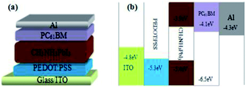
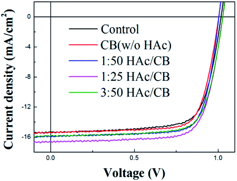
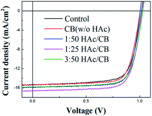
Fig. 1 illustrates the preparation procedure of the CH3NH3PbI3 (MAPbI3) perovskite films in our research. The pristine perovskite films firstly were prepared based on the study of Seo et al.,17 in which non-polar solvent chlorobenzene (CB) was dripped onto the substrates surface during spinning. Afterwards, the substrates were transferred onto the heated platform, the perovskite films turn into dark brown quickly. For the H/CVT process, the perovskite films were subjected to the post-heating treatment, then the perovskite films were put into a Petri dish with the vapor of mixed solvents of HAc and CB. 15 μL mixed solvent was dripped into the Petri dish edge, the as-samples were covered by a glass Petri dish rapidly (with cover but not sealed). The perovskite films were annealed by the mixed solvent of HAc/CB with various volume ratios of HAc (1/50, 1/25, 3/50, v/v). The architecture of the p-i-n PSC with ITO/PEDOT:PSS/MAPbI3/[6,6]-phenyl-C61-butyric acid methyl ester (PCBM)/Al is schematically shown in Fig. 2(a) and the corresponding energy levels of each layer are shown in Fig. 2(b). The control device with the same structure was also fabricated for the comparation without HAc/CB mixing vapor treatment. The J–V characteristic curves of the PSCs of various process conditions are shown in Fig. 3. In addition, the average values of the device parameters obtained from 8 PSCs in each experimental group, which are extracted from the J–V curves are listed in Table 1. According to the photovoltaic performance (Fig. 3 and Table 1), the vapor treatment level for the highest PCE is 1/25 volume ratio of HAc. In order to further investigate the mechanism of the enhanced performance of PSCs with HAc thermal treatment, the superior mixing ratio of 1/25 volume ratio is used in this study. The control group without using HAc/CB mixing vapor treatment has a PCE of 11.44%, which is similar to the values obtained in previous studies for this structure.18,30,31 The maximum improvement in PCE is obtained when 1/25 volume ratio mixed HAc/CB solvent was used. In this case, the median PCE value increases from 11.44% to 13.15%, corresponding to a 14.9% improvement. This improvement in PCE is primarily due to the 7.1% enhancement of Jsc, which increases from 15.38 to 16.47 mA cm−2, as shown in Fig. 3 and Table 1. To be fair, our champion control device is 12.05%, which reveals that our control cells show performance comparable to the results reported in Table 2.17,32–36
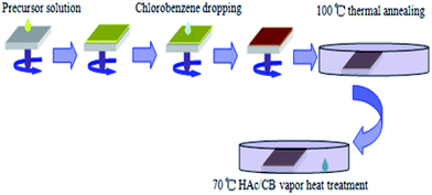 |
| | Fig. 1 Schematic diagram of the thermal treatment of perovskite films under solvent vapor. | |
 |
| | Fig. 2 (a) Schematic device architecture of the p-i-n PSCs constructed by ITO/PEDOT:PSS/CH3NH3PbI3/PCBM/Al; (b) schematic energy band diagram of perovskite solar cells. | |
 |
| | Fig. 3 J–V characteristics of MAPbI3 devices with HAc mixing different volume ratios under 100 mW cm−2 (AM 1.5G). | |
Table 1 Photovoltaic parameters of devices by thermal treatment of the mixed HAc/CB solvent with different volume ratios conditions. Average PCE values were based on 8 devices of each type
| Treatment type |
Jsc (mA cm−2) |
Voc (V) |
FF (%) |
PCEaverage (%) |
PCEbest (%) |
| Control |
15.38 |
1.02 |
73 |
11.44 ± 0.52 |
12.05 |
| With CB (w/o HAc) |
15.46 |
1.01 |
75 |
11.64 ± 0.42 |
12.17 |
| 1:50 HAc with CB |
16.13 |
1.01 |
75 |
12.41 ± 0.31 |
12.88 |
| 1:25 HAc with CB |
16.47 |
1.03 |
75 |
12.80 ± 0.30 |
13.15 |
| 3:50 HAc with CB |
15.93 |
1.03 |
75 |
12.24 ± 0.30 |
12.61 |
Table 2 Photovoltaic performance of perovskite solar cells with device architecture of ITO/PEDOT:PSS/CH3NH3PbI3/PCBM/Al in some reported works
| Jsc (mA cm−2) |
Voc (V) |
FF (%) |
PCEaverage (%) |
PCEbest (%) |
Ref. |
| 16.62 |
0.92 |
80 |
11.80 |
12.20 |
17 |
| 18.02 |
0.85 |
75 |
11.43 |
— |
32 |
| 19.12 |
0.87 |
73 |
11.62 |
12.13 |
33 |
| 18.6 |
0.92 |
72 |
— |
12.30 |
34 |
| 19.2 |
0.85 |
71 |
11.50 |
— |
35 |
| 16.12 |
1.05 |
67 |
— |
12.04 |
36 |
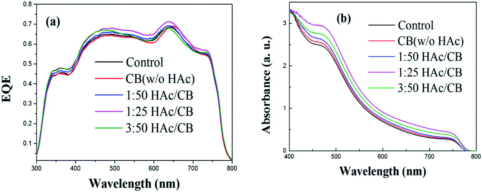
To investigate the main reason responsible for the improvement of Jsc, we conduct external quantum efficiency (EQE) measurements to account for the contribution of photocurrent collection to the incoming photon energy. The EQE spectra illustrates a substantial improvement across the visible region when the H/CVT process applied as shown in Fig. 4(a). We ascribe the enhancement at the 400 to 800 nm to the stronger absorption of the MAPbI3 film shown in Fig. 4(b). The H/CVT films demonstrate a strong absorption in the range between 400 and 780 nm with an onset absorption at 800 nm, which corresponds to a bandgap of 1.55 eV. The more intense absorption of the films with the acetic acid vapor thermal treatment should also be partially attributed to the more homogenous morphology, which are supported by SEM images of the films discussed later. The EQE measurement of two PSCs follows the same trend of the UV-vis absorption spectra.37 The EQE is product of light harvesting efficiency, charge injection/transfer efficiency, and charge collection efficiency. The light harvesting efficiency is higher in the experimental condition of H/CVT films than the control device, indicating that H/CVT will contribute to the higher photo-to-electron conversion efficiency. The improvement of film quality is favourable to the charge transport and the light absorption, than the highest Jsc of the 1/25 volume ratios H/CVT device was achieved. Each device shows almost same values of Voc, which is plausible as Voc determined by the difference between the electron quasi-Fermi level of n-type semiconductor (PCBM in our device) and hole quasi-Fermi level of p-type semiconductor (PEDOT:PSS in our device).38
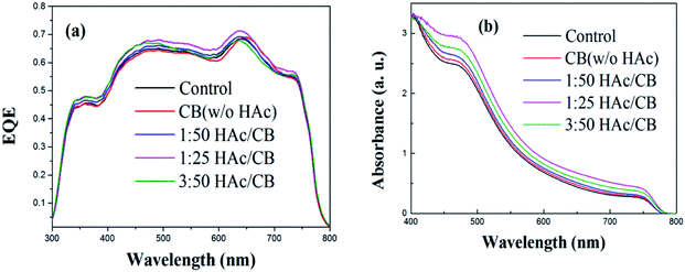 |
| | Fig. 4 (a) EQE spectra of devices treated without and with different volume ratios HAc/CB (b) UV-vis absorption spectra of MAPbI3 film were treated without and with various volume ratios HAc/CB. | |
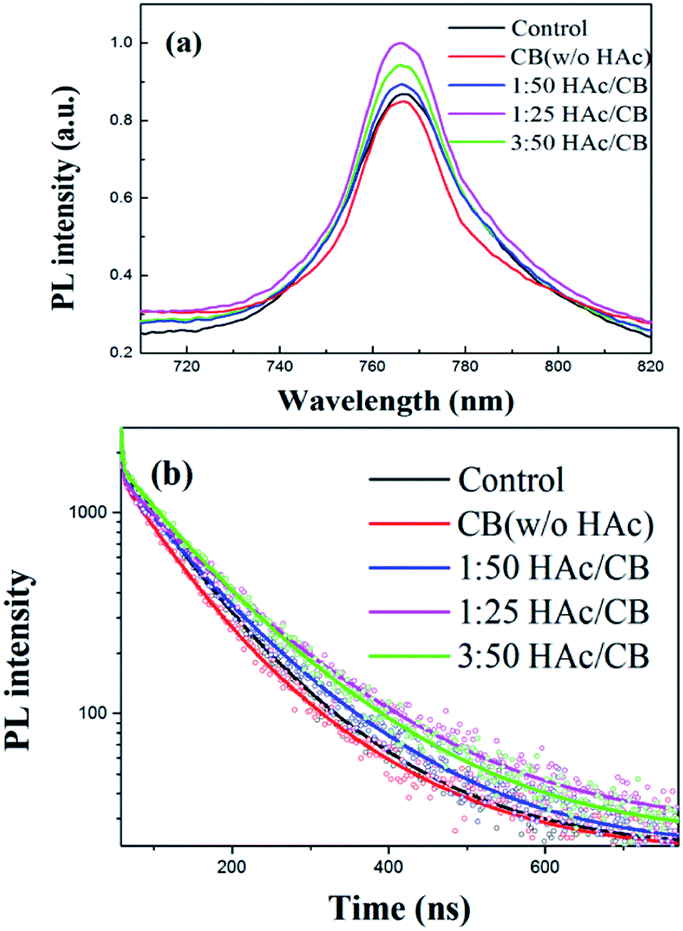
An excitation light of 505 nm falls on the glass/MAPbI3 film without and with various volume ratio HAc/CB mixing vapor treatment from the air side, and the photoluminescence (PL) signal was also collected from the air side to compared the film quality. All samples exhibit a PL peak at 766 nm in Fig. 5(a), which is in agreement with the data reported elsewhere.32,39 Generally, the photoluminescence emission is related to the charge carrier recombination of the bandgap and trap states. The phenomenon may imply the perovskite thin film under H/CVT process has a lower trap density around the band-edge than the control film due to the relative high intensity of PL, which is expected to reduce the recombination loss and improve the photocurrent collection. Meanwhile, we measured the time-resolved PL decay curves of a glass/MAPbI3 film without and with various volume ratio HAc/CB mixing vapor treatment as shown in Fig. 5(b). From the deconvolution of the time-resolved PL decays with a tri-exponential function, the average PL lifetime of 1/25 volume ratios H/CVT film(∼118.25 ns) is longer than that of control film (∼93.12 ns) as listed in Table 3, which is comparable to the value found in MAPbI3 film in previous reports.39 The faster PL quenching in the control film than in the H/CVT film confirms that the recombination loss of the charge carriers in the control film is more than that of H/CVT film. It indicates the improved H/CVT film suppresses the nonradiative recombination channels.
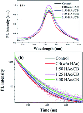 |
| | Fig. 5 (a) Steady-state photoluminescence spectra of MAPbI3 film coated on glass substrate; (b) time-resolved photoluminescent decay curves of glass/MAPbI3 film were treated without and with various volume ratios HAc/CB. | |
Table 3 Time resolved photoluminescence decay characterization
| Treatment type |
τ1 (ns) |
Fraction 1 |
τ2 (ns) |
Fraction 2 |
τ3 (ns) |
Fraction 3 |
Average (ns) |
| Control |
1.00 |
3.34% |
65.92 |
55.64% |
137.52 |
41.02% |
93.12 |
| With CB (w/oHAc) |
1.05 |
4.45% |
60.88 |
50.79% |
139.19 |
44.76% |
93.26 |
| 1:50 HAc with CB |
1.06 |
3.60% |
67.39 |
40.82% |
137.22 |
55.58% |
103.81 |
| 1:25 HAc with CB |
1.06 |
3.12% |
67.81 |
26.91% |
142.97 |
69.93% |
118.25 |
| 3:50 HAc with CB |
0.97 |
2.87% |
71.50 |
40.92% |
143.38 |
56.21% |
109.88 |
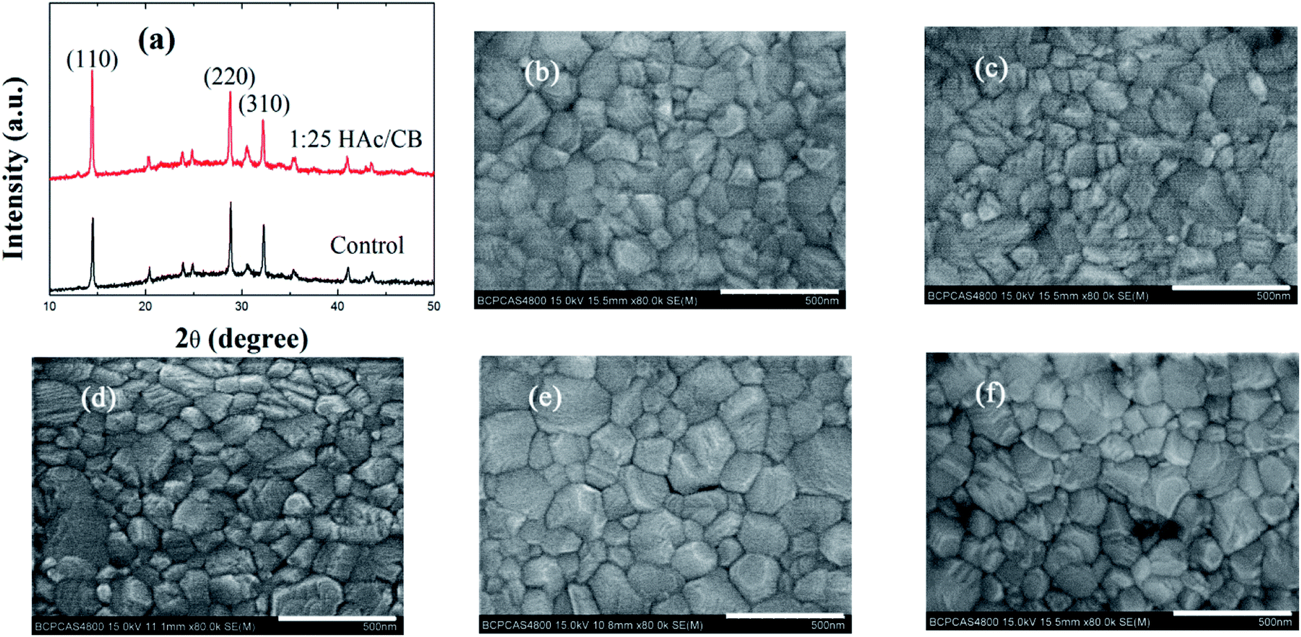
The variation of the carrier recombination in PSCs also correlates with the crystallization property of the perovskite thin films. Hence, the scanning electron microscope (SEM) images and X-ray diffraction (XRD) spectroscopy of MAPbI3 thin films without and with H/CVT process were measured. The crystallization of the MAPbI3 film is a crucial parameter, which is correlated to the light-absorption ability, charge transport and recombination properties of PSCs. The large grain size and good crystallinity will lead to a high performance of the resulting devices.40 Fig. 6(a) shows the X-ray diffraction (XRD) spectroscopy of the MAPbI3 film treated by 1/25 volume ratio HAc/CB mixing solvent and without, respectively. With the similar film thickness and under the same measurement condition, the diffraction peak intensity (110) of the MAPbI3 film processed with HAc vapor treatment is higher than that of the MAPbI3 film without HAc treatment. In general, XRD peak intensity is related to the crystal orientation and surface porosity. The XRD spectra present intense diffraction peaks at 14.50°, 28.84°, and 32.28° in two samples, corresponding to (110), (220), and (310) crystal planes of MAPbI3,41 respectively. SEM images shown in Fig. 6(b)–(f) reveal an interesting phenomena that the grain size of the perovskite film with HAc/CB mixed solvent treatment is larger than that only annealing processes. Extremely the MAPbI3 film of 1/25 volume ratios HAc/CB mixing solution shows a larger grain, which is comparable to other treated films. The average MAPbI3 grain size of the film treated with 1/25 H/CVT and only TA is circa 160 nm and 130 nm, respectively. Using nano measurer software, we assess the maximum grain size of MAPbI3 film treated with 1/25 H/CVT and only TA is 360 nm and 310 nm, respectively. The enlargement of the perovskite grain size reveals fewer grain boundaries which correlate to a lower trap density.2,35,39,42,43 As the recombination in PSCs is evidenced to be governed by the trap states,44 the larger grain size of the perovskite film with HAc/CB mixed solvent vapor treatment indicates less recombination. Hence, we can conclude that the large grain size of the perovskite thin films with HAc/CB mixed solvent treatment contribute to decrease the charge carrier recombination. This result is in accordance with the XRD patterns, and reveales that with HAc/CB mixed solvent treatment perovskite thin films are favor to the growth of large grain MAPbI3 films.
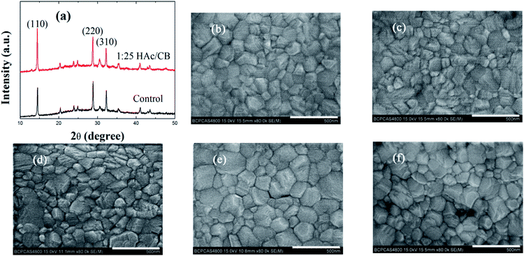 |
| | Fig. 6 (a) XRD patterns of MAPbI3 films were treated without and with 1/25 volume ratios HAc/CB, respectively; (c) SEM image of the MAPbI3 film prepared with CB vapor treatment; (b), (d), (e) and (f) SEM images of MAPbI3 films prepared without and with 1/50, 1/25, 3/50 volume ratios HAc/CB, respectively, scale bar is 500 nm. | |
Conclusions
In summary, we have demonstrated a route to treat MAPbI3 perovskite layers by mixed solvents with HAc and CB, which improves the photoelectric characteristic of the corresponding PSCs, and significantly boosts the devices efficiency (≈15%). The PSCs treated by 1/25 volume ratios H/CVT show a greater photocurrent and less charge carries non-radioactive recombination. We attribute the enhancements to the improved light absorption and the larger grain size that helps to reduce carries losses. This work provides the significant development potential of solvent vapor treatment process after the thermal annealing of perovskite thin films, which emphasizes an effective strategy to facilitate the efficient device performance of the planar heterojunction PSCs toward practical applications in the future.
Conflicts of interest
There are no conflicts to declare.
Acknowledgements
The authors express the thanks to the National Natural Science Foundation of China under Grant No. 61575019 and the Fundamental Research Funds for the Central Universities with the Grant No. 2017RC015.
References
- C. Wehrenfennig, M. Liu, H. J. Snaith, M. B. Johnston and L. M. Herz, Energy Environ. Sci., 2014, 7, 2269–2275 CAS.
- Z. Xiao, Q. Dong, C. Bi, Y. Shao, Y. Yuan and J. Huang, Adv. Mater., 2014, 26, 6503–6509 CrossRef CAS PubMed.
- D. Shi, V. Adinolfi, R. Comin, M. Yuan, E. Alarousu, A. Buin, Y. Chen, S. Hoogland, A. Rothenberger and K. Katsiev, Science, 2015, 347, 519–522 CrossRef CAS PubMed.
- Q. Lin, A. Armin, R. C. R. Nagiri, P. L. Burn and P. Meredith, Nat. Photonics, 2015, 9, 106 CrossRef CAS.
- Q. Dong, Y. Fang, Y. Shao, P. Mulligan, J. Qiu, L. Cao and J. Huang, Science, 2015, 347, 967–970 CrossRef CAS PubMed.
- S. D. Stranks, G. E. Eperon, G. Grancini, C. Menelaou, M. J. Alcocer, T. Leijtens, L. M. Herz, A. Petrozza and H. J. Snaith, Science, 2013, 342, 341–344 CrossRef CAS PubMed.
- D. Yang, R. Yang, X. Ren, X. Zhu, Z. Yang, C. Li and S. F. Liu, Adv. Mater., 2016, 28, 5206–5213 CrossRef CAS PubMed.
- W. S. Yang, B.-W. Park, E. H. Jung, N. J. Jeon, Y. C. Kim, D. U. Lee, S. S. Shin, J. Seo, E. K. Kim and J. H. Noh, Science, 2017, 356, 1376–1379 CrossRef CAS PubMed.
- A. Kojima, K. Teshima, Y. Shirai and T. Miyasaka, J. Am. Chem. Soc., 2009, 131, 6050–6051 CrossRef CAS PubMed.
- S. Kazim, M. K. Nazeeruddin, M. Grätzel and S. Ahmad, Angew. Chem., Int. Ed., 2014, 53, 2812–2824 CrossRef CAS PubMed.
- M. M. Lee, J. Teuscher, T. Miyasaka, T. N. Murakami and H. J. Snaith, Science, 2012, 1228604 Search PubMed.
- H.-S. Kim, C.-R. Lee, J.-H. Im, K.-B. Lee, T. Moehl, A. Marchioro, S.-J. Moon, R. Humphry-Baker, J.-H. Yum and J. E. Moser, Sci. Rep., 2012, 2, 591 CrossRef PubMed.
- J. M. Ball, M. M. Lee, A. Hey and H. J. Snaith, Energy Environ. Sci., 2013, 6, 1739–1743 CAS.
- M. Liu, M. B. Johnston and H. J. Snaith, Nature, 2013, 501, 395 CrossRef CAS PubMed.
- Q. Chen, H. Zhou, Z. Hong, S. Luo, H.-S. Duan, H.-H. Wang, Y. Liu, G. Li and Y. Yang, J. Am. Chem. Soc., 2013, 136, 622–625 CrossRef PubMed.
- L. Etgar, P. Gao, Z. Xue, Q. Peng, A. K. Chandiran, B. Liu, M. K. Nazeeruddin and M. Grätzel, J. Am. Chem. Soc., 2012, 134, 17396–17399 CrossRef CAS PubMed.
- J. Seo, S. Park, Y. C. Kim, N. J. Jeon, J. H. Noh, S. C. Yoon and S. I. Seok, Energy Environ. Sci., 2014, 7, 2642–2646 CAS.
- P. W. Liang, C. Y. Liao, C. C. Chueh, F. Zuo, S. T. Williams, X. K. Xin, J. Lin and A. K. Y. Jen, Adv. Mater., 2014, 26, 3748–3754 CrossRef CAS PubMed.
- M. Yang, T. Zhang, P. Schulz, Z. Li, G. Li, D. H. Kim, N. Guo, J. J. Berry, K. Zhu and Y. Zhao, Nat. Commun., 2016, 7, 12305 CrossRef CAS PubMed.
- F. Xu, T. Zhang, G. Li and Y. Zhao, ChemSusChem, 2017, 10, 2365–2369 CrossRef CAS PubMed.
- N. J. Jeon, J. H. Noh, Y. C. Kim, W. S. Yang, S. Ryu and S. I. Seok, Nat. Mater., 2014, 13, 897 CrossRef CAS PubMed.
- W. S. Yang, J. H. Noh, N. J. Jeon, Y. C. Kim, S. Ryu, J. Seo and S. I. Seok, Science, 2015, 348, 1234–1237 CrossRef CAS PubMed.
- Q. Wang, Y. Shao, Q. Dong, Z. Xiao, Y. Yuan and J. Huang, Energy Environ. Sci., 2014, 7, 2359–2365 CAS.
- N. Lin, J. Qiao, H. Dong, F. Ma and L. Wang, J. Mater. Chem. A, 2015, 3, 22839–22845 CAS.
- Y. Yuan and J. Huang, Acc. Chem. Res., 2016, 49, 286–293 CrossRef CAS PubMed.
- B. Conings, J. Drijkoningen, N. Gauquelin, A. Babayigit, J. D'Haen, L. D'Olieslaeger, A. Ethirajan, J. Verbeeck, J. Manca and E. Mosconi, Adv. Energy Mater., 2015, 5, 1500477 CrossRef.
- N. Ahn, D.-Y. Son, I.-H. Jang, S. M. Kang, M. Choi and N.-G. Park, J. Am. Chem. Soc., 2015, 137, 8696–8699 CrossRef CAS PubMed.
- W. Li, J. Fan, J. Li, G. Niu, Y. Mai and L. Wang, ACS Appl. Mater. Interfaces, 2016, 8, 30107–30115 CAS.
- S. Pang, H. Hu, J. Zhang, S. Lv, Y. Yu, F. Wei, T. Qin, H. Xu, Z. Liu and G. Cui, Chem. Mater., 2014, 26, 1485–1491 CrossRef CAS.
- Q. Chen, H. Zhou, T.-B. Song, S. Luo, Z. Hong, H.-S. Duan, L. Dou, Y. Liu and Y. Yang, Nano Lett., 2014, 14, 4158–4163 CrossRef CAS PubMed.
- K. G. Lim, H. B. Kim, J. Jeong, H. Kim, J. Y. Kim and T. W. Lee, Adv. Mater., 2014, 26, 6461–6466 CrossRef CAS PubMed.
- D. Huang, T. Goh, J. Kong, Y. Zheng, S. Zhao, Z. Xu and A. D. Taylor, Nanoscale, 2017, 9, 4236–4243 RSC.
- X. Huang, K. Wang, C. Yi, T. Meng and X. Gong, Adv. Energy Mater., 2016, 6, 1501773 CrossRef.
- X. Gong, M. Li, X. B. Shi, H. Ma, Z. K. Wang and L. S. Liao, Adv. Funct. Mater., 2015, 25, 6671–6678 CrossRef CAS.
- C. Bi, Q. Wang, Y. Shao, Y. Yuan, Z. Xiao and J. Huang, Nat. Commun., 2015, 6, 7747 CrossRef CAS PubMed.
- O. Malinkiewicz, A. Yella, Y. H. Lee, G. M. Espallargas, M. Graetzel, M. K. Nazeeruddin and H. J. Bolink, Nat. Photonics, 2014, 8, 128 CrossRef CAS.
- Z. Zhu, Y. Bai, T. Zhang, Z. Liu, X. Long, Z. Wei, Z. Wang, L. Zhang, J. Wang and F. Yan, Angew. Chem., 2014, 126, 12779–12783 CrossRef.
- B. Cai, Y. Xing, Z. Yang, W.-H. Zhang and J. Qiu, Energy Environ. Sci., 2013, 6, 1480–1485 CAS.
- Y. Li, Z. Xu, S. Zhao, B. Qiao, D. Huang, L. Zhao, J. Zhao, P. Wang, Y. Zhu and X. Li, Small, 2016, 12, 4902–4908 CrossRef CAS PubMed.
- W. Nie, H. Tsai, R. Asadpour, J.-C. Blancon, A. J. Neukirch, G. Gupta, J. J. Crochet, M. Chhowalla, S. Tretiak and M. A. Alam, Science, 2015, 347, 522–525 CrossRef CAS PubMed.
- Q. Xue, Z. Hu, J. Liu, J. Lin, C. Sun, Z. Chen, C. Duan, J. Wang, C. Liao and W. M. Lau, J. Mater. Chem. A, 2014, 2, 19598–19603 CAS.
- Y. Shao, Y. Fang, T. Li, Q. Wang, Q. Dong, Y. Deng, Y. Yuan, H. Wei, M. Wang and A. Gruverman, Energy Environ. Sci., 2016, 9, 1752–1759 CAS.
- J.-H. Im, I.-H. Jang, N. Pellet, M. Grätzel and N.-G. Park, Nat. Nanotechnol., 2014, 9, 927–932 CrossRef CAS PubMed.
- G. J. A. Wetzelaer, M. Scheepers, A. M. Sempere, C. Momblona, J. Ávila and H. J. Bolink, Adv. Mater., 2015, 27, 1837–1841 CrossRef CAS PubMed.
Footnote |
| † Electronic supplementary information (ESI) available. See DOI: 10.1039/c7ra13289a |
|
| This journal is © The Royal Society of Chemistry 2018 |
Click here to see how this site uses Cookies. View our privacy policy here. 
 Open Access Article
 This Open Access Article is licensed under a Creative Commons Attribution-Non Commercial 3.0 Unported Licence
 *ab,
Zheng Xuab,
Dandan Songab,
Bo Qiao
*ab,
Zheng Xuab,
Dandan Songab,
Bo Qiao