
 Open Access Article
 This Open Access Article is licensed under a
 Creative Commons Attribution 3.0 Unported Licence
Insights into non-noble metal based nanophotonics: exploration of Cr-coated ZnO nanorods for optoelectronic applications
Tejendra Dixita,
I. A. Palanib and
Vipul Singh *a
*a
aMolecular and Nanoelectronics Research Group (MNRG), Discipline of Electrical Engineering, IIT Indore, Indore, Madhya Pradesh, India. E-mail: vipul@iiti.ac.in
bMechatronics and Instrumentation Lab, Discipline of Mechanical Engineering, IIT Indore, Indore, Madhya Pradesh, India
First published on 12th February 2018
Abstract
Herein, the room temperature photoluminescence and Raman spectra of hydrothermally grown ZnO nanorods coated with Cr are investigated for optoelectronic applications. A thorough examination of the photoluminescence spectra of Cr coated ZnO nanorods showed the suppression of deep level emissions by more than twenty five times with Cr coating compared to that of pristine ZnO nanorods. Moreover, the underlying mechanism was proposed and can be attributed to the formation of Schottky contacts between Cr and ZnO resulting in defect passivation, weak exciton–plasmon coupling, enhanced electric field effect and formation of hot carriers due to interband transitions. Interestingly, with the increase in sputtering time, the ratio of the intensities corresponding to the band gap emission and deep level emission was observed to increase from 6.2 to 42.7, suggesting its application for UV only emission. Further, a planar photodetector was fabricated (Ag–ZnO–Ag planar configuration) and it was observed that the dark current value got reduced by more than ten times with Cr coating, thereby opening up its potential for transistor applications. Finally, Cr coated ZnO nanorods were employed for green light sensing. Our results demonstrated that ZnO nanorods decorated with Cr shed light on developing stable and high-efficiency non-noble metal based nanoplasmonic devices such as photodetectors, phototransistors and solar cells.
1. Introduction
In recent years, major attention has been given to the hydrothermal synthesis of ZnO nanostructures due to their variety, simplicity and tunability of the optoelectronic properties in comparison with other common oxide semiconductors viz. CuO, NiO, TiO2, FeO, SnO2 etc.1–6 However, the biggest disadvantage of the hydrothermal growth of ZnO is the presence of defects which prohibits its potential application towards UV light emission and detection.7 It is well known that ZnO based nanostructures are strong candidates for UV emission and UV detection due to their wide band gap (∼3.37 eV) and large exciton binding energy (60 meV) at room temperature.8 Unfortunately, hydrothermally synthesized ZnO nanostructures are prone to feeble UV emission and dominant deep level emissions (DLE), therefore passivation of DLE and subsequent UV emission enhancement remains a great challenge towards the fabrication of next generation optoelectronic devices.7 The enhancement in the near band edge emission (NBE) in terms of the UV-to-Vis emission intensity ratio has therefore become one of the vital issues in the research of ZnO for its potential applications in the field of short wavelength semiconductor lasers and light emitting diodes.9,10 In order to selectively enhance the UV emission and simultaneously reduce DLE towards the UV only emission, numerous techniques have been applied in recent years by scientific community. Among them, the most effective methods are (1) addition of oxidizing agents like KMnO4, K2Cr2O7, H2O2 in the precursor solution during the growth, (2) dielectric coating viz. PMMA, polyaniline, Al2O3, ZnS, MgO, (3) plasma treatment, (4) thermal annealing in the Ar environment, (5) post growth treatment with H2O2 and most importantly (6) metal coating on ZnO thin films and nanostructures.11–21 Much effort has been focused in the area of improved UV emission of ZnO thin films and nanostructures using metal capping since Okamoto et al. demonstrated in their leading work the dramatic emission enhancement from the Ag-capped InGaN/GaN quantum well.22 The primary reason behind the emission enhancement is surface plasmon (SP) resonance arising due to the local electric field enhancement near the surface of the metal nanoparticles.22,23 There are several reports on enhanced PL emission of ZnO nanostructures with the use of noble metals like Au, Pt and Ag.24–26 However, the exorbitant price of these noble metals restricts their utility for SPR enhanced sensors/optoelectronic devices. Thus there is a need to use some practical metals instead of these noble metals for localized surface plasmon resonance (LSPR) effect. A possible approach to circumvent the problem is coating ZnO nanostructures with transition metals with the purpose to enhance their radiative efficiency by utilizing the interaction of excitons in ZnO and SP arising from collective electron oscillations in the transition metals.27 Such SP mediated emission has recently been demonstrated in ZnO nanostructures coated with various metals (Al, Ni, Ti, Zn and Cu) and substantial enhancement of the NBE emission was observed.28–32 Hence, extending plasmonic properties to non-noble metals, most specifically, transition metals would definitely open up the range of applications in the field of optoelectronics. Interestingly, it should also be possible to realize SP–exciton coupling in Cr capped ZnO nanostructures, as transition metals support SP modes at their surfaces.27,33 Despite the fact that the proof of this concept may lead to promising applications of ZnO/Cr systems in optoelectronic devices, no work on this issue has so far been reported in the literature. Being an economic metal its effect towards tuning the optoelectronic properties of ZnO NRs calls for rigorous analysis. The purpose of this work is to understand the effect of Cr coating and to explore the SP–exciton coupling by means of optical spectroscopic techniques.Another aspect of utilization of ZnO nanorods (NRs) towards next generation optoelectronics covers enhanced emission and detection of visible light.34,35 Furthermore, the outstanding visible luminescent performances of ZnO nanostructures, can therefore be utilized for visible light emitting devices, optoelectronic devices, energy storage and conversion.36–38 Apart from UV emission, ZnO also exhibits violet, blue, green, yellow, orange and red emission i.e., all the major constituents of white light.7 Although, the hydrothermal technique is inherent to defect related emissions, however a systematic way to control the DLE is highly desired. In order to improve the visible emission in a controlled way many techniques like (1) coating with graphene oxide sheets, (2) ZnO growth in Zn-rich conditions, (3) pre-induced oxygen deficient environment etc. have already well utilized by scientific community.39,40 Here in this article, we have shown a systematic enhancement in the visible emission peak (simultaneous suppression of UV emission) with the thermal annealing treatment of Cr coated (with increasing sputtering time) ZnO NRs, thereby extending its coverage in the visible spectra also. Diffusion of Cr in the ZnO lattice and corresponding occupation of oxygen vacancies can be assigned for improved visible light emission. Additionally, improved green light sensing was also observed with Cr coating which is difficult to observe in case of pristine ZnO NRs. Most importantly the reduction in the dark current level by more than 10 times has been observed for Cr coated ZnO NRs, which thereby suggest its application for photosensitive transistors as they require low dark current in order to improve the ON/OFF ratio. The work presented here carries tremendous potential for ZnO based luminescent materials and photodetectors towards the fabrication of next generation optoelectronic devices.
2. Experimental procedure
The ZnO NRs were fabricated on glass substrate via simple hydrothermal technique as described in our previous reports.11 In brief a seed layer solution (2 M solution of zinc acetate and ethanolamine in 2-methoxyethanol) was spin coated (3000 rpm, 30 s) for seed layer growth of ZnO and were annealed at 250 °C in order to improve the adhesion of seed layer with the substrate.11,12 Subsequently, a solution of equimolar (0.1 M) zinc nitrate hexahydrate and HMTA in DI water was prepared. In the next step, 2.5 mM KMnO4 was added and the solution was stirred before sample immersion and then kept at 110 °C for 4 h for nanorod growth.11 The deposition of Cr ((99.99% purity) purchased from ACI Alloys, USA) on these ZnO NRs was finally carried out by using rf-magnetron sputtering system (60 W RF power at 10 sccm Ar flow). The sputtering time of Cr coating was varied from 0–200 seconds in order to get the complete overview of the effect of Cr coating.The morphology and structure of the products was observed by a field emission scanning electron microscope (FESEM), Zeiss Supra-55 equipped with energy dispersive spectra (EDS) (Oxford Instruments, X-MAX, 51-XMX1025). Powder XRD (Rigaku Smart Lab® system) with CuKα radiation operating at 40 kV and 40 mA, with wavelength (λ) = 1.5418 Å was used to examine the crystallinity and phase information. The PL spectrometer (Dongwoo Optron DM 500i) having an excitation source consisting of a continuous wave He–Cd laser (excitation wavelength, 325 nm, PMT detector) was used to measure the PL emission from these samples at 295 K. Confocal microscope images were obtained by using a Leica TCS SP5 confocal microscope equipped with PMT detector at room temperature. Moreover, the images were obtained by using an Olympus BX51 TR-N33MU optical microscope. In our experiment, Raman spectra (RIR-M151) were recorded at room temperature under the 530 nm excitation (laser power of 7.5 mW).
For fabricating the photodetector, 100 nm thick lateral electrodes of Ag were then deposited onto the ZnO NRs by thermal evaporation (HHV-PVD system), which served as ohmic contacts. The spacing between Ag electrodes was nearly kept to be 500 μm by employing shadow mask technique. The active area of the entire device was 0.5 × 0.5 mm2. Electrical and photodetection characterization of the planar photodetectors was performed using a Keithley 2612A dual channel source meter unit. All measurements were performed at room temperature.
3. Results and discussion
3.1 Morphology and structural analysis
Fig. 1(a) show the typical top-view FESEM images of the hydrothermally grown ZnO NRs with the addition of 2.5 mM KMnO4 in the precursor solution. Interestingly, vertically oriented NRs (with average rod diameter of 64 nm) have been observed, the detailed mechanism of which has been already reported and well discussed in our previous works.11 Concisely, KMnO4 play significant role while controlling the growth rate, orientation and defect states by providing OH− ions and O2 in the precursor solution.11,12,41 | ||
| Fig. 1 (a) FESEM images for ZnO nanorods grown with the addition of 2.5 mM KMnO4 in the precursor solution, (b) XRD plots for various samples, the inset shows the EDX spectra of Cr coated ZnO nanorods. | ||
XRD plots for Cr coated ZnO NRs are shown in Fig. 1(b). A dominating (002) peak along with (100), (101), (110) and (112) was seen for all samples.11 The ZnO NRs and the Cr coated ZnO NRs exhibit the same XRD spectra, the only difference being the diffraction intensity which depends on the metal undercoating. The presence of Cr nanoparticles is found to induce a reduction in the diffraction intensity corresponding to (002) peak due to the presence of Cr nanoparticles role of impurities induced defects in the ZnO matrix.42 As shown in Fig. 1(b), for all of the deposited samples, the Cr (110) diffraction peak was present in the XRD patterns. The proper position of observed Cr diffraction peak is in agreement with Joint Committee for Powder Diffraction Standards (JCPDS) standard data (refer to JCPDS card no. 088-2323). No characteristic peaks of other phases were observed in the samples. An EDX spectrum of the samples is shown in the inset of Fig. 1. Presence of Cr can be clearly seen from the EDX spectra.
3.2 Optical characterization
In order to systematically analyse the effect of Cr coating on the ZnO NRs, Kubelka–Munk (KM) absorption spectra was recorded and has been shown in Fig. 2. In general the absorption spectra of ZnO nanostructures comprise one strong band in the UV region and diminished absorption in the visible region of the electromagnetic spectrum.43 Interestingly, here for pristine ZnO nanorods two separate bands (∼335 nm and 346 nm) in the UV region were clearly observed. In ZnO, the crystalline field and the spin–orbit interaction lift the valence band degeneracy at the Γ-point of the Brillouin zone.44 More precisely, from the three valence sub-bands and the conduction band, one can build three exciton series labelled A, B and C.45 The high energy peak can be assigned to the C-exciton and the low energy line to the sum of the contributions from the A and B excitons.41 Such a clear splitting in the excitonic bands normally appears in the ZnO nanostructures with low density of defects.44–46 In nanostructures with low-crystallinity and high density of defects, these peaks are broad and usually overlap with each other forming a single broad absorption band in the UV region. Additionally, a broad and feeble absorption band ranging from 485 to 650 nm in the visible region with peaks at 534 and 590 nm have been observed, which is actually responsible for green, orange and red emissions in ZnO NRs (shown in the inset of the Fig. 2). The presence of charge on the oxygen vacancies (mainly and
and  ) and large dispersion of the hybridized sp-orbitals are the major reasons behind the weak optical absorption in the visible region.47 These results are actually different from those generally obtained in most ZnO nanostructures, in which no absorption band appeared in the visible region. These absorption peaks can be assigned to several physical processes in the NRs like singlet excitation in ionised oxygen vacancy, zinc interstitial or antisite oxygen.48 It has already been mentioned that KMnO4 addition increases the content of oxygen in the precursor solution and thus reduction in the defect density has been observed.11 Here for pristine ZnO samples not only do the curves show different slopes but some curves are also asymmetric, in a manner that the absorption band extends well into the low photon energy regime. Further, the Urbach energy for ZnO samples was analysed and the value was calculated to be 40.3 meV. Very low Urbach energy for pristine ZnO samples clearly demonstrates better optical quality of ZnO NRs in comparison to the usually grown ZnO nanostructures, which has already been observed in XRD results.49
 | ||
| Fig. 2 Absorption spectra of pristine and Cr coated ZnO nanorods for various sputtering time durations from 0 s to 200 s. The inset shows the optical absorption spectra of pristine and Cr coated ZnO nanorods in the visible region due to defects. | ||
Interestingly, with Cr coating the absorption edges has been observed to be red shifted by more than 25 nm (from 350 nm to 376 nm after Cr coating). The red shift and broadening has indicated energy transfer between Cr and ZnO NRs.41 It is important to note here that Cr typically shows optical absorption between 1–2 eV (with a shoulder at 2.31 eV) which can be assigned to the interband transitions (1.56 eV) around the Γ point while the shoulder absorption band is due to the transitions from the Σ-axis respectively.50–52 Along with these two bands another transition from D-axis as well as from Λ-axis also contributes to the absorption spectra with peak at 3.2 eV.50 The optical absorption of Cr constitutes Drude (intraband transition due to electron–phonon collisions) and interband absorptions.27 A reasonably strong and broad interband transition in Cr is localized in a wide energy range around ∼1.56 eV and can be attributed to the direct transitions originating from  and
and  symmetry points.51 The pronounced interband transitions can therefore be assigned to the transfer of oscillator strength from the intraband to the interband modes. Moreover for visible and NIR radiation interband transitions are much larger than the intraband transitions hence the dominating mechanism is interband transition only owing to the multi-electron effect.41,53,54 Interestingly, for transition metals with partially filled d-bands (hence for Cr also), intraband transitions will be strongly damped by the interband transitions, which play a major role in the determination of the optical response.27 The broad absorption band ranging from 550 to 800 nm can be assigned to the interaction between ZnO defect states and interband transitions of Cr as can be seen from Fig. 2. Therefore the interaction between ZnO defect states and these two bands can be a possible reason for such a broadening in the visible region absorption. Generally, the width of optical absorption band related to interband transitions (depends on the width of d-band) is expected to play an important and integral role while determining the optical response. Additionally, lattice disorder as well as surface scattering can also contribute for broaden absorption band. The absorption band in the range of 550–800 clearly supports the interband transitions around 1.5–2 eV which thereby produces hot holes and hot electrons.55 These hot carriers can play as significant role in the tuning of the optoelectronic properties of ZnO NRs.
The room temperature PL spectra corresponding to ZnO NRs coated with Cr with different sputtering time using rf-sputtering has been illustrated in Fig. 3. For bare ZnO NRs, a band gap emission around 380 nm with a full width at half maxima (FWHM) of 18.6 nm (due to exciton recombination) and a broad emission band around 577 nm were observed in the PL spectra. It has been recognized that in ZnO NRs the broad PL band at 577 nm is related to transition of electrons from oxygen vacancies or shallow donors to Zn vacancies, or other intrinsic defects such as oxygen interstitials.11 This weak and broad PL band has been assigned to deep level emissions (DLE). It must be noted here that the ratio of the intensity of the peaks corresponding to NBE to that of DLE (INBE/IDLE) provides a glimpse of the optical quality of the samples.56 Here the value of INBE/IDLE was observed to be five for pristine samples indicating intense NBE, which is higher than the typical value (less than one) of INBE/IDLE for the samples grown without any addition of surface modifiers and/or additives, as the hydrothermal process is prone to feeble UV emission (shown in the inset of Fig. 3). Interestingly, after Cr coating an increase in the value of NBE emission intensity and simultaneous suppression of DLE has been observed. Here it must be noted that the work function of Cr is −4.5 eV i.e. below the ZnO conduction band.57,58 Therefore theoretically, it should make Schottky contact with ZnO (conduction band level −4.3) and thus both NBE and DLE should suppress due to the reduced radiative recombination as the band bending will prohibit the flow of electrons thereby suppressing the emission, however contrary to this we have observed an increase in NBE and subsequent suppression in DLE. Not only, can it be related to coupling between the spontaneous emission of the NBE excitons in ZnO and SPs of the Cr metal but also to the enhanced electric field effect. As surface electromagnetic waves can exist due to Cr nanoparticles, hence the involvement of plasmonic effects and plasmon–exciton coupling cannot be ignored.27,59 The utilization of plasmonic effects of other non-noble metals like Ni and Ti has been already reported in the literature and has been shown to have great influence on the emission characteristics of metal coated ZnO nanostructures.29,60 While Cr is having similar optical properties as that of Ni in the UV and visible region along with the plasmon–exciton coupling therefore, it can be provide a reasonable solution to the aforementioned problem.61 This SP–exciton interaction at the metal/ZnO interface may occur when the SP energy is comparable to the ZnO band gap energy. Interestingly, for Cr the surface plasmon resonance usually occurs in the UV region (∼300 nm), hence it can couple with excitons got generated in ZnO (∼380 nm) under UV illumination.27 Noteworthy is the fact that the FWHM of the NBE peak was observed to be strongly dependent on the Cr sputtering time. Precisely, the value decreases from 18.6 nm to 12.8 nm for pristine to Cr coated ZnO nanorods for 25 s deposition using sputtering suggesting reduction in non-radiative recombination rate.48,62 Additionally, an increase in the FWHM values was observed after increasing the sputtering time beyond 25 s (as shown in Table 1) simply signifying formation of trap states and a significant increase in the non-radiative recombination rate.48
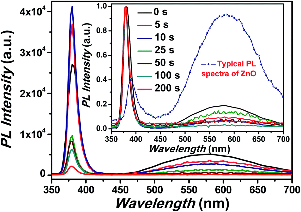 | ||
| Fig. 3 PL spectra of pristine and Cr coated ZnO NRs. The inset shows the normalized PL spectra. Inset also shows the typical PL spectra of ZnO grown using hydrothermal process. | ||
| Sputtering time | UV peak position (nm) | Visible peak position (nm) | FWHM of UV peak (nm) |
|---|---|---|---|
| 0 s | 380.1 | 576.9 | 18.6 |
| 5 s | 380.0 | 586.1 | 13.0 |
| 10 s | 379.8 | 589.9 | 13.8 |
| 25 s | 379.8 | 590.1 | 12.8 |
| 50 s | 378.9 | 590.0 | 13.4 |
| 100 s | 378.8 | 594.2 | 13.5 |
| 200 s | 378.6 | 592.4 | 14.4 |
It is interesting to note here that, with Cr coating, suppression in DLE with peak position mainly in the orange region of the visible spectra has been observed. The DLE peak positions are mentioned in the Table 1 and have indicated strong red shift from the peak position corresponding to the pristine sample. This gradual red shift of the DLE peak position with Cr sputtering time clearly indicates that  and
and  states got passivated significantly, while Cr coating does not play significant role for the passivation of defect states belonging to the doubly ionized oxygen emissions (
 ).63 In general, the suppression of the DLE has been attributed to the transfer of electrons from defect states to the metal Fermi level and coupling between excitons and surface plasmons.19 Although this mechanism seems satisfactory for metals having work function below to the defect states of ZnO.41 Now, it is worthwhile to note here that Cr forms Schottky contacts with ZnO, hence the ZnO conduction band level (4.3 eV) will lie above to the Cr Fermi level (4.5 eV), thereby theoretically resulting into the band bending at interface which would definitely suppress the NBE and DLE emission.23 However, the contradictory observation of the enhancement of NBE in the PL spectra supports our assumption of plasmon–exciton coupling. It is important to mention here that the existence of plasmon resonance in Cr is highly related to the interband transitions and therefore get affected by it. As can be seen from Fig. 3 that the NBE emission enhancement ratio is nearly 1.5 for Cr coated (10 s) ZnO NRs. Although there is an enhancement in the value of the NBE however it is lower than the typical values of the enhancement ratio that were reported for other metals like Au, Ag, Pt and Al.25,26,64,65 It is worth to mention here that the exciton–plasmon coupling strength depends prominently on the magnitude of the real part of dielectric constant of the metal (the real part of the dielectric constant of the metal must be negative and its magnitude must be greater than that of the semiconductor). For Cr, the magnitude value of the real part of dielectric constant is not as large as for the other plasmonic metals like Ag, Au and Al in the UV and visible region of the electromagnetic spectra, therefore, it is expected that the effect of plasmon coupling will be less pronounced in the case of Cr.61 However, the plasmon–exciton coupling efficiency can be remarkably modified by varying the shape and size of nanoparticles of metals. Hence, the plasmon resonance peak and thus the coupling between plasmons and excitons can be improved significantly with the variation of size and shape of Cr NPs.27
In order to provide a plausible justification of the above mentioned results, we have proposed the involvement of hot carriers either generated through the decay of surface plasmons or interband transitions as a dominating contributor for the NBE enhancement and DLE passivation.55,66 Illumination of metallic nanoparticles with appropriate sources produces strong optical near-fields that initiate a series of processes with multiple outcomes, including the excitation of surface plasmons, their radiative decay to photons and non-radiative decay into hot carriers.67 These carriers are considered as hot carriers, since these have significantly large energy than those of thermal excitations at ambient temperatures.68 Further, these carriers can be injected into semiconductor as Landau damping of the collective oscillation of these electrons can result into highly energetic carriers and therefore can significantly increase the probability of transfer of these hot carriers into the semiconductor.69 Hot carrier generation through non-radiative decay of surface plasmons at metal semiconductor interface can occur either through direct or phonon assisted transitions. This process is typically allowed above the interband threshold energy of the given metal.70 Interestingly, in the case of Cr the direct transition occur from the d-band to the unoccupied state above the Fermi level, which results in generation of hot holes (in d-bands), which usually are ∼1–2 eV more energetic than the hot electrons.27 Subsequently, upon generation plasmons undergo fast de-phasing with the creation of electron–hole pairs. Plasmon de-phasing comes from collisions with phonons and defects along with electron–electron scattering. There is a significant probability of non-radiative decay of these plasmons, thus the fluorescence quantum yield is very low.
It is interesting to mention here that plasmon resonance also takes place in Cr as have been mentioned earlier in the absorption spectra of Cr film (transitions from the Fermi surface to the flat unoccupied band). Thus, both surface plasmon decay and interband transitions will generate hot holes in the d-bands and hot electrons in sp bands. This hot interband electron–hole pair generation can lead to the hot electron injection into the CB of ZnO NRs thus will enhance the NBE emission. Interestingly the hot holes can easily recombine with the electrons present at the  ,
,  states, which results into the suppression of DLE corresponding to the blue and green region of visible spectra. It can be clearly seen that the hot hole levels are actually below to the ZnO defect levels, and thus can provide energetically favourable path for recombination of the electrons present at the defect levels with hot holes further leading to the suppression of defect related emissions primarily in the blue and green region of the emission spectra of ZnO. In addition to this, hot electrons can directly go to the ZnO conduction band level which could lead to NBE enhancement along with the contribution due to plasmonic transitions and exciton–plasmon coupling. Thus it can be stated that hot electrons can play major role in NBE enhancement while hot holes in DLE passivation in the case of Cr coated ZnO NRs. Strikingly, hot carrier generation through interband transitions play a major role in comparison to that of the hot carrier generation through plasmon decay.27 The schematic of the above mentioned mechanism is shown in Fig. 4.
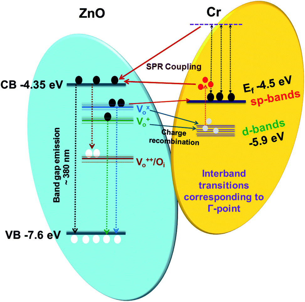 | ||
| Fig. 4 Schematic diagram for the mechanism of the emission enhancement in Cr coated ZnO NRs. | ||
To gain better understanding of the mechanism of the above mentioned phenomenon, we have calculated the enhancement ratio for Cr-coated ZnO NRs with different sputtering time. From Fig. 5, it has been observed that the enhancement ratio start increasing with the increase in the Cr-sputtering time. Moreover, it reached to a maximum value of nearly 1.5-fold for a sputtering time of 10 s. Surprisingly, it starts to decrease subsequently for sputtering times over 10 s. The increase of enhancement ratio can be simply attributed to the increased coupling between the DLE of ZnO with the SPs of Cr NPs and hot carriers at the interface. It is obvious to interpret that the plasmon–exciton coupling strength increases with increasing coverage of Cr NPs on ZnO NRs. Plasmon–exciton coupling is highly sensitive to metal shape, size and density and can be controlled by the sputtering time. Capping Ag films on InGaN/GaN quantum well and Au-coated films on ZnCdO thin films for enhancement of spontaneous emission have been already demonstrated by scientific groups.71,72 It was clearly shown by Zhang et al. that there exist an optimum density of metal NPs for best value of enhancement of PL71,72 Therefore in the case of Cr also there should be a minimal density of Cr NPs for obtaining the maximum enhancement ratio as can be seen from Fig. 6. Generally, the trade-off between absorption, scattering and plasmon coupling of metal NPs play a critical role in the governance of plasmon–exciton coupling. When the density of Cr NPs becomes larger than the trade-off density of the metal NPs, absorption of Cr NPs and phononic transitions at the interface could gradually dominate the process.
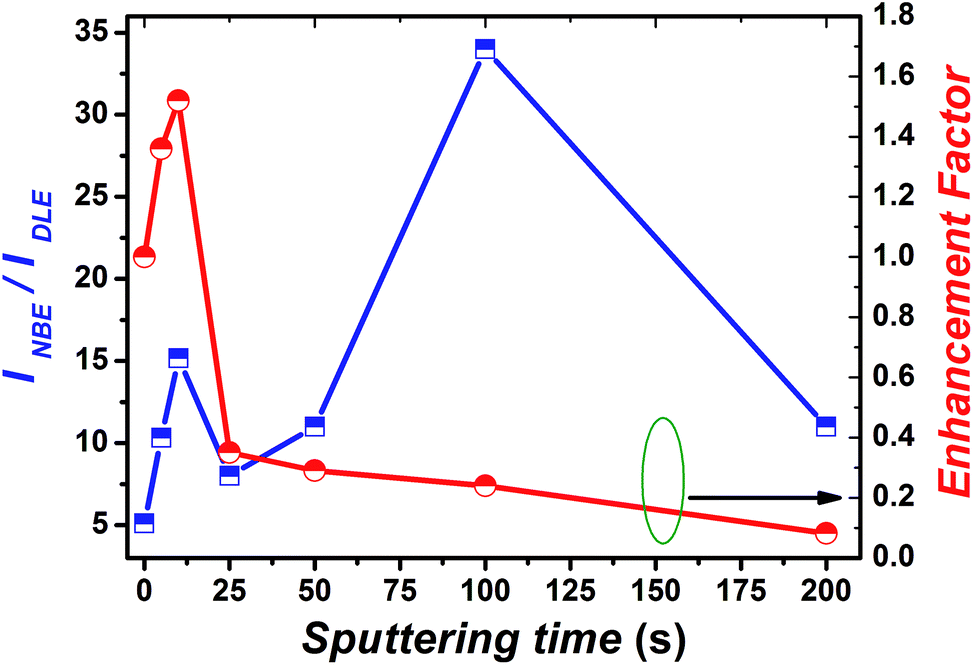 | ||
| Fig. 5 Dependence of the ratio of PL intensity corresponding to NBE and DLE and enhancement factor on the Cr sputtering time. | ||
 | ||
| Fig. 6 Schematic diagram for the mechanism of the involvement of phononic transitions on the emissions of pristine and metal coated ZnO NRs (10 and 100 s). | ||
In general, photo-generated excitons in semiconductors decay through both radiative and non-radiative recombination processes as have been shown in Fig. 6. Mathematically, the PL decay time (τZnO) of bare ZnO NRs can be therefore expressed as:


Thus, the PL decay time (τCr/ZnO) will decrease due to plasmon coupling to some extent and can be expressed as  and
and  . Where,
  and
and  are the non-radiative and radiative decay times of Cr coated ZnO NRs, respectively. 1/τSP is the plasmon–exciton coupling rate.74 A significant decrease in the PL decay time can be expected for Cr/ZnO primarily due to the defect-SP coupling, compared to that of the pristine ZnO NRs.75 The above mentioned qualitative analysis have suggested that the τCr/ZnO will gradually decrease with increasing density of Cr particles over ZnO NRs as shown in Fig. 6. Alternatively, the stronger the local SP field became, the more would be the probability of the scattering by the rough surface of Cr. Thus, the coupled energy could become significant, thereby exciting the more coupled SP polaritons into free space to take part in radiative recombination via scattering (Fig. 6).74 With Cr sputtering time of more than 10 s, we deduced that some Cr NPs began to coalesce together. This is a typical Ostwald ripening, as shown in Fig. 6 for the case of Cr coating for 100 s. At this stage the intense absorption would dominate the scattering process, leading to an enhancement of non-radiative recombination. This increased non-radiative recombination rate also supports the previously observed low enhancement ratio in the case of Cr coating in comparison to other metals (as has been observed from the PL spectra). Additionally, capping of ZnO surfaces with metal films may cause a reduction of density of surface recombination centers consequently can lead to an increase of the NBE emission. Therefore, the probabilities of radiative trap recombination at the surface defects will decrease when the surface is passivated by capping a metal layer which will eventually, decrease the probabilities of radiative trap recombination.
Excitation intensity dependent PL spectra can also shed some light on the effect of Cr coating over the passivation of defects. Dependence of the emission spectra of as-synthesized ZnO samples on the laser excitation intensity has been shown in Fig. 7. It has been established that the luminescence intensity I can be expressed as:
| I = ηI0α |
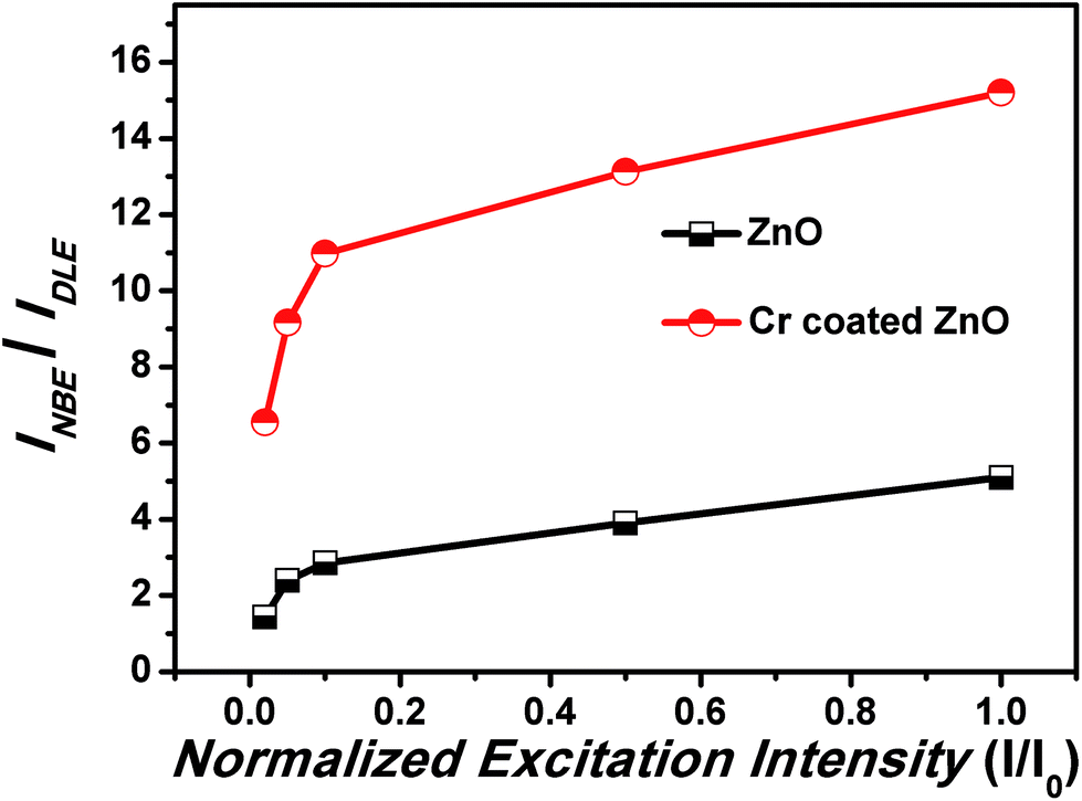 | ||
| Fig. 7 Dependence of the ratio of PL intensity corresponding to NBE and DLE and enhancement factor on the excitation intensity. | ||
In this relation I0 is the power of the excitation laser radiation (10 mW in this case), η is the emission efficiency and the exponent α represents the type of radiative recombination mechanism.62 For the excitation-intensity variations of the NBE emission intensity acquired at 293 K, the exponent α has a value at around 1.5 for the pristine samples and 1.68 for Cr coated ZnO NRs, hence indicating more enhanced band gap emission with Cr coating.62 The increase in the value of α is an indication of passivation of defects. Moreover, a blue shift of 4 nm, in the UV peak positions was observed, therefore the effect of laser induced heating can be discarded in both cases. In order to have a thorough insights into the effect of excitation intensity on the Cr coated ZnO NRs PL, we have analysed the variation of INBE/IDLE vs. excitation intensity (shown in Fig. 7). A significant change has been observed in INBE/IDLE with the variation of excitation intensity. A significant decrease in the value of the INBE/IDLE has been observed at low excitation intensities for the case of as synthesized ZnO NRs as well as for the Cr coated ZnO NRs.
Fig. 8(a) shows confocal-microscope images of the pristine ZnO NRs (under illumination by a 488 nm laser) captured over the range of 500–650 nm in order to systematically analyze the DLE. The confocal-microscope measurements were conducted to investigate the variation in the fluorescence intensity mainly in the visible region due to the coating of Cr layer over the ZnO NRs.35 The confocal-microscope images (Fig. 8(b)) show a suppressed DLE from the ZnO NRs coated with Cr using sputtering. The intensity of the selected regions has been shown in Fig. 8(c and d) for pristine ZnO NRs, and Cr coated ZnO NRs. The intensity values for Cr coated ZnO NRs were nearly at noise level and were in well resemblance with PL results.
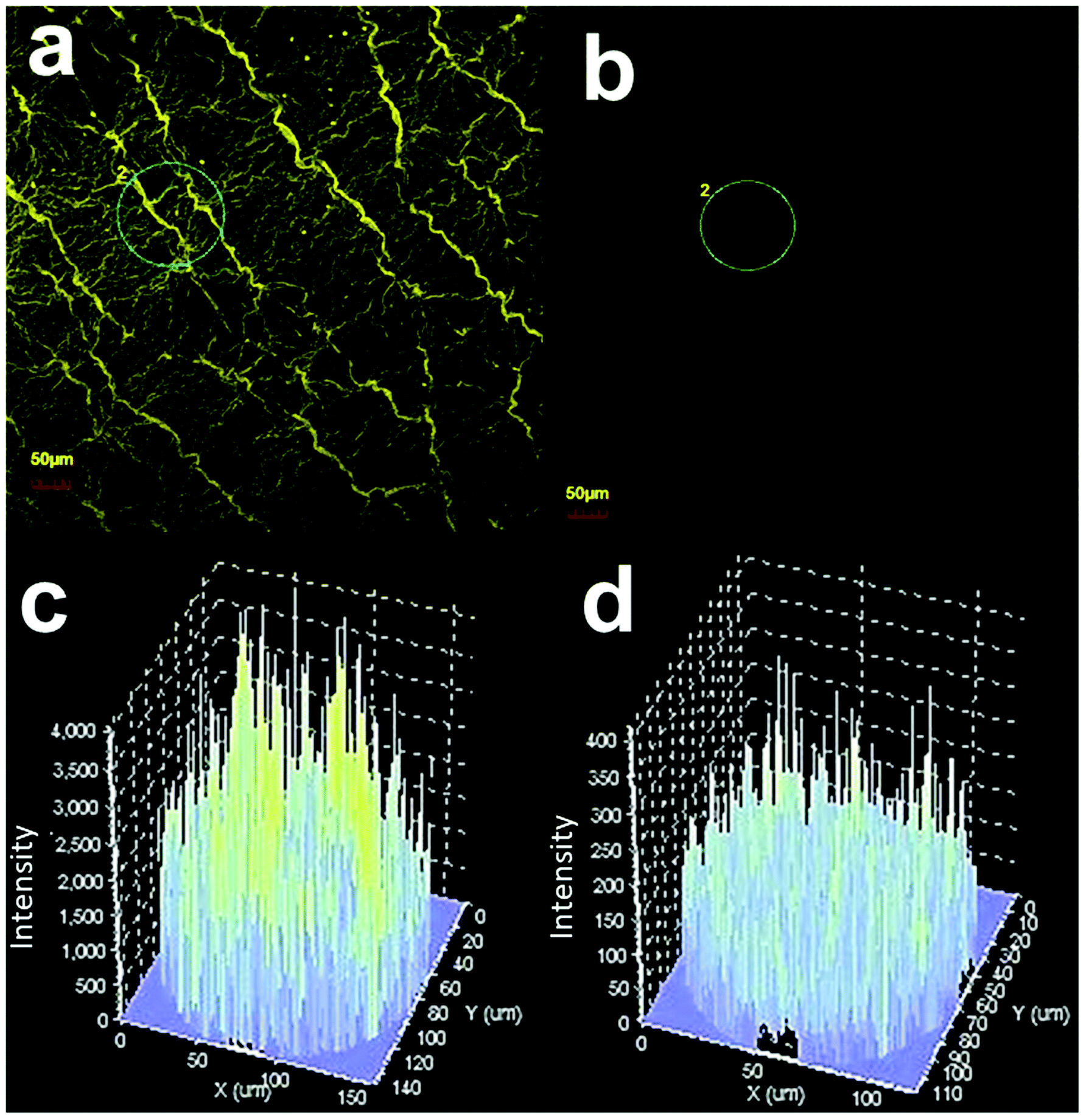 | ||
| Fig. 8 Confocal microscopy images of the pristine and Cr coated ZnO samples. | ||
Wurtzite structured ZnO belongs to P63mc symmetry group and consists of two zinc and two oxygen atoms in a unit cell with twelve phonon modes (of which nine are optically active).76 At Γ point of reciprocal space, phonon modes are represented as:
| Γout = A1 + 2B1 + E1 + 2E2 |
In wurtzite ZnO crystals, the non-polar phonon modes with symmetry E2 have two frequencies, E2 (high) is associated with oxygen atoms while E2(low) is associated with Zn defects.77 Fig. 9 shows the Raman spectra of pristine and Cr coated ZnO samples (for 10 s). The usual modes in ZnO, such as 333 cm−1 (E2(high) − E2(low)) and 437 cm−1 (E2(high)), were observed.56 The peak at 375 cm−1 can be assigned to A1(TO) mode.78 In addition to this a peak was observed at 410 cm−1 and can be attributed to E1(TO) modes. The peak at 500 cm−1 can be attributed to the disorder activated Raman scattering of silent mode 2-B2L.56 Moreover, the peak at 579 cm−1 has been observed and can be assigned to the longitudinal optical (LO) mode.29 The 579 cm−1 band i.e. E1(LO) mode can be assigned to defect states like, oxygen vacancies, Zn interstitials. It is well reported that this peak has strong dependence on the surface electric field and hence can be modulated using metal NPs.79 Interestingly both broadening and increase in the intensity of the peak corresponding to E1(LO) mode was observed in case of Cr coated ZnO NRs (Cr coating for 10 seconds), clearly demonstrating the fact that electron–phonon coupling strength is diminishing in case of coating of Cr. The peaks at 525 and 564 cm−1 can be assigned to 2LA and A1(LO) modes respectively.78 Additionally, the peak at 470 cm−1 can be assigned to the surface optical (SO) mode of ZnO.80 SO phonons may be generated at the interface between different materials with different dielectric constants and propagate along the interface. Their frequencies are located between the frequencies of the transverse optical (TO) and LO modes, and are expected to show a very dispersive behaviour regarding the dielectric constant of the outer medium.81 The increase in the intensity of the SO mode after Cr coating suggests the passivation of surface states with metal coating.81
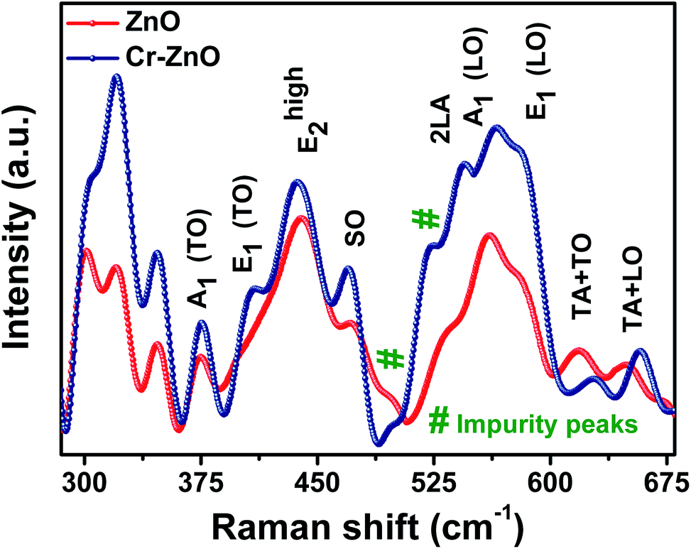 | ||
| Fig. 9 Raman spectra of pristine and Cr coated ZnO NRs. Here Cr was sputtered for 10 s using rf-sputtering. | ||
Until now, we have focused on the effect of Cr coating over the passivation of DLE and simultaneous enhancement in the NBE towards UV only emission. Another interesting issue with ZnO nanostructures lies in their utilization for intense and broad visible region emission. The selective tuning of the visible emission in the ZnO is not well addressed in the literature. Here, we have performed the annealing of the Cr coated samples at 500 °C (shown in Fig. 10(a)) for selectively tuning the visible light emission. Interestingly, it can be seen that the UV emission intensity decreases upon annealing and becomes diminished for the samples with Cr coating for more than 25 seconds. In addition to this, broader peak encompassing visible region with increase in the intensity value was observed by increasing the Cr sputtering time. Thus, these results indicate that a supply of thermal energy after Cr-sputtering affects the UV emission intensity. The PL results, therefore, support our proposition that it is the temperature which plays a key role in the modulation of the emission properties. The occupation of oxygen vacancies with annealing by Cr ions and formation and oxygen interstitials can be assigned for the significant enhancement of the DLE.82,83 Fig. 10(b–d) show the de-convoluted PL spectra of samples annealed at 500 °C after coating Cr for 5, 10 and 25 seconds respectively. Interestingly, an enhancement and broadening in the emission spectra corresponding to orange, red and NIR regions can be clearly seen. The peak at 630 and 685 nm can be assigned to oxygen interstitials and antisite defects.7,75 Conclusively, the post sputtering annealing has selectively enhanced the DLE with the increase in Cr sputtering time. The above mentioned enhancement of DLE in a controlled manner can be helpful for photo-catalytic activity and ZnO based LEDs emitting in the visible region of the spectrum.
 | ||
| Fig. 10 (a) PL spectra of Cr coated ZnO NRs annealed at 500 °C after Cr coating. (b–d) de-convoluted PL spectra of samples with Cr sputtering time 5, 10 and 25 seconds respectively. | ||
3.3 Device characterization
The photo-response of pristine/Cr coated ZnO NRs has been studied under illumination using a lateral photodetector device configuration. I–V characteristics of ZnO and Cr coated ZnO devices were measured under dark and illumination of green light (λ = 530 nm and intensity = 5 mW cm−2) illumination are shown in Fig. 11. A typical characteristic of a photodetector was observed with an overall increment in the current level with the increasing bias in between the lateral Ag electrodes. In addition to this it was clearly observed that the dark current of the photoconductor was significantly reduced with Cr coating (for 10 seconds sputtering). This decrease in dark current can be attributed to the formation of Schottky contact at the interface of Cr and ZnO nanorods. The dark current values were observed to be 0.10, 0.02 μA for pristine and Cr (for 10 s sputtering) coated ZnO NRs respectively.84 In the dark, oxygen molecules generally get adsorbed on the surface of ZnO NRs and capture the free electrons [O2 + e− → O2−] thus, a depletion layer with low conductivity is created near the surface.85,86 After covering with Cr particles, the surface states and the adsorption of oxygen molecules do not change due to that Cr particles do not cover the whole surface of the NRs and the contact region between Cr and ZnO is very small.87 Additionally, since the work function of ZnO (4.1 eV) is lower than that of Cr (4.5 eV), electrons will flow from ZnO to Cr which can lead to the formation of Schottky barrier at the interface. The negatively charged Cr nanoparticle depletes the carriers near the surface of ZnO nanowires. Notably, the width of depletion layer is related to barrier height, depletion region near the Cr nanoparticle is larger than that at defect and adsorbed oxygen site. The formation of the large depletion region is the main reason for the decrease in the dark current after covering with Cr nanoparticles. However, Cr coated samples with sputtering time of 50 s it was observed that the dark current level got increased and that can be assigned to the formation of continuity of Cr agglomerates. The results clearly showed that with Cr coating dark current level can be significantly reduced, thereby suggesting its potential for transistor applications also, as lower dark current level is required to get higher ON/OFF ratio. | ||
| Fig. 11 (a) The current (I)–voltage (V) characteristics of the pristine and Cr coated ZnO nanorods (b) Cr coated ZnO NRs based photodetector in the dark and under green light illumination. | ||
Further, the photoconductivity of Cr coated ZnO NRs based device was found to be enhanced over the pristine ZnO device under the same measurement condition for visible light. Typically, ZnO is not sensitive for visible light therefore it lacks visible light detection. The origin of enhanced visible photo-response of Cr coated ZnO NRs was a result of the inter-band transition of Cr d-band electrons as an effect of the illumination of visible light.84 The filled d-band in Cr, below the Fermi level provides large number of electrons for interband transition under visible light illumination. Upon green light excitation, the d-band electrons of Cr atoms were excited to the conduction band with a final transfer to ZnO NRs due to the presence of electric field at the metal–semiconductor junction formed between Cr and ZnO. The combined effects of electrons transfer due to interband transition and plasmon resonance have resulted into increased photoconductivity in the green region.84,88
4. Conclusions
The NBE emission and DL emission of ZnO NRs are enhanced and suppressed, respectively, by Cr coating, which can be attributed to a combination of hot electron transfer from Cr-sp band to ZnO conduction band and recombination of electrons at defect levels with hot holes present at d band of Cr. Moreover, charge recombination can be assigned for suppression of the defect emissions corresponding to the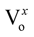 and
and  assisted emissions in the case of Cr. Interband transitions present in the metal have been shown to have strong influence on the emission properties. KM absorption spectra have confirmed the interband transitions nearly at 1.56 eV for Cr. We further believe that the utilization of Cr plasmonics for passivation of defect states of ZnO NRs will play a significant role towards the development of highly efficient optoelectronic devices.
Conflicts of interest
There are no conflicts to declare.Acknowledgements
One of the authors T. D. is grateful to FESEM, XRD, and PL and confocal microscopy facilities equipped at the Sophisticated Instrument Centre, IIT Indore. T. D. would further like to thank the Ministry of Human Resource and Development, India for providing the Teaching Assistantship. Authors would further like to acknowledge Dr P. R. Sagdeo for allowing the usage of UV visible DRS facility.References
- S. Xu and Z. L. Wang, One-Dimensional ZnO Nanostructures: Solution Growth and Functional Properties, Nano Res., 2011, 4(11), 1013–1098 CrossRef CAS.
- U. Ozgur, Y. I. Alivov, C. Liu, A. Teke, M. A. Reshchikov, S. Dogan, V. Avrutin, S. J. Cho and H. Morkoc, A Comprehensive Review of ZnO Materials and Devices, J. Appl. Phys., 2005, 98(4), 1–103 CrossRef.
- D. P. Volanti, M. O. Orlandi, J. Andres and E. Longo, Efficient Microwave-Assisted Hydrothermal Synthesis of CuO Sea Urchin-like Architectures via a Mesoscale Self-Assembly, CrystEngComm, 2010, 12(6), 1696–1699 RSC.
- Y. H. Park, Y. H. Shin, S. J. Noh, Y. Kim, S. S. Lee, C. G. Kim, K. S. An and C. Y. Park, Optical Quenching of NiONi Coated ZnO Nanowires, Appl. Phys. Lett., 2007, 91(1), 1–4 Search PubMed.
- A. Furube, T. Asahi, H. Masuhara, H. Yamashita and M. Anpo, Charge Carrier Dynamics of Standard TiO2 Catalysts Revealed by Femtosecond Diffuse Reflectance Spectroscopy, J. Phys. Chem. B, 1999, 103, 3120–3127 CrossRef CAS.
- W. Tian, C. Zhang, T. Zhai, S.-L. Li, X. Wang, M. Liao, K. Tsukagoshi, D. Golberg and Y. Bando, Flexible SnO2 Hollow Nanosphere Film Based High-Performance Ultraviolet Photodetector, Chem. Commun., 2013, 49(36), 3739–3741 RSC.
- A. B. Djuriić and Y. H. Leung, Optical Properties of ZnO Nanostructures, Small, 2006, 2(8–9), 944–961 CrossRef PubMed.
- A. B. Djuriić, A. M. C. Ng and X. Y. Chen, ZnO Nanostructures for Optoelectronics: Material Properties and Device Applications, Prog. Quantum Electron., 2010, 34(4), 191–259 CrossRef.
- W. Z. Liu, H. Y. Xu, C. L. Wang, L. X. Zhang, C. Zhang, S. Y. Sun, J. G. Ma, X. T. Zhang, J. N. Wang and Y. C. Liu, Enhanced Ultraviolet Emission and Improved Spatial Distribution Uniformity of ZnO Nanorod Array Light-Emitting Diodes via Ag Nanoparticles Decoration, Nanoscale, 2013, 5(18), 8634–8639 RSC.
- D. Vanmaekelbergh and L. K. van Vugt, ZnO Nanowire Lasers, Nanoscale, 2011, 3(7), 2783–2800 RSC.
- T. Dixit, A. Bilgaiyan, I. A. Palani, D. Nakamura, T. Okada and V. Singh, Influence of Potassium Permanganate on the Anisotropic Growth and Enhanced UV Emission of ZnO Nanostructures Using Hydrothermal Process for Optoelectronic Applications, J. Sol-Gel Sci. Technol., 2015, 75(3), 693–702 CrossRef CAS.
- T. Dixit, I. A. Palani and V. Singh, Investigation on the Influence of Dichromate Ion on the ZnO Nano-Dumbbells and ZnCr2O4 Nano-Walls, J. Mater. Sci.: Mater. Electron., 2014, 26(2), 821–829 CrossRef.
- K. H. Tam, A. B. Djurišić, C. M. N. Chan, Y. Y. Xi, C. W. Tse, Y. H. Leung, W. K. Chan, F. C. C. Leung and D. W. T. Au, Antibacterial Activity of ZnO Nanorods Prepared by a Hydrothermal Method, Thin Solid Films, 2008, 516(18), 6167–6174 CrossRef CAS.
- W. Wang, Q. Zhao, J. Xu and D. Yu, A Unique Strategy for Improving Top Contact in Si/ZnO Hierarchical Nanoheterostructure Photodetectors, CrystEngComm, 2012, 14(9), 3015 RSC.
- Q.-H. Ren, Y. Zhang, H.-L. Lu, H.-Y. Chen, Y. Zhang, D.-H. Li, W.-J. Liu, S.-J. Ding, A.-Q. Jiang and D. W. Zhang, Surface-Plasmon Mediated Photoluminescence Enhancement of Pt-Coated ZnO Nanowires by Inserting an Atomic-Layer-Deposited Al2O3 Spacer Layer, Nanotechnology, 2016, 27(16), 165705 CrossRef PubMed.
- X. L. Yu, H. M. Ji, H. L. Wang, J. Sun and X. W. Du, Synthesis and Sensing Properties of ZnO/ZnS Nanocages, Nanoscale Res. Lett., 2010, 5(3), 644–648 CrossRef CAS PubMed.
- C. Zhang, H. Y. Xu, W. Z. Liu, L. Yang, J. Zhang, L. X. Zhang, J. N. Wang, J. G. Ma and Y. C. Liu, Enhanced Ultraviolet Emission from Au/Ag-nanoparticles@MgO/ZnO Heterostructure Light-Emitting Diodes: A Combined Effect of Exciton- and Photon-Localized Surface Plasmon Couplings, Opt. Express, 2015, 23(12), 15565 CrossRef CAS PubMed.
- Y. K. Mishra, V. S. K. Chakravadhanula, V. Hrkac, S. Jebril, D. C. Agarwal, S. Mohapatra, D. K. Avasthi, L. Kienle and R. Adelung, Crystal Growth Behaviour in Au-ZnO Nanocomposite under Different Annealing Environments and Photoswitchability, J. Appl. Phys., 2012, 112(6), 064308 CrossRef.
- S. Park, Y. Mun, S. An, W. In Lee and C. Lee, Enhanced Photoluminescence of Au-Functionalized ZnO Nanorods Annealed in a Hydrogen Atmosphere, J. Lumin., 2014, 147, 5–8 CrossRef CAS.
- A. E. Rakhshani, Visible Light Emission and UV Light Detection Properties of Solution-Grown ZnO/polymer Heterojunction Diodes on Stainless Steel Foil, Appl. Surf. Sci., 2014, 311, 614–620 CrossRef CAS.
- K. W. Liu, R. Chen, G. Z. Xing, T. Wu and H. D. Sun, Photoluminescence Characteristics of High Quality ZnO Nanowires and Its Enhancement by Polymer Covering, Appl. Phys. Lett., 2010, 96(2), 1–4 CrossRef.
- K. Okamoto, I. Niki, A. Shvartser, Y. Narukawa, T. Mukai and A. Scherer, Surface-Plasmon-Enhanced Light Emitters Based on InGaN Quantum Wells, Nat. Mater., 2004, 3(9), 601–605 CrossRef CAS PubMed.
- Y. J. Fang, J. Sha, Z. L. Wang, Y. T. Wan, W. W. Xia and Y. W. Wang, Behind the Change of the Photoluminescence Property of Metal-Coated ZnO Nanowire Arrays, Appl. Phys. Lett., 2011, 98(3), 14–17 CrossRef.
- C. K. N. Peh, L. KE and G. W. Ho, Modification of ZnO Nanorods through Au Nanoparticles Surface Coating for Dye-Sensitized Solar Cells Applications, Mater. Lett., 2010, 64(12), 1372–1375 CrossRef CAS.
- J. M. Lin, H. Y. Lin, C. L. Cheng and Y. F. Chen, Giant Enhancement of Bandgap Emission of ZnO Nanorods by Platinum Nanoparticles, Nanotechnology, 2006, 17(17), 4391–4394 CrossRef.
- M. Mahanti and D. Basak, Highly Enhanced UV Emission due to Surface Plasmon Resonance in Ag-ZnO Nanorods, Chem. Phys. Lett., 2012, 542, 110–116 CrossRef CAS.
- D. Manchon, J. Lermé, T. Zhang, A. Mosset, C. Jamois, C. Bonnet, J.-M. Rye, A. Belarouci, M. Broyer and M. Pellarin, et al., Plasmonic Coupling with Most of the Transition Metals: A New Family of Broad Band and Near Infrared Nanoantennas, Nanoscale, 2015, 7(3), 1181–1192 RSC.
- Y. Fang, Y. Wang, L. Gu, R. Lu and J. Sha, Effect of the Defect on Photoluminescence Property of Al-Coated ZnO Nanostructures, Opt. Express, 2013, 21(3), 3492–3500 CrossRef CAS PubMed.
- Q. J. Ren, S. Filippov, S. L. Chen, M. Devika, N. Koteeswara Reddy, C. W. Tu, W. M. Chen and I. A. Buyanova, Evidence for Coupling between Exciton Emissions and Surface Plasmon in Ni-Coated ZnO Nanowires, Nanotechnology, 2012, 23(42), 425201 CrossRef CAS PubMed.
- X. An, Z. Zhang, J. Song, Y. Liu, X. Li, Y. He, C. Gong and E. Xie, Morphology Tailored Surface Plasma Emission of Titanium Capped ZnO Films, Mater. Lett., 2011, 65(23–24), 3552–3554 CrossRef CAS.
- M. K. Lee and H. F. Tu, Optical Emissions of Zn and ZnO in Zn-ZnO Structure Synthesized by Electrodeposition with Aqueous Solution of Zinc Nitrate-6-hydrate, Cryst. Growth Des., 2008, 8(6), 1785–1788 CAS.
- Z. Y. Tan, D. W. Y. Yong, Z. Zhang, H. Y. Low, L. Chen and W. S. Chin, Nanostructured Cu/ZnO Coupled Composites: Toward Tunable Cu Nanoparticle Sizes and Plasmon Absorption, J. Phys. Chem. C, 2013, 117(20), 10780–10787 CAS.
- T. Thio, H. F. Ghaemi, H. J. Lezec, P. a. Wolff and T. W. Ebbesen, Surface-Plasmon-Enhanced Transmission through Hole Arrays in Cr Films, J. Opt. Soc. Am. B, 1999, 16(10), 1743 CrossRef CAS.
- M. D. L. Ruiz Peralta, U. Pal and R. S. Zeferino, Photoluminescence (PL) Quenching and Enhanced Photocatalytic Activity of Au-Decorated ZnO Nanorods Fabricated through Microwave-Assisted Chemical Synthesis, ACS Appl. Mater. Interfaces, 2012, 4(9), 4807–4816 CAS.
- A. Asok, M. N. Gandhi and A. R. Kulkarni, Enhanced Visible Photoluminescence in ZnO Quantum Dots by Promotion of Oxygen Vacancy Formation, Nanoscale, 2012, 4(16), 4943 RSC.
- Z. Wang, F. Wang, Y. Cui, X. Li, A. M. Toufiq, Y. Lu and Q. Li, Novel Method to Enhance the Visible Emission of ZnO Nanostructures, Chem. Phys. Lett., 2014, 614, 53–56 CrossRef CAS.
- M. T. Qamar, M. Aslam, I. M. I. Ismail, N. Salah and A. Hameed, Synthesis, Characterization, and Sunlight Mediated Photocatalytic Activity of CuO Coated ZnO for the Removal of Nitrophenols, ACS Appl. Mater. Interfaces, 2015, 7(16), 8757–8769 CAS.
- S. T. Kochuveedu, Y. H. Jang and D. H. Kim, A Study on the Mechanism for the Interaction of Light with Noble Metal-Metal Oxide Semiconductor Nanostructures for Various Photophysical Applications, Chem. Soc. Rev., 2013, 42(21), 8467–8493 RSC.
- M. Khenfouch, M. Baïtoul and M. Maaza, White Photoluminescence from a Grown ZnO Nanorods/graphene Hybrid Nanostructure, Opt. Mater., 2012, 34(8), 1320–1326 CrossRef CAS.
- A. Janotti and C. G. Van De Walle, Native Point Defects in ZnO, Phys. Rev. B: Condens. Matter Mater. Phys, 2007, 76(16), 1–22 CrossRef.
- T. Dixit, I. A. Palani and V. Singh, Role of Surface Plasmon Decay Mediated Hot Carriers toward the Photoluminescence Tuning of Metal-Coated ZnO Nanorods, J. Phys. Chem. C, 2017, 121(6), 3540–3548 CAS.
- X. Kong, X. Sun, X. Li and Y. Li, Catalytic Growth of ZnO Nanotubes, Mater. Chem. Phys., 2003, 82(3), 997–1001 CrossRef CAS.
- P. Sagar, P. K. Shishodia, R. M. Mehra, H. Okada, A. Wakahara and A. Yoshida, Photoluminescence and Absorption in Sol-Gel-Derived ZnO Films, J. Lumin., 2007, 126(2), 800–806 CrossRef CAS.
- B. Gil, Oscillator Strengths of A, B, and C Excitons in ZnO Films, Phys. Rev. B, 2001, 64(20), 5–7 CrossRef.
- J. Petersen, C. Brimont, M. Gallart, O. Crégut, G. Schmerber, P. Gilliot, B. Hönerlage, C. Ulhaq-Bouillet, J. L. Rehspringer and C. Leuvrey, et al., Structural and Photoluminescence Properties of ZnO Thin Films Prepared by Sol-Gel Process, J. Appl. Phys., 2008, 104(11), 113539 CrossRef.
- A. Ali Umar, M. Y. Abd Rahman, R. Taslim, M. Mat Salleh and M. Oyama, A Simple Route to Vertical Array of Quasi-1D ZnO Nanofilms on FTO Surfaces: 1D-Crystal Growth of Nanoseeds under Ammonia-Assisted Hydrolysis Process, Nanoscale Res. Lett., 2011, 6(1), 564 CrossRef PubMed.
- R. M. Sheetz, I. Ponomareva, E. Richter, A. N. Andriotis and M. Menon, Defect-induced optical absorption in the visible range in ZnO nanowires, Phys. Rev. B, 2009, 80, 195314 CrossRef.
- T. Dixit, M. Shukla, I. A. Palani and V. Singh, Insight of Dipole Surface Plasmon Mediated Optoelectronic Property Tuning of ZnO Thin Films Using Au, Opt. Mater., 2016, 62, 1–7 CrossRef.
- S. Schönau, F. Ruske, S. Neubert and B. Rech, Analysis of Urbach-like Absorption Tails in Thermally Treated ZnO:Al Thin Films, Appl. Phys. Lett., 2013, 103(19), 192108 CrossRef.
- N. Debnath, M. Chowdhuri and S. Chatterjee, Electronic Energy Bands and Optical Properties of Cr and Fe by the KKR Method, J. Phys. F: Met. Phys., 1985, 15, 1693 CrossRef CAS.
- L. W. Bos and D. W. Lynch, Optical Properties of Antiferromagnetic Chromium and Dilute Cr-Mn and Cr-Re Alloys, Phys. Rev. B: Solid State, 1970, 2(11), 4567–4577 CrossRef.
- J. P. Colombier, P. Combis, E. Audouard and R. Stoian, Transient Optical Response of Ultrafast Nonequilibrium Excited Metals: Effects of Electron-Electron Contribution to Collisional Absorption, Phys. Rev. E: Stat., Nonlinear, Soft Matter Phys., 2008, 77(3), 1–12 CrossRef PubMed.
- N. I. Kulikov, M. Alouani, M. A. Khan and M. V. Magnitskaya, Self-energy corrections to the ab initio band structure: Chromium, Phys. Rev. B: Condens. Matter Mater. Phys., 1987, 36(2), 929 CrossRef CAS.
- N. W. Ashcroft and K. Sturm, Interband absorption and the optical properties of polyvalent metals, Phys. Rev. B: Solid State, 1971, 3(6), 1898 CrossRef.
- R. Sundararaman, P. Narang, A. S. Jermyn, W. A. Goddard III and H. A. Atwater, Theoretical Predictions for Hot-Carrier Generation from Surface Plasmon Decay, Nat. Commun., 2014, 5, 5788 CrossRef CAS PubMed.
- T. Dixit, I. A. Palani and V. Singh, Selective Tuning of Enhancement in near Band Edge Emission in Hydrothermally Grown ZnO Nanorods Coated with Gold, J. Lumin., 2016, 170, 180–186 CrossRef CAS.
- P. J. Feibelman and D. R. Hamann, Quantum-Size Effects in Work Functions of Free-Standing and Adsorbed Thin Metal Films, Phys. Rev. B: Condens. Matter Mater. Phys., 1984, 29(12), 6463–6467 CrossRef CAS.
- H. L. Skriver and N. M. Rosengaard, Surface Energy and Work Function of Elemental Metals, Phys. Rev. B: Condens. Matter Mater. Phys., 1992, 46(11), 7157–7168 CrossRef CAS.
- J. G. Cook, Surface electromagnetic waves in chromium, Solid State Commun., 1986, 60(7), 549–551 CrossRef CAS.
- J. J. Lu, Y. M. Lu, S. I. Tasi, T. L. Hsiung, H. P. Wang and L. Y. Jang, Conductivity Enhancement and Semiconductor-Metal Transition in Ti-Doped ZnO Films, Opt. Mater., 2007, 29(11), 1548–1552 CrossRef CAS.
- D. Barchiesi and T. Grosges, Fitting the Optical Constants of Gold, Silver, Chromium, Titanium, and Aluminum in the Visible Bandwidth, J. Nanophotonics, 2014, 8(1), 83097 CrossRef.
- T. Dixit, I. A. Palani and V. Singh, Hot Holes behind the Improvement in Ultraviolet Photoresponse of Au Coated ZnO Nanorods, Mater. Lett., 2016, 181, 183–186 CrossRef CAS.
- Z. M. Liao, H. Z. Zhang, Y. B. Zhou, J. Xu, J. M. Zhang and D. P. Yu, Surface Effects on Photoluminescence of Single ZnO Nanowires, Phys. Lett. A, 2008, 372(24), 4505–4509 CrossRef CAS.
- D. Zhang, H. Ushita, P. Wang, C. Park, R. I. Murakami, S. C. Yang and X. Song, Photoluminescence Modulation of ZnO via Coupling with the Surface Plasmon Resonance of Gold Nanoparticles, Appl. Phys. Lett., 2013, 103(9), 2011–2016 Search PubMed.
- J. Lu, J. Li, C. Xu, Y. Li, J. Dai, Y. Wang, Y. Lin and S. Wang, Direct Resonant Coupling of Al Surface Plasmon for Ultraviolet Photoluminescence Enhancement of ZnO Microrods, ACS Appl. Mater. Interfaces, 2014, 6(20), 18301–18305 CAS.
- H. Zhang and A. O. Govorov, Optical Generation of Hot Plasmonic Carriers in Metal Nanocrystals: The Effects of Shape and Field Enhancement, J. Phys. Chem. C, 2014, 118(14), 7606–7614 CAS.
- P. Narang, R. Sundararaman and H. A. Atwater, Plasmonic Hot Carrier Dynamics in Solid-State and Chemical Systems for Energy Conversion, Nanophotonics, 2016, 5(1), 96–111 CrossRef CAS.
- M. L. Brongersma, N. J. Halas and P. Nordlander, Plasmon-Induced Hot Carrier Science and Technology, Nat. Nanotechnol., 2015, 10(1), 25–34 CrossRef CAS PubMed.
- T. Barman, A. A. Hussain, B. Sharma and A. R. Pal, Plasmonic Hot Hole Generation by Interband Transition in Gold-Polyaniline, Sci. Rep., 2015, 5, 18276 CrossRef CAS PubMed.
- A. O. Govorov, H. Zhang, H. V. Demir and Y. K. Gun'Ko, Photogeneration of Hot Plasmonic Electrons with Metal Nanocrystals: Quantum Description and Potential Applications, Nano Today, 2014, 9(1), 85–101 CrossRef CAS.
- T. Singh, D. K. Pandya and R. Singh, Surface Plasmon Driven Enhancement in UV-Emission of Electrochemically Grown Zn1-xCdxO Nanorods Using Au Nanoparticles, J. Alloys Compd., 2013, 552, 294–298 CrossRef CAS.
- N. Zhang, W. Tang, P. Wang, X. Zhang and Z. Zhao, In Situ Enhancement of NBE Emission of Au–ZnO Composite Nanowires by SPR, CrystEngComm, 2013, 15(17), 3301 RSC.
- K. W. Liu, Y. D. Tang, C. X. Cong, T. C. Sum, A. C. H. Huan, Z. X. Shen, L. Wang, F. Y. Jiang, X. W. Sun and H. D. Sun, Giant Enhancement of Top Emission from ZnO Thin Film by Nanopatterned Pt, Appl. Phys. Lett., 2009, 94(15), 1–4 Search PubMed.
- B. J. Niu, L. L. Wu, W. Tang, X. T. Zhang and Q. G. Meng, Enhancement of Near-Band Edge Emission of Au/ZnO Composite Nanobelts by Surface Plasmon Resonance, CrystEngComm, 2011, 13(11), 3678 RSC.
- C. W. Cheng, E. J. Sie, B. Liu, C. H. A. Huan, T. C. Sum, H. D. Sun and H. J. Fan, Surface Plasmon Enhanced Band Edge Luminescence of ZnO Nanorods by Capping Au Nanoparticles, Appl. Phys. Lett., 2010, 96(7), 1–4 Search PubMed.
- C. Kranert, R. Schmidt-Grund and M. Grundmann, Surface- and Point-Defect-Related Raman Scattering in Wurtzite Semiconductors Excited above the Band Gap, New J. Phys., 2013, 15, 0–22 CrossRef CAS.
- H. W. Kim, M. A. Kebede and H. S. Kim, Structural, Raman, and Photoluminescence Characteristics of ZnO Nanowires Coated with Al-Doped ZnO Shell Layers, Curr. Appl. Phys., 2010, 10(1), 60–63 CrossRef.
- R. Cuscó, E. Alarcón-Lladó, J. Ibáñez, L. Artús, J. Jiménez, B. Wang and M. J. Callahan, Temperature Dependence of Raman Scattering in ZnO, Phys. Rev. B: Condens. Matter Mater. Phys., 2007, 75(16), 165202 CrossRef.
- H. F. Liu, A. Huang, S. Tripathy and S. J. Chua, Metal-Nanoparticle-Coating-Induced Enhancement and Weakening of Resonant Raman Scattering in ZnO: Effect of Surface Electric Field, J. Raman Spectrosc., 2011, 42(12), 2179–2182 CrossRef CAS.
- S. Filippov, X. J. Wang, M. Devika, N. Koteeswara Reddy, C. W. Tu, W. M. Chen and I. A. Buyanova, Effects of Ni-Coating on ZnO Nanowires: A Raman Scattering Study, J. Appl. Phys., 2013, 113(21), 214302 CrossRef.
- H. F. Liu, S. Tripathy, G. X. Hu and H. Gong, Surface Optical Phonon and A1 (LO) in ZnO Submicron Crystals Probed by Raman Scattering: Effects of Morphology and Dielectric Coating, J. Appl. Phys., 2009, 105(5), 053507 CrossRef.
- M. Mahanti, T. Ghosh and D. Basak, Enhanced Near Band Edge Luminescence of Ti/ZnO Nanorod Heterostructures Due to the Surface Diffusion of Ti, Nanoscale, 2011, 3(10), 4427 RSC.
- L.-C. Chang, H.-L. Kao and K.-H. Liu, Effect of Annealing Treatment on the Electrical Characteristics of Pt/Cr-Embedded ZnO/Pt Resistance Random Access Memory Devices, J. Vac. Sci. Technol., A, 2014, 32(2), 02B119 Search PubMed.
- N. Gogurla, A. K. Sinha, S. Santra, S. Manna and S. K. Ray, Multifunctional Au-ZnO Plasmonic Nanostructures for Enhanced UV Photodetector and Room Temperature NO Sensing Devices, Sci. Rep., 2014, 4, 6483 CrossRef CAS PubMed.
- Y. Q. Bie, Z. M. Liao, H. Z. Zhang, G. R. Li, Y. Ye, Y. B. Zhou, J. Xu, Z. X. Qin, L. Dai and D. P. Yu, Self-Powered, Ultrafast, Visible-Blind UV Detection and Optical Logical Operation Based on ZnO/GaN Nanoscale p-n Junctions, Adv. Mater., 2011, 23(5), 649–653 CrossRef CAS PubMed.
- Y. Li, J. Gong and C. Deng, Hierarchical Structured ZnO Nanorods on ZnO Nanofibers and Their Photoresponse to UV and Visible Lights, Sens. Actuators, A, 2010, 158(2), 176–182 CrossRef CAS.
- K. Liu, M. Sakurai, M. Liao and M. Aono, Giant Improvement of the Performance of ZnO Nanowire Photodetectors by Au Nanoparticles, J. Phys. Chem. C, 2010, 114(46), 19835–19839 CAS.
- J. Lu, C. Xu, J. Dai, J. Li, Y. Wang, Y. Lin and P. Li, Improved UV Photoresponse of ZnO Nanorod Arrays by Resonant Coupling with Surface Plasmons of Al Nanoparticles, Nanoscale, 2015, 7(8), 3396–3403 RSC.
| This journal is © The Royal Society of Chemistry 2018 |