
 Open Access Article
 This Open Access Article is licensed under a Creative Commons Attribution-Non Commercial 3.0 Unported Licence
Mechanisms for low-temperature direct bonding of Si/Si and quartz/quartz via VUV/O3 activation
Jikai Xu,
Chenxi Wang *,
Te Wang,
Yuan Wang,
Qiushi Kang,
Yannan Liu and
Yanhong Tian
*,
Te Wang,
Yuan Wang,
Qiushi Kang,
Yannan Liu and
Yanhong Tian
State Key Laboratory of Advanced Welding and Joining, Harbin Institute of Technology, Harbin 150001, China. E-mail: wangchenxi@hit.edu.cn; Fax: +86-451-86416186; Tel: +86-451-86418359
First published on 23rd March 2018
Abstract
Direct bonding is an attractive technique for joining two mirror polished surfaces without any intermediate materials. Vacuum ultraviolet (VUV) irradiation is an effective way for cleaning surfaces as well as increasing hydrophilicity with less surface damage. However, its applications for the direct bonding of silicon and quartz glasses have seldom been explored. Therefore, in this paper, a vacuum ultraviolet/ozone (VUV/O3) activated direct bonding method for Si/Si and quartz/quartz was developed. A defect-free interface with high bonding strength was achieved after a low-temperature annealing process at 200 °C. According to water contact angle, Raman spectroscopy, atomic force microscopy, and transmission electron microscopy measurements, we demonstrated an understanding of the beneficial surface treatments from VUV irradiation. Then two models for Si/Si and quartz/quartz bonding were established separately based on low-temperature water stress corrosion. Our studies found that the increase of surface roughness with the extension of VUV irradiation time was attributed to the oxide asperities generated on the irradiated surfaces, which possessed strong deformability under the water stress corrosion effect. The excellent bonding benefits from the saturated silanol groups formed on the VUV irradiated surfaces and the positive effects of the interfacial water on the gap closure during the annealing process.
1. Introduction
Silicon is the most important material in the semiconductor industry. Si/Si direct bonding without any intermediate materials has been widely used for the manufacture of silicon-on-insulator (SOI) substrates1 and micro/nanoelectromechanical systems (M/NEMS).2 Glass is a promising material for optoelectronics and microfluidics due to its superior optical transparency and chemical inertness. The direct bonding of glass/glass has become an essential prerequisite for creating three-dimensional structures.3 Fusion bonding (alternately known as hydrophilic bonding) is the conventional method for the silicon- and glass-based materials direct bonding. For this method, high temperature (800–1000 °C) annealing is necessary for sufficient bonding strength,4 which may damage temperature-sensitive components and broaden doping profile. To decrease annealing temperature, wet chemical surface activation was performed to assist bonding.5,6 However, this process involves chemical solutions, which is incompatible for the building of high-accuracy structure.Surface activated bonding (SAB) is one of the alternative approaches. Through argon fast beam irradiation, strong bonding strength equivalent to the silicon fracture energy (∼2.5 J m−2) could be achieved even at room temperature.7 However, SAB method has been found to be ineffective for glass/glass bonded pairs.8 In addition, the needed ultrahigh vacuum (UHV) system (<10−5 Pa) and in situ operation make this method costly and complicated. Compared with SAB, plasma activated bonding is a cost-effective solution. For this method, a tight bonding interface could be easily realized at low temperatures (<400 °C) owing to the hydrophilic and smooth surfaces formed by O2 or N2 plasma activation.9,10 Nevertheless, ions in plasma bombardment are destructive species which could cause lattice damages and subsurface defects.11,12
In the past decade, several models for mechanism of the conventional fusion bonding and the plasma activated bonding have been proposed. Tong et al. presented a four stage wafer bonding model which fully demonstrated the mechanism of classical fusion bonding and was wildly recognized by researchers.13,14 In their model, water-mediated hydrate bonding played a leading role at low temperature (<110 °C). When the annealing temperature was between 110 °C and 150 °C, water led to the deformation of silicon oxide that promoted more silanol groups (Si–OH) in close proximity to generate siloxane bonds. Continued annealing from 150 °C to 800 °C had little effect on the bonding strength increases. Trapped water either diffused into or oxide the bulk silicon. Above 800 °C the bonding strength was raise to the maximum due to the filling of oxide to the voids. On the basis of this classical bonding model, a discussion of the plasma activated bonding mechanism was developed by Plach et al. It was pointed out that the main difference between the classical and the plasma activated bonding process was the closing of the interfacial nanogaps.15 The subsurface damage of the thermal oxide causes by plasma activation can storage a large amount of water, which was of benefit to the additional silicon oxide forms. Subsequently, this oxide expanded due to higher molar volume than Si and flowed to fill the interfacial voids. Water stress corrosion (WSC) is a phenomenon that was found in the crack growth of silica.16,17 The schematic diagram is shown in Fig. 1. Water in the environment can promote the surface softening. It can play an important role in the closure of microgaps during the annealing process. However, this model is based on the analysis of the bonding strength at different annealing temperatures, it will be more perfect if combined with surface and interface analysis.
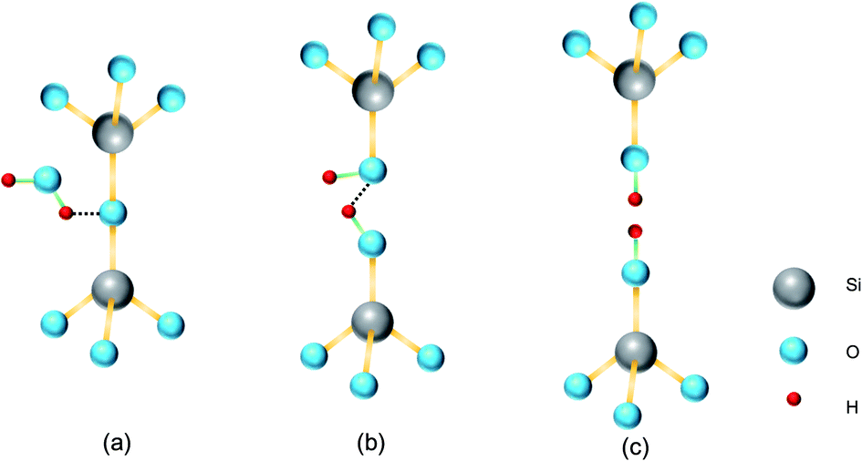 | ||
| Fig. 1 The reaction between water and a strained Si–O–Si bond: (a) adsorption of water molecule to Si–O bond; (b) connection of the generated hydroxyls with the help of hydrogen bonds, and (c) formation of surface hydroxyls. | ||
Recently, it has been reported that surface activation can also be achieved by ultraviolet (UV) cleaning,18,19 which suffers less damage due to the lack of ions bombardment compared with plasma activation.20 And a shorter-wavelength vacuum ultraviolet (VUV) has been found to be more beneficial to bonding due to an ultrathin hydrate layer formed through VUV irradiation.21,22 To date, VUV has been successfully applied to Au/Au direct bonding as well as the heterogeneous bonding of polyether ether ketone (PEEK) and Pt.22,23 However, little research has focused on the VUV assisted bonding of Si/Si and quartz/quartz, and the VUV/O3-activated bonding mechanism has never been explored. Therefore, in this paper, we perform a vacuum ultraviolet/ozone (VUV/O3) direct bonding of Si/Si and quartz/quartz, and study the surface morphology and chemical states at different VUV irradiation time in details. Additionally, VUV/O3 activated low-temperature direct bonding models for Si/Si and quartz/quartz are proposed based on the experimental results, respectively.
2. Experimental
2.1 Materials
(100)-oriented, double-side-polished, 3-in. Si wafers with a thickness of 500 μm were used in the experiments. The quartz glass wafers were double-side-polished, 3-in., fused quartz with a thickness of 400 μm. Both silicon and quartz wafers were diced into 10 × 10 mm2 chips to be the samples. The silicon samples were covered with native oxide layers naturally. All wafers were provided by Shanghai Daheng Optics and Fine Mechanics Co., Ltd.2.2 Bonding procedure
2.3 Characterization
Surface wettability was characterized by a contact angle testing instrument with a side-camera imaging system (OCA 25-HTV, DataPhysics). Surface morphologies of silicon and quartz glass before and after VUV irradiation were observed by an atomic force microscopy (AFM) (Dimension Fastscan, Bruker) in tapping mode. Chemical states of sample surfaces were investigated through Fourier transform infrared spectroscopy (FTIR) (Nicolet iS50, Thermo Fisher Scientific) and Raman scattering spectrometer (Nanofinder, NT-MDT) with a 532 nm excitation source. After bonding, the bonded pairs were glued with jigs, and a pull tensile test was performed by a tensile tester (Instron 5569, Instron) at a speed of 0.5 mm min−1. The bonding interfaces were characterized by transmission electron microscopy (TEM) (Talos F200x, FEI) and energy-dispersive X-ray spectroscopy (EDX).3. Results and discussion
3.1 Chemical effects of VUV irradiation
Firstly, the influence of different VUV irradiation time on the wettability of silicon and quartz glass surfaces was conducted. Fig. 2(a) shows the changes of contact angle as irradiation time increases. Captured contact angle images of silicon and quartz glass are also displayed in Fig. 2(b). The contact angles of the bare silicon and quartz glass were 70.6° and 63.6°, respectively. VUV irradiation led to an extremely hydrophilic surface with water droplets almost spreading the entire silicon or quartz glass sample surfaces after 5 min irradiation. All the contact angles on the silicon and quartz glass surfaces were very small (<2°) after VUV irradiation with 6 min or longer time.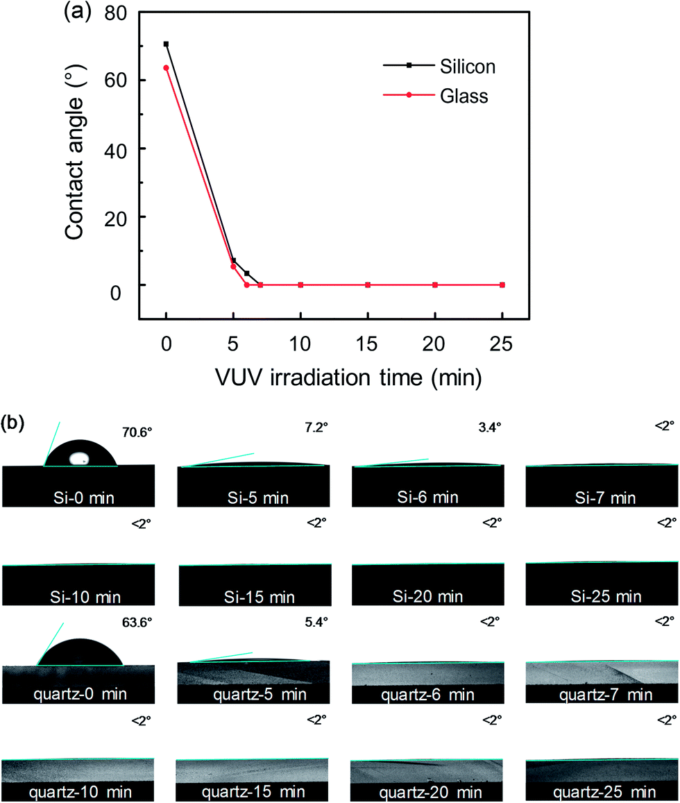 | ||
| Fig. 2 (a) Contact angles of the silicon and the quartz glass surfaces vary with different VUV irradiation time. And the captured contact angle images of silicon and quartz glass are also shown in (b). | ||
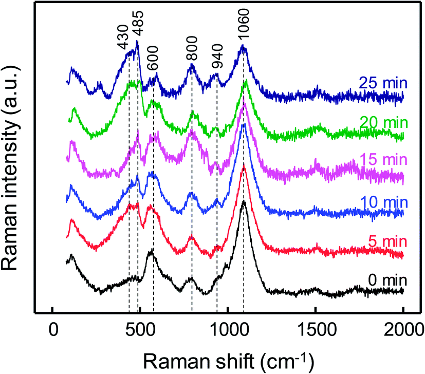
FTIR spectra of silicon and quartz glass are shown in Fig. 3(a) and (b), respectively. Compared with the bare substrates, the absorption band at 3680 cm−1 had a slight increase after 15 min VUV/O3 activation.24,25 And the increased density of silanol group made the surfaces more hydrophilic. To further explore the surfaces of silicon and quartz glass, Raman spectra were used to analyze the changes of surfaces with different VUV irradiation time. Fig. 4 and 5 depict Raman shift of the silicon and the quartz glass with different VUV irradiation time. The peak at 520 cm−1 corresponded to the Si–Si LO peak, which was attributed to the bulk silicon.26 Peaks representing silanol groups (Si–OH) were reported at 940 cm−1 and 980 cm−1.26 The intensities of silanol group dramatically increased after the VUV irradiation. Consequently, surface wettability had been greatly improved as shown in Fig. 2. The peak at 430 cm−1 was assigned to the stretching–bending vibrational modes of Si–O–Si bridges in large silicate rings.27 The ring breathing modes of four- and three-membered silicate rings showed peaks at 485 cm−1 and 600 cm−1, respectively.28 The peak at 800 cm−1 was recognized as the Si–O–Si bending mode. And the peak at approximately 1060 cm−1 was considered to be the asymmetric stretching mode of Si–O–Si bridges in the glass network.29 It was obvious that with the extension of VUV irradiation time, the intensities of peaks at 430 and 485 cm−1 increased, while the intensities of peaks at 800 and 1060 cm−1 decreased. This result can be explained by the break of Si–O–Si bonds in the silicate network caused by the high energy of VUV and the larger rings formed by the newly generated covalent bonds in order to reduce the system energy. Besides, the intensity of the 940 cm−1 peak corresponding to silanol groups was obviously increased after the VUV irradiation.26 The silanol groups on the quartz glass surfaces almost reached saturation after 5 min VUV irradiation according to Fig. 2 and 5.
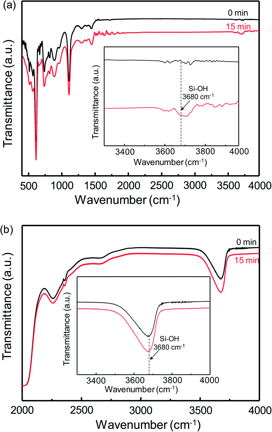 | ||
| Fig. 3 FTIR spectra of (a) silicon and (b) quartz glass surfaces before and after 15 min VUV/O3-activation. | ||
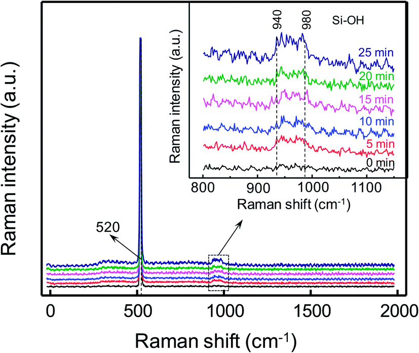 | ||
| Fig. 4 Raman spectra of silicon surfaces with 0, 5, 10, 15, 20 and 25 min VUV irradiation. The inset shows local curves of Raman shifts in 800–1150 cm−1. | ||
 | ||
| Fig. 5 Raman spectra of the quartz glass surfaces with VUV irradiation for 0, 5, 10, 15, 20 and 25 min. | ||
3.2 Physical effects of VUV irradiation
The root-mean-square (RMS) values and surface morphologies of silicon and quartz glass with different VUV irradiation time were investigated by AFM as shown in Fig. 6–8. For silicon, the RMS value slightly increased from 0.301 nm to 0.418 nm with the irradiation time increasing from 0 to 20 min. However, when the irradiation time reached 25 min, the RMS value sharply increased to 0.941 nm. The same trend was also found on the quartz glass surface. AFM height images of silicon and quartz glass were also recorded on 1 × 1 μm2 areas with irradiation time increasing, as presented in Fig. 7 and 8. Both surfaces of silicon and quartz glass generated some asperities with 4–5 nm height after VUV irradiation. Additionally, it was obvious that with the increase of irradiation time, the number of asperities increases, which was attributed to the reason leading to the increase of RMS values.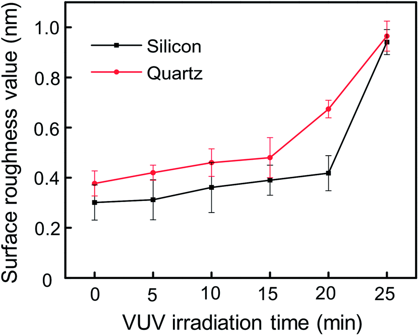 | ||
| Fig. 6 RMS values of silicon and quartz glass surfaces vary with different VUV irradiation time. | ||
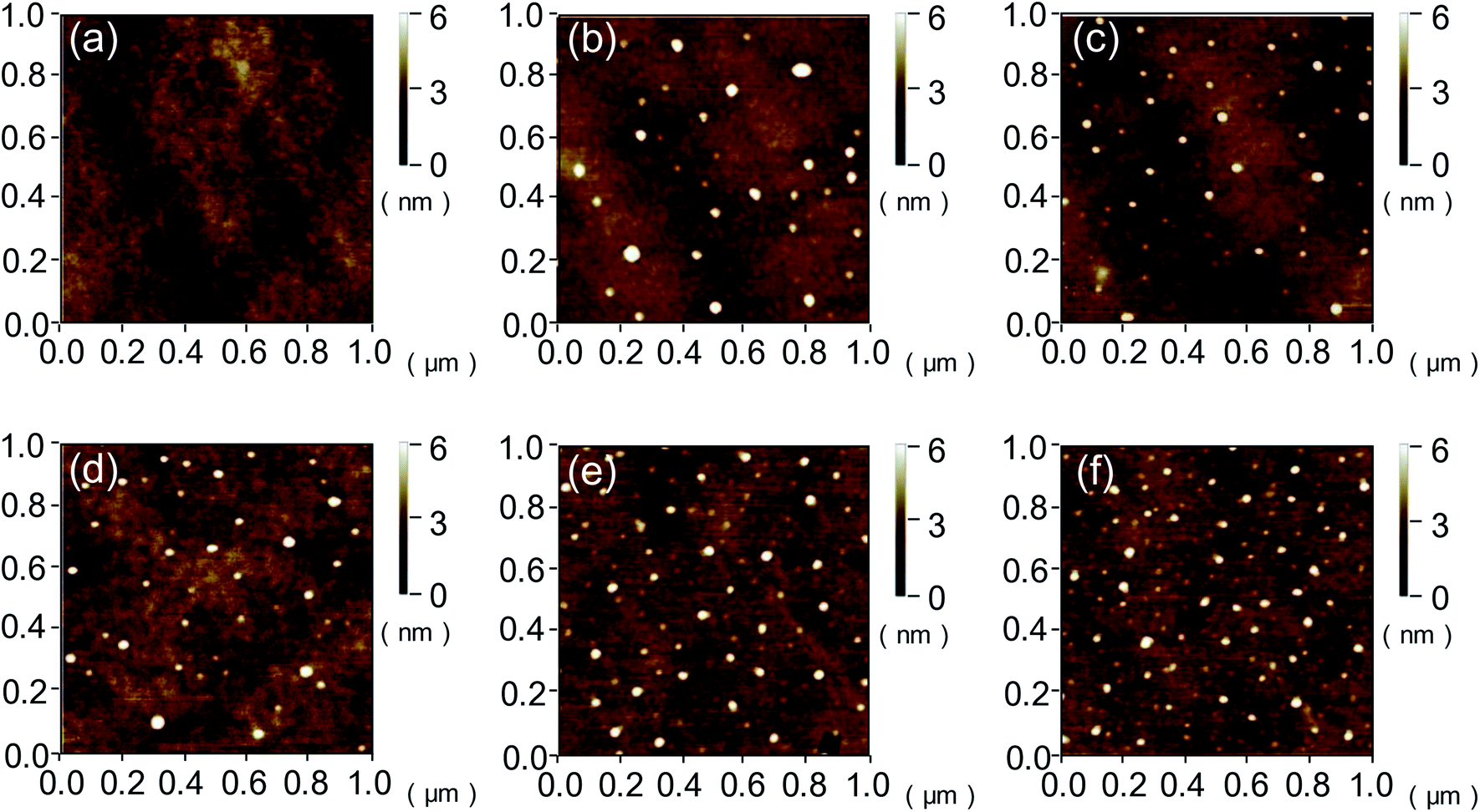 | ||
| Fig. 7 AFM imagines of silicon surfaces with (a) 0, (b) 5, (c) 10, (d) 15, (e) 20 and (f) 25 min VUV irradiation. | ||
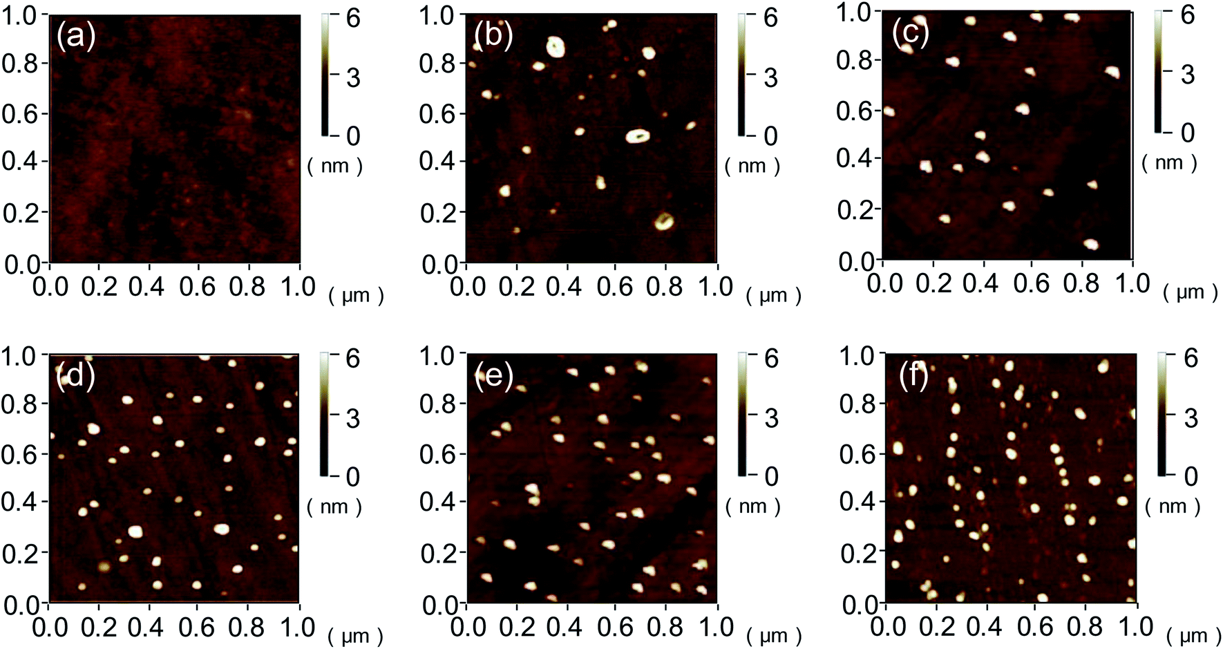 | ||
| Fig. 8 AFM imagines of quartz glass surfaces with (a) 0, (b) 5, (c) 10, (d) 15, (e) 20 and (f) 25 min VUV irradiation. | ||
The energy of VUV rays with a wavelength of 172 nm is 695.49 kJ mol−1,30 while oxygen consists of O![[double bond, length as m-dash]](https://www.rsc.org/images/entities/char_e001.gif) O covalent bonds with a bond energy of 494.4 kJ mol−1.31 Therefore, oxygen in the atmosphere absorbs the VUV radiation and generates highly reactive atomic oxygen. And then the atomic oxygen reacts with molecular oxygen in the air to form O3. Next, atomic oxygen and ozone around the sample surfaces react with organic contaminants and decomposed into harmless volatile H2O, CO2 and NOx. After the contaminants are eliminated, atomic oxygen and ozone begin to interact with silicon and quartz glass surfaces. So there are some asperities corresponding to the silicon oxide grown on the sample surfaces. With longer irradiation time, the amount of asperities increases, and eventually the surface roughness gradually increases. Additionally, although these newly generated asperities cause greater surface roughness, they may have more deformation ability and play an important role in the bonding process. We will further discuss its function in the bonding mechanism section.
O covalent bonds with a bond energy of 494.4 kJ mol−1.31 Therefore, oxygen in the atmosphere absorbs the VUV radiation and generates highly reactive atomic oxygen. And then the atomic oxygen reacts with molecular oxygen in the air to form O3. Next, atomic oxygen and ozone around the sample surfaces react with organic contaminants and decomposed into harmless volatile H2O, CO2 and NOx. After the contaminants are eliminated, atomic oxygen and ozone begin to interact with silicon and quartz glass surfaces. So there are some asperities corresponding to the silicon oxide grown on the sample surfaces. With longer irradiation time, the amount of asperities increases, and eventually the surface roughness gradually increases. Additionally, although these newly generated asperities cause greater surface roughness, they may have more deformation ability and play an important role in the bonding process. We will further discuss its function in the bonding mechanism section.
3.3 Bonding strength and bonding interface
The bonding strengths and pulling strength–displacement curves of Si/Si and quartz/quartz pairs at different annealing temperatures are described in Fig. 9(a) and (b), respectively. It was obvious that the bonding strengths of VUV/O3 activated Si/Si and quartz/quartz pairs are significantly higher than the hydrophilic Si/Si bonding strength at the same annealing temperature. And the bonding strength of VUV/O3 activated Si/Si pairs even at 200 °C annealing temperature (7.13 MPa) is 1.6 times that of conventional Si/Si direct bonding strength (∼4.4 MPa) after annealing at 400 °C.32,33 | ||
| Fig. 9 (a) Bonding strength of Si/Si and quartz/quartz in VUV/O3 activated direct bonding compared with conventional hydrophilic Si/Si bonding strength.32,33 (b) Pulling force–displacement curves of Si/Si and quartz/quartz. | ||
On the other hand, both the Si/Si and the quartz/quartz bonding strengths increased rapidly when the annealing temperature changed from 150 °C to 200 °C, while it grew slowly as the temperature varied from 200 °C to 300 °C. Additionally, the bonding strength of Si/Si pairs was stronger than that of quartz/quartz pairs at any annealing temperatures. Moreover, the phenomena of Si/Si bonded pair was stronger also appeared in the plasma activated bonding. It might be that VUV/O3 made the subsurface of substrates produce an amorphous aquifer layer as a result of plasma influence.15 And this made it possible to obtain higher bonding strength even at low annealing temperatures.
Fig. 10 shows the cross-sectional TEM images and element analysis of the Si/Si and quartz/quartz bonded pairs across the bonding interfaces. For the Si/Si bonded pair, there was a transition layer with thickness estimated to be 20 nm at the interface (Fig. 8(a)). A tight and smooth interface without any microvoids or gaps could also be observed. The transition layer is consisted of three amorphous layers (Fig. 10(a)). Two sides of the interface near the silicon substrate, the content of Si and O elements varied linearly with the distance from the silicon substrate. And the ratio of O/Si raised gradually with the increase of distance. Thickness of this kind of layer was ∼5 nm. In the middle area of the interface, there was a ∼7 nm thickness layers with a stable ratio value of O/Si (∼0.67 as shown in Fig. 10(b)). As mentioned above, ozone and atomic oxygen produced by VUV irradiation have a strong oxidation ability. Thus, there would be a certain thickness of the oxide layer and the degree of oxidation decreased gradually as the distance from the silicon surface increased. In the process of the pre-bonded Si/Si pairs annealed at 200 °C for 8 h, Si and O atoms diffused at the boundary owing to reduce the concentration gradient. So there were three different oxide layers at the bonding interface.
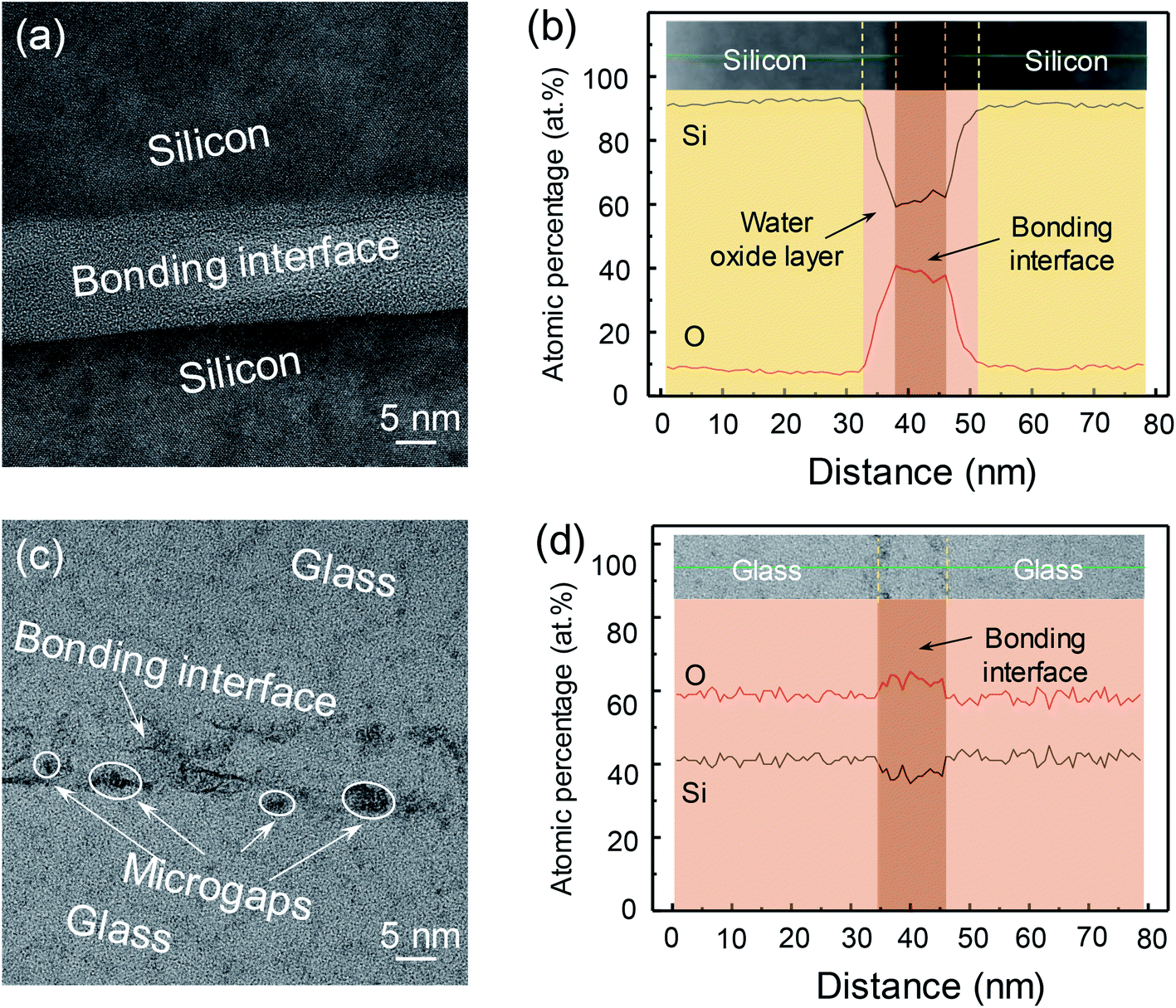 | ||
| Fig. 10 Cross-sectional TEM images of (a) Si/Si and (c) quartz/quartz bonded pairs annealed at 200 °C for 8 h. Elemental analysis of (b) Si/Si and (d) quartz/quartz bonded pairs across the bonding interface with EDS. | ||
For the quartz/quartz bonded pair, there was also a ∼10 nm thickness layer between the quartz glass samples (Fig. 10(c)). But it was different from the Si/Si bonded pairs that the content of transition layer almost unchanged, as shown in Fig. 10(d). Due to quartz glass surfaces were activated by VUV/O3, the content of oxygen in the subsurface is higher than that of bulk quartz glass. Therefore, an oxygen rich interface is formed in the quartz/quartz bonded pairs. Additionally, it is obvious that there are some microgaps at the interface. It was mainly due to the trapped water had little effects on the increase of the interfacial volume. Accordingly, some microgaps were produced after the interfacial water was completely consumed.
3.4 Bonding mechanism
On the basis of our experimental results, influences of VUV on silicon and quartz glass surfaces can be obtained: (1) VUV makes surfaces extremely hydrophilic due to the saturated silanol groups; (2) silicon oxide asperities are formed on the surfaces activated by VUV and O3.| Si–OH + HO–Si → Si–O–Si + H2O | (1) |
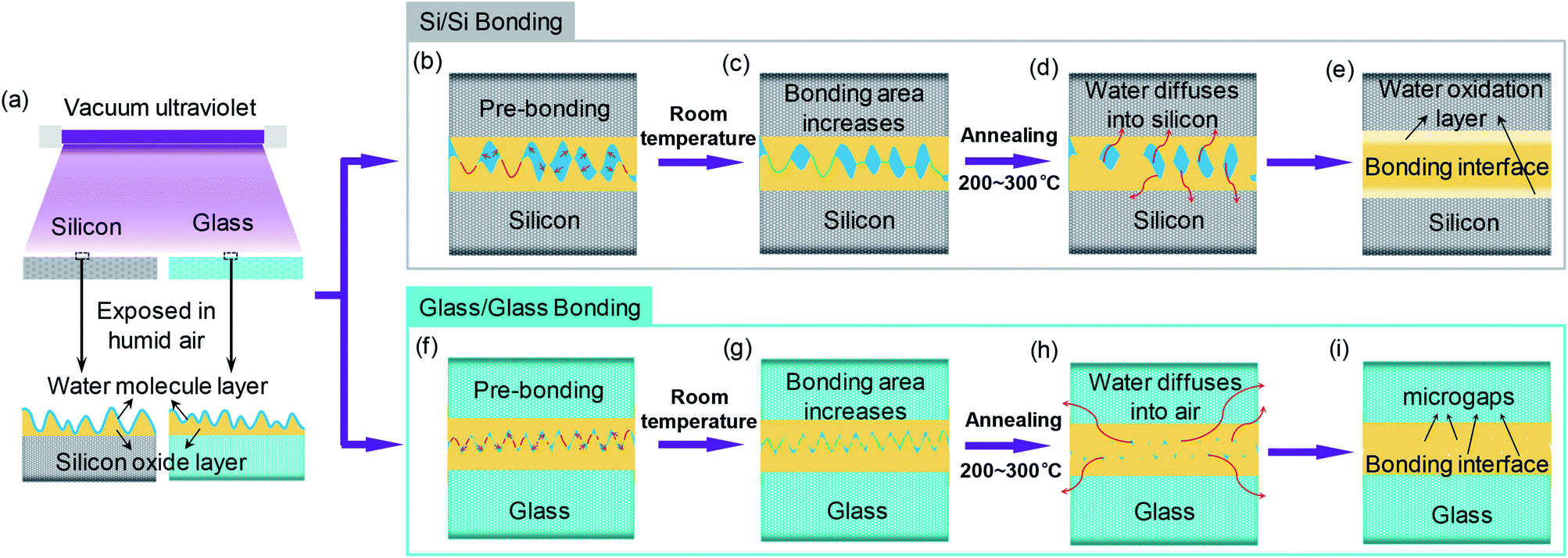 | ||
| Fig. 11 Schematic drawings of the mechanism for low temperature Si/Si and quartz/quartz direct bonding via VUV/O3 activation: (a) VUV-irradiated treatment; (b) Si/Si and (f) quartz/quartz pre-bonding process; WSC makes the (c) Si/Si and (g) quartz/quartz bonding area increases; behaviors of water molecules in the annealing process of (d) Si/Si and (h) quartz/quartz bonded pairs; deformation of the compact (e) Si/Si and (i) quartz/quartz bonding interface. | ||
With the help of hydrogen bonds, linkages of water molecules and silanol groups bridge the gaps between the mating surfaces. Both Fig. 11(b) and (f) depict this initial pre-bonding process, the red lines represent the covalent bond formation regions. As previously described, the trapped water at the bonding interface may induce the WSC, which would soften the silicon or quartz glass surfaces close to water molecules, promoting the increase of bonding area (the green lines in Fig. 10(c) and (g) represent the increased bonding area). However, it is worth noting that the bonding strength is still very low (<1 kPa) because the hydrogen bonds play a major role in Si/Si or quartz/quartz pre-bonded pairs.
| Si + 2H2O → SiO2 + 2H2 | (2) |
For the molar volume of silicon dioxide is larger than that of silicon, this oxidation process may increase the deformation of asperities, thereby facilitating the gap closure. With the increase of the distance between bonding interfaces, the oxidation of water oxidation layer gradually decreases. Therefore, a bonding interface of three layers is formed as shown in Fig. 10(a), (b) and (e).
For the quartz/quartz bonding, there is no oxidation reaction between water and quartz glass substrate. Therefore, the volume of silicon oxide remains unchanged at the interface and the mating surfaces cannot expand to each other. The interfacial water molecules tend to volatilize into air during the annealing process as shown in Fig. 11(h). However, the diffusion of interfacial atoms is difficult to make the gap closure. Discontinuous boundaries will be formed when the interfacial water disappears (Fig. 11(i)).
4. Conclusions
Low-temperature direct bonding of Si/Si and quartz/quartz was achieved via VUV/O3 activation. No UHV environment or extra force was applied in the bonding process. The bonding strength of Si/Si and quartz/quartz pairs reached up to 6.95 MPa and 6.14 MPa respectively after annealing at 200 °C. Additionally, a bonding model comprising WSC and asperity deformation was proposed based on the experimental results. After VUV irradiation, both silicon and quartz glass surfaces became very hydrophilic due to the saturated silanol groups, which can be confirmed by Raman spectra. Although it had been observed in the AFM images that the oxide asperities might increase the surface roughness, their strong deformability owing to WSC would be beneficial to gap closure. In the Si/Si bonded pairs, a tight interface consisting of three oxide layers was obtained due to the water oxidation during annealing procedure. However, water had less effect on the volume increase of interfaces, and microgaps were eventually formed in the quartz/quartz bonded pairs.Conflicts of interest
There are no conflicts to declare.Acknowledgements
This work was supported by the National Natural Science Foundation of China (Grant No. 51505106), the China Postdoctoral Science Foundation (Grant No. 2017M610207), and the Heilongjiang Postdoctoral Foundation (No. LBH-Z16074).References
- J. B. Lasky, Appl. Phys. Lett., 1986, 48, 78–80 CrossRef CAS.
- S. H. Christiansen, R. Singh and U. Gösele, Proc. IEEE, 2006, 94, 2060–2106 CrossRef CAS.
- K. Mawatari, Y. Kazoe, H. Shimizu, Y. Pihosh and T. Kitamori, Anal. Chem., 2014, 86, 4068–4077 CrossRef CAS PubMed.
- M. Shimbo, K. Furukawa, K. Fukuda and K. Tanzawa, J. Appl. Phys., 1986, 60, 2987–2989 CrossRef CAS.
- Q. Y. Tong, G. Cha, R. Gafiteanu and U. Gosele, J. Microelectromech. Syst., 1994, 3, 29–35 CrossRef CAS.
- C. Mai, M. Li and S. Yang, RSC Adv., 2015, 5, 42721–42727 RSC.
- U. Gösele, H. Stenzel, T. Martini, J. Steinkirchner, D. Conrad and K. Scheerschmidt, Appl. Phys. Lett., 1995, 67, 3614–3616 CrossRef.
- M. M. R. Howlader, S. Suehara and T. Suga, Sens. Actuators, A, 2006, 127, 31–36 CrossRef CAS.
- A. U. Alam, M. M. R. Howlader and M. J. Deen, ECS J. Solid State Sci. Technol., 2013, 2, P515–P523 CrossRef CAS.
- U. I. Can and B. Bayram, Diamond Relat. Mater., 2014, 47, 53–57 CrossRef CAS.
- C. Wang, Y. Liu and T. Suga, ECS J. Solid State Sci. Technol., 2017, 6, 7–13 CrossRef.
- M. M. R. Howlader, F. Zhang and M. G. Kibria, J. Micromech. Microeng., 2010, 20, 65012 CrossRef.
- Q. Y. Tong, J. Electrochem. Soc., 1996, 143, 1773 CrossRef CAS.
- V. Masteika, J. Kowal, N. S. J. Braithwaite and T. Rogers, ECS J. Solid State Sci. Technol., 2014, 3, Q42–Q54 CrossRef CAS.
- T. Plach, K. Hingerl, S. Tollabimazraehno, G. Hesser, V. Dragoi and M. Wimplinger, J. Appl. Phys., 2013, 113, 94905 CrossRef.
- T. A. Michalske and S. W. Freiman, Nature, 1982, 295, 511–512 CrossRef CAS.
- T. A. Michalske and S. W. Freiman, J. Am. Ceram. Soc., 1983, 66, 284–288 CrossRef CAS.
- T. Takahagi, I. Nagai, A. Ishitani and H. Kuroda, J. Appl. Phys., 1988, 64, 3516–3521 CrossRef CAS.
- J. Fan, G. Y. Chong and C. S. Tan, ECS J. Solid State Sci. Technol., 2012, 1, 291–296 CrossRef.
- B. Ma, H. Kuwae, A. Okada, W. Fu, S. Shoji and J. Mizuno, in 2016 International Conference on Electronics Packaging (ICEP), IEEE, 2016, pp. 447–450 Search PubMed.
- C. Wang, J. Xu, X. Qi, Y. Liu, Y. Tian, C. Wang and T. Suga, J. Electrochem. Soc., 2018, 165, H3093–H3098 CrossRef.
- W. Fu, A. Shigetou, S. Shoji and J. Mizuno, Mater. Sci. Eng., C, 2017, 79, 860–865 CrossRef CAS PubMed.
- A. Okada, S. Shoji, M. Nimura, A. Shigetou, K. Sakuma and J. Mizuno, Mater. Trans., 2013, 54, 2139–2143 CrossRef CAS.
- F. Rubio, J. Rubio and J. L. Oteo, Spectrosc. Lett., 1998, 31, 199–219 CrossRef CAS.
- J. A. Theil, D. V. Tsu, M. W. Watkins, S. S. Kim and G. Lucovsky, J. Vac. Sci. Technol., A, 1990, 8, 1374–1381 CAS.
- S. Agnello, D. Di Francesca, A. Alessi, G. Iovino, M. Cannas, S. Girard, A. Boukenter and Y. Ouerdane, J. Appl. Phys., 2013, 114, 104305 CrossRef.
- G. E. Walrafen and P. N. Krishnan, J. Chem. Phys., 1981, 74, 5328–5330 CrossRef CAS.
- A. Pasquarello and R. Car, Phys. Rev. Lett., 1998, 80, 5145–5147 CrossRef CAS.
- A. Winterstein-Beckmann, D. Möncke, D. Palles, E. I. Kamitsos and L. Wondraczek, J. Non-Cryst. Solids, 2014, 401, 110–114 CrossRef CAS.
- R. A. Barb, B. Magnus, S. Innerbichler, T. Greunz, M. Wiesbauer, R. Marksteiner, D. Stifter and J. Heitz, Appl. Surf. Sci., 2015, 325, 105–111 CrossRef CAS.
- J. Berkowitz, G. B. Ellison and D. Gutman, J. Phys. Chem., 1994, 98, 2744–2765 CrossRef CAS.
- M. Shimbo, K. Furukawa, K. Fukuda and K. Tanzawa, J. Appl. Phys., 1986, 60, 2987–2989 CrossRef CAS.
- M. M. R. Howlader, F. Zhang and M. J. Kim, J. Microelectromech. Syst., 2011, 20, 17–20 CrossRef.
- C. Wang, Y. Wang, Y. Tian, C. Wang and T. Suga, Appl. Phys. Lett., 2017, 110, 221602 CrossRef.
- S. Vincent, I. Radu, D. Landru, F. Letertre and F. Rieutord, Appl. Phys. Lett., 2009, 94, 101914 CrossRef.
| This journal is © The Royal Society of Chemistry 2018 |