
 Open Access Article
 This Open Access Article is licensed under a Creative Commons Attribution-Non Commercial 3.0 Unported Licence
Significantly enhanced dielectric and hydrophobic properties of SiO2@MgO/PMMA composite films
Yuting Xia,
Jiayun Chen,
Zhicai Zhu,
Qilong Zhang *,
Hui Yang and
Qianqian Wang
*,
Hui Yang and
Qianqian Wang
School of Materials Science and Engineering, State Key Lab Silicon Mat, Zhejiang University, Hangzhou 310027, PR China. E-mail: mse237@zju.edu.cn
First published on 23rd January 2018
Abstract
In this article, we provide a feasible method to prepare high-dielectric-constant hydrophobic composite films, which show potential application as the insulator layer in electrowetting devices. SiO2@MgO core–shell nanoparticles were fabricated via a hydrolysis process and embedded into the PMMA matrix. The microstructure of the nanoparticles and the cross-section of the films indicated that a SiO2 coating has successfully been prepared around the MgO particles with a thickness of about 20–30 nm and the nanofillers were homogeneously dispersed in the polymer. Hydrophobic films (contact angle ∼115°) with appropriate glass transition temperature were obtained. The dielectric constant at various frequencies of the functional fillers enhanced with increasing the SiO2@MgO filler content. The results suggested that SiO2@MgO is more effective in increasing the dielectric constant of PMMA when compared with MgO sheets. Typically, the dielectric constant of the PMMA composite filled with 40 wt% SiO2@MgO reaches 19.1 at 40 Hz, in contrast to 9.7 for the composite filled with 40 wt% MgO sheets and 3.8 for pristine PMMA. Also, the composites exhibited low electrical conductivity (≤10−7) even at high frequency. All the improved performances showed potential application in the dielectric layer of electrowetting devices.
Introduction
Electrowetting-on-dielectric is a small-scale liquid handling technology that has been significantly used for numerous applications, including electronic displays, optical devices, lab on a chip, liquid transport in microfluidic devices, and surface science.1–4 In recent years, the electrowetting display has been widely investigated and plays an important role in the field of display devices, combining the special reflective display characteristics of conventional printed paper with the changeable electronic information.2–5 Fig. 1 shows the principle of electrowetting, based on the voltage-controlled transformation of a coloured oil drop contrast to a white substrate.9 The applied voltage changed the electrical potential between the ITO electrode and the coloured drop, increasing the charge density in the interface and resulting in a wetting and flattening variation of the oil droplet. The relationship between the applied voltage and change of contact angle at the solid–liquid interface can be described by the Young–Lippmann equation:3,6
 | (1) |
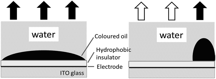 | ||
| Fig. 1 The principle of electrowetting display. | ||
Dielectric layer is one of the vital sections in electrowetting display device, the materials selection and preparation of dielectric layer can directly influence the performance and application of the device. According to the eqn (1), the film should provide some special properties for the electrowetting display devices except for insulation. First, the surface should be hydrophobic to ensure a huge variation in contact angle under electrical field. Second, the film should have a comparatively small threshold voltage because a high actuation voltage may cause electrolysis of the droplet or the breakdown of film. The threshold voltage was related to the dielectric permittivity and thickness of insulating layer. While in most situations, ultra-thin insulators increased the contact angle range at the expense of electrical breakdown and even failed before the contact angle varied large enough.7,8 So, a film with high permittivity and hydrophobic properties is essential.
In general, dielectric material can be divided into two categories: polymer and ceramics. Polymers, such as amorphous fluoropolymer,13 PDMS,9,10 PI,11,12 parylene-C,11 parylene-N13 and parylene-HT,14 offer the superiorities in hydrophobic properties, economy, low temperature processing and shape and large area preparation. But most of the dielectric constant value of hydrophobic polymer is less than 3, requiring high actuation voltage. For example, Teflon AF1600 (ref. 15 and 16) is a typical fluoropolymer used in electrowetting devices with a high contact angle (∼120°), while the applied voltage of devices is up 80 volts, owing to the low dielectric constant ε of Teflon AF1600 (1.93). However, common ceramic materials, such as SiO2 (ref. 17 and 18) (ε ∼ 4), (Ba, Sr)TiO3 (ref. 19) (BST, ε ∼ 180), Ta2O5 (ref. 20–22) (ε = 20–25), Si3N4 (ref. 23 and 24) (ε ∼ 8), and Al2O3 (ref. 24–26) (ε ∼ 10) have relatively high dielectric constant do not provide good hydrophobic property. Also in the preparation section, some special techniques like chemical vapor deposition (CVD), atomic layer deposition (ALD) and sputtering are required to deposit uniform oxide dielectrics, which are always along with high temperature. To reduce the actuation voltage, many researchers covered a thin layer of hydrophobic polymer on the high dielectric film to ensure a high contact angle. Bilayer structures such as Al2O3-Cytop,12 P (VDF-HFP)-Teflon AF,32 SiO2/Si3N4-Cytop,24 AF1600/Si3N4/TiO2 (ref. 27) and Teflon-AF/CYTOP/Ta2O5 (ref. 33) are used to control the movement of droplet. But this structure design makes the fabrication process complex, which increased the manufacturing cost.
In this work, PMMA34 was chosen as polymer matrix; SiO2@MgO core–shell nanostructure was constructed and embedded into the PMMA for preparing the single-layer dielectric film with high permittivity and hydrophobic properties. In this structure, MgO nanofillers possesses a relatively high permittivity (ε ∼ 10), which are imposed to increase the dielectric constant of PMMA. Furthermore, the permittivity contrast between the inorganic filler and the polymer matrix always lead to inhomogeneous distribution of the electric fields, which may deteriorate the systematic dielectric properties. For this reason, SiO2 (ε ∼ 4) wrapped the MgO as interlayer between the fillers and the matrix and also protect MgO powders from hydrolysis and other physicochemical changes. Firstly, the MgO nanosheets were prepared via a hydrothermal process with an average thickness of 25 nm. Secondly, the surface-coated MgO nanosheets with a SiO2 layer were synthesized by a simple hydrolysis process at ambient temperature. Lastly, a single-layer dielectric film is obtained by solution mixture and tape-casting process. A systematic study concerning the influence of nanofillers on dielectric properties, glass transition temperature, conductivity and contact angle of PMMA composites is showed. Commercial MgO-filled composites are also prepared to demonstrate the impact of nanofillers. The obtained SiO2@MgO/PMMA composites film exhibited high dielectric constant and hydrophobic properties, which has potential value in electrowetting devices.
Results and discussion
Fig. 2(a) shows the XRD patterns of the MgO nanosheets and the SiO2@MgO shell@core nanoparticles. The diffraction peaks of the (1 1 1), (2 0 0), and (2 2 0) planes can be indexed to the cubic (Fm3m) MgO (JCPDS 45-0946). For SiO2@MgO nanoparticles, there was no obvious characteristic peak of SiO2 phase observed in the pattern, indicating that SiO2 might exist as amorphous phases or has low crystallinity compared with the MgO nanoparticles. And MgO nanosheets show higher intensity of MgO characteristic peaks. To further confirm the composition of the coating, Fig. 2(b) compared the XPS survey spectrum of MgO and SiO2@MgO. Both of the two samples contain mainly Mg, O and C elements, and the observed C emission peak may be caused by the transfer process of samples into the UHV chamber.28,29 An apparent Si emission peak was observed in the XPS spectrum of SiO2@MgO powders, demonstrating the existence of SiO2. The core–shell structure will be confirmed by morphology of samples.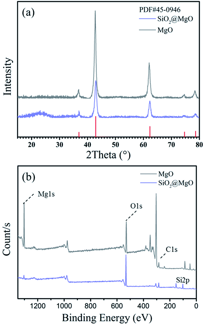 | ||
| Fig. 2 (a) XRD patterns and (b) XPS of MgO nanosheets and SiO2@MgO powders. | ||
Fig. 3(a) and (b) show the typical morphology of the 2D petal-like MgO nanosheets with diameters from 0.5 to 1 μm. Detailed observations reveal that surface of MgO was not very flat and nanosheets are estimated by AFM to be around 25 nm in thickness. Fig. 3(c) shows that slightly grooves exist on the surface and induce lager surface area (131.5 m g−1). The microstructure of coating is shown in Fig. 3(d). It can be clearly seen that the core–shell structure and the coverage of the coating is at a high level with fine layered features. The insert picture shows that thickness of the coating layer is about 25–30 nm.
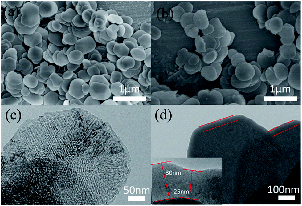 | ||
| Fig. 3 (a and b) SEM and (c) TEM images of MgO nanosheets; (d) TEM images of core–shell structure of SiO2@MgO. | ||
Composite films with different kinds and fractions of fillers were prepared by the solution blending process described in the experimental section. And the thickness of all the films is 40–60 μm measured by the micrometer caliper. Fig. 4 presents the XRD patterns of SiO2@MgO nanoparticles, pure PMMA and SiO2@MgO–PMMA composited with different weight fractions of SiO2@MgO. PMMA is an amorphous polymer and no clearly diffraction peaks can be observed. In the XRD patterns of the composite films, diffraction peaks from MgO and the curve bread from PMMA can be observed. With an increase of MgO content, the X-ray powder diffraction peak curve bread decreases gradually, which means MgO exert a dominant effect on the crystallization behaviour of the nanocomposites.
 | ||
| Fig. 4 XRD patterns of SiO2@MgO particles, pure PMMA and SiO2@MgO–PMMA composites with different weight fractions of SiO2@MgO. | ||
The SEM images of the freeze-fractured cross-sections of MgO–PMMA and SiO2@MgO–PMMA composite films at 40 wt% concentration and pure PMMA film are shown in Fig. 5. Due to the surface effect of nanoscale particle, powders prepared by wet process can form aggregation easily during the desiccation period. The aggregation of MgO sheets were obviously observed in Fig. 5(b). After the ultraphonic and stirring process MgO nanopowders can be easily homodispersed in ethanol and a coating of uniform shell can prevent once more aggregation. Compared with MgO–PMMA, SiO2@MgO powders are homogenously dispersed in the matrix and few voids could be observed between the particles and the polymer (Fig. 5(a)). The phenomenon suggests that SiO2 coating layer can protect MgO from agglomeration during the preparation process, which is also beneficial to the dielectric properties of the composites.30 Ke et al. also prepared core–shell structured BaTiO3/SiO2 to increase the isolation of BaTiO3 nanoparticles.31 Fig. 5(d) shows the element surface distribution in the cross-section of SiO2@MgO–PMMA composite films by the energy spectrum, which also proves the homogenously distribution of fillers.
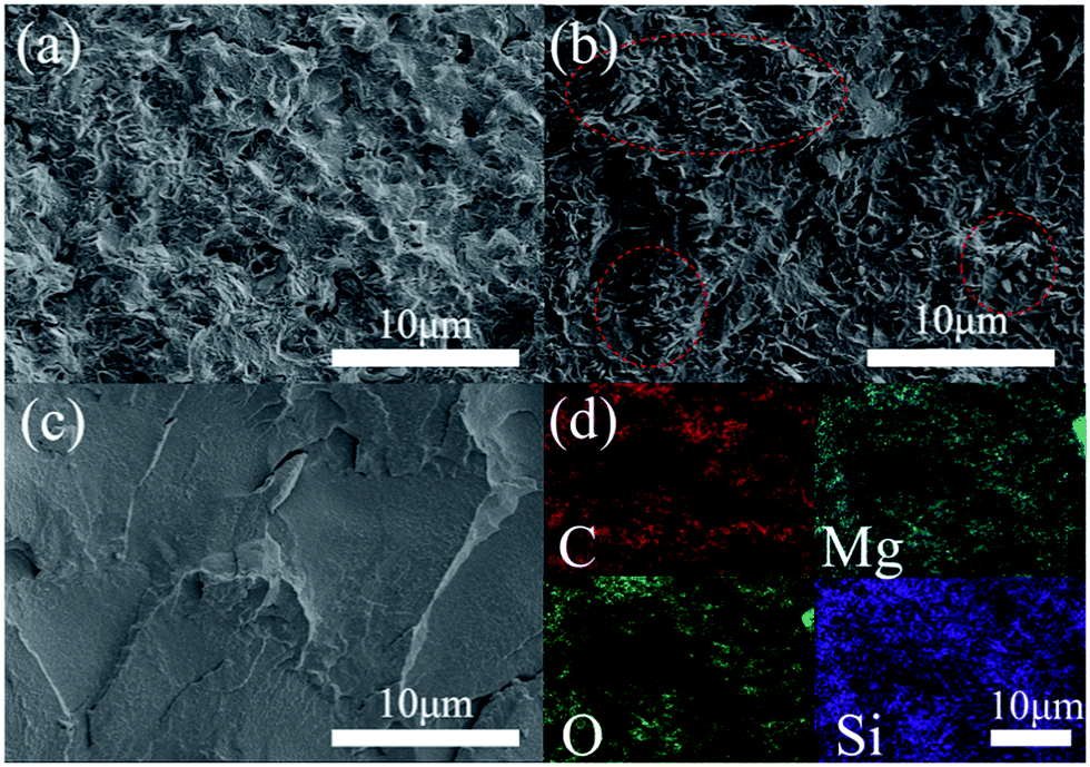 | ||
| Fig. 5 Freeze-fractured cross-sections of (a) 40 wt% SiO2@MgO–PMMA, (b) 40 wt% MgO–PMMA and (c) PMMA films. (d) Element distribution of (a). | ||
The glass transition temperature of PMMA and its nanocomposites with different filler loadings has been showed in Fig. 6. It is apparent that the addition of fillers leads to an increase in the Tg. With an increase of SiO2@MgO loading, Tg increases. But the MgO and SiO2 are ceramic particles, which do not directly contribute to the Tg of the matrix. The possible explanation of this phenomenon is the interfacial effect. The interaction of polymer segments surrounding the particles can alter the segment kinetics in the religion drastically due to the presence of the interface and the importing of particles enhanced the interface area in the system. In this study, PMMA absorbing or grafting onto the SiO2 surface decreases molecular mobility, changes the density of packing of polymer segments, modifies the chain conformation and orientation in the neighbourhood of the surface, and produces a higher glass transition temperature. A similar result of glass transition temperature has also been reported for silica,32 ZnS,33 aluminum,34 and vapour-grown carbon fiber,35 etc. The highest Tg (119.1 °C, 40 wt%) of SiO2@MgO composites is lower than 120 °C, and can be used as further process as a hydrophobic insulator layer of electrowetting display.
 | ||
| Fig. 6 Glass transition temperature of PMMA and its nano-composites with different filler loadings. | ||
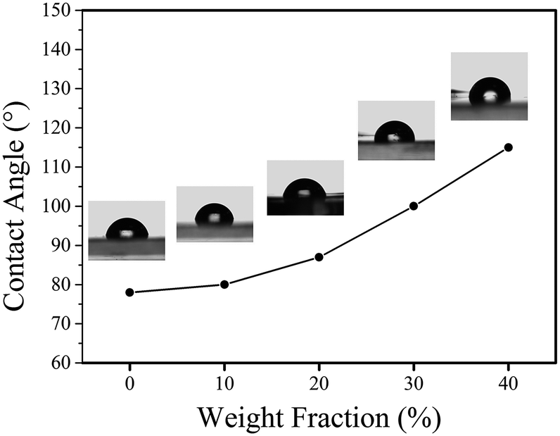
By varying the weight fraction of nanofillers blended with PMMA, we can systematically change the contact angle of the insulator, as shown in Fig. 7. The Young's contact angle increased to about 115°, compared to the pure PMMA (θ ∼ 78°). And the Young's contact angle increased as the increasing of the weight fraction of SiO2@MgO, which is also founded in the BaTiO3–fluoropolymer nanocomposite.36 The increase of contact angle showed the change of surface energy γSV, which was caused by the nanofillers. The chain conformation and orientation of polymer around the fillers has changed and even influenced the chain structure near the film surface with increasing fillers. Also, some inevitable surface particles also contributed to the result. A large initial contact angle provides the possibility for a lager range of dynamic contact angle, shown by the Young–Lippmann equation.
 | ||
| Fig. 7 Contact angles of PMMA and its nanocomposites with different filler loadings. | ||
Fig. 8(a–c) presents the frequency dependence of room temperature dielectric constant (ε), dielectric loss tangent (tan![[thin space (1/6-em)]](https://www.rsc.org/images/entities/char_2009.gif) δ) and electrical conductivity (σ) for the PMMA and its nanocomposites with varied filler weight fractions. For comparison, the properties of composite filled with 40 wt% MgO nanosheets and commercial MgO (c-MgO) are also included. As shown in Fig. 8a, the dielectric constant declines with increasing frequency for all samples in low-frequency region and shows a stronger frequency dependence with increasing SiO2@MgO content over the whole frequency range. At higher frequencies (>103), the variation trend of ε becomes relatively stable. The dielectric constant increased with increasing SiO2@MgO content. The frequency variation tendency shows the typical characteristic of interface polarization.37 The dielectric constant of PMMA composite with 40 wt% SiO2@MgO reaches 19.1 at 40 Hz, in contrasted to 9.7 and 6.8 for the composite with 40 wt% MgO nanosheets and c-MgO, and is nearly 5 times that of pure PMMA (3.8). It should be noted that the dielectric constant of SiO2 and MgO are 3.9 and 10, respectively, which are lower than 19.1. The results of dielectric constant indicate that SiO2 coating has a dramatic effect on the dielectric constant of the nanocomposite.31 In contrast to the expectation, the ε of the core–shell nanocomposite was also higher than the dielectric constant of the nanocomposite with pure MgO. First, the contrast between the MgO and the PMMA may induce the electric field concentration in the polymer38 and SiO2 acts as a medium layer between matrix and MgO for homogeneous electric field. Pan et al. constructed multilayer hierarchical interfaces and used simulation of finite element to demonstrate the effect of core–shell structure.39 Second, the amorphous insulation coating layer could effectively contribute to the mobility of free electrons.39 Third, the coating MgO with amorphous SiO2 can reduce the mismatch with amorphous PMMA avoiding agglomeration, air voids and other defects.40 The frequency dependence behavior shows the typical characteristic of Maxwell–Wagner–Sillars (MWS) interface polarization, which can make contributions at low-frequency range. The three multiple materials increase interface area and enhance interface polarization.41 The charge carriers have enough relaxation time to accumulate at the interfaces between two dielectric media, increasing the dielectric loss and dielectric constant of the nanocomposites with a higher amount of nanoparticles and at lower frequencies.
δ) and electrical conductivity (σ) for the PMMA and its nanocomposites with varied filler weight fractions. For comparison, the properties of composite filled with 40 wt% MgO nanosheets and commercial MgO (c-MgO) are also included. As shown in Fig. 8a, the dielectric constant declines with increasing frequency for all samples in low-frequency region and shows a stronger frequency dependence with increasing SiO2@MgO content over the whole frequency range. At higher frequencies (>103), the variation trend of ε becomes relatively stable. The dielectric constant increased with increasing SiO2@MgO content. The frequency variation tendency shows the typical characteristic of interface polarization.37 The dielectric constant of PMMA composite with 40 wt% SiO2@MgO reaches 19.1 at 40 Hz, in contrasted to 9.7 and 6.8 for the composite with 40 wt% MgO nanosheets and c-MgO, and is nearly 5 times that of pure PMMA (3.8). It should be noted that the dielectric constant of SiO2 and MgO are 3.9 and 10, respectively, which are lower than 19.1. The results of dielectric constant indicate that SiO2 coating has a dramatic effect on the dielectric constant of the nanocomposite.31 In contrast to the expectation, the ε of the core–shell nanocomposite was also higher than the dielectric constant of the nanocomposite with pure MgO. First, the contrast between the MgO and the PMMA may induce the electric field concentration in the polymer38 and SiO2 acts as a medium layer between matrix and MgO for homogeneous electric field. Pan et al. constructed multilayer hierarchical interfaces and used simulation of finite element to demonstrate the effect of core–shell structure.39 Second, the amorphous insulation coating layer could effectively contribute to the mobility of free electrons.39 Third, the coating MgO with amorphous SiO2 can reduce the mismatch with amorphous PMMA avoiding agglomeration, air voids and other defects.40 The frequency dependence behavior shows the typical characteristic of Maxwell–Wagner–Sillars (MWS) interface polarization, which can make contributions at low-frequency range. The three multiple materials increase interface area and enhance interface polarization.41 The charge carriers have enough relaxation time to accumulate at the interfaces between two dielectric media, increasing the dielectric loss and dielectric constant of the nanocomposites with a higher amount of nanoparticles and at lower frequencies.
 | ||
| Fig. 8 Frequency dependence of (a) dielectric constant, (b) dielectric loss and (c) conductivity of PMMA, MgO–PMMA and SiO2@MgO–PMMA composites with different weight ratios. | ||
The dielectric loss tangent of all samples also shows strong frequency dependence in Fig. 8(b). Under the frequency for 40 to 106 Hz, the dielectric loss tangent drastically decreases with the increasing frequency and enhances with core–shell nanocomposits content. The trend could be explained by the accumulation of extra sources of space charge carriers induced by inorganic fillers.42
Fig. 8(c) shows the electric conductivity for the nanocomposites increases with the increasing frequency and is only slightly higher than that of pure PMMA over the whole frequency range. The slight increase could be explained by the interface induced by the nanofillers where charge carriers easily accumulated and the same result also existed in other ref. 43 and 44. The electric conductivity of all samples over the frequency from 102 to 106 is lower than 10−7 S cm−1, indicating the excellent insulation of the films. The good insulating properties may be attributed to the insulating core–shell nanoparticles and the homogeneous dispersion in the polymer matrix.
Dielectric breakdown strength (BDS) is also an important property of the nanocomposites determining the applied electric filed away from breakdown. The characteristic BDS is a statistic value and analyzed by a two-parameter Weibull distribution function, described as:45,46

 | ||
| Fig. 9 Weibull plots of the breakdown strength for MgO–PMMA and SiO2@MgO–PMMA composites. | ||
| Sample | SiO2@MgO | MgO | c-MgO | |||
|---|---|---|---|---|---|---|
| 10 wt% | 20 wt% | 30 wt% | 40 wt% | 40 wt% | 40 wt% | |
| Eb | 167 | 152 | 116 | 101 | 119 | 98 |
| β | 14.46 | 7.77 | 12.96 | 5.16 | 4.90 | 4.23 |
Conclusions
In summary, core–shell structure SiO2@MgO particles have been successfully fabricated by a hydrolysis process as functional fillers and MgO nanosheets have been prepared via a facile hydrothermal process. Microstructure analyses indicated that SiO2@MgO particles homogeneously dispersed in PMMA matrix. Hydrophobic film (contact angle ∼ 115°) with appropriate glass transition temperature was obtained. Compared with commercial MgO-filled composites, the frequency dependent dielectric properties of the functional fillers showed much greater increase (about 300%), while presented similar breakdown strength (over 100 MV m−1). Especially, all the composites exhibited low electric conductivity (≤10−7) even at high frequency. Our work could provide a feasible method to prepare high-dielectric-constant insulator layer with hydrophobic properties in electrowetting devices.Experimental
Materials
Magnesium chloride hexahydrate (MgCl2·6H2O), polyvinyl pyrrolidone (PVP, K30), N,N-dimethylformamide (DMF) and magnesium oxide (MgO, <50 nm, 99.9% metal basis) were purchased from Aladdin Industrial Corporation. Tetraethyl orthosilicate (TEOS), ethanol and ammonia solution (30 wt%) were supplied by Sinopharm Chemical Reagent Co. Ltd., China. The poly(methyl methacrylate) (PMMA) was provided by Sigma-Aldrich with average molecular weight about 120000 by GPC. All chemicals were used as received without any further treatment.
Synthesis of MgO nanosheets
The MgO nanosheets were prepared by a single step hydrothermal approach. In a typical procedure, 20 mmol MgCl2·6H2O and 1 g PVP was add into 65 mL deionized water containing 3 mL ammonia. After stirring for 30 min at room temperature, the solution was transferred into a 100 mL Teflon-lined stainless steel autoclave and heated to 180 °C and maintained for 3 hours. Then the precipitates were washed with ethanol and deionized water for several times and dried at 60 °C for 12 h. Finally, the as-synthesized white powders were calcined in air at 500 °C for 3 h and harvested for subsequent preparation.Synthesis of SiO2@MgO core–shell nanoparticles
SiO2@MgO powders were prepared by a hydrolysis method, 1 g as-prepared MgO nanosheets were add to 70 mL ethanol. After ultrasonic dispersion for 20 min, 1.5 mL ammonia solution in 4 mL deionized water and 0.8 mL TEOS in 20 mL ethanol were consecutively added. And the mixture was continuous stirred for 6 hours at the room temperature. The products were separated out and washed only by ethanol for several times, and then dried at 60 °C under vacuum condition.Preparation of PMMA composites
PMMA particles were first dissolved in DMF, and stirred for 4 hours to get a homogeneous solution. Then a certain amount of prepared SiO2@MgO particles were added into the solution and sonicated in an ultrasonic washer for 1 h. After vigorously stirring at room temperature for 24 h, the homogeneous mixture was put into vacuum container for 1 h to discharge bubbles. The mixture was poured onto a clean glass plate and shaped by casting equipment (MSK-AFA-III, HEFEI Ke Jing Materials Technology Co., Ltd.). The film was dried in a vacuum oven at 60 °C for 12 h to remove the residual DMF. Pure PMMA and MgO–PMMA films were also prepared with same method as comparison.Characterization
The X-ray diffraction patterns of the products were evaluated with Cu Kα radiation (XRD, EMPYREAN, PANalytical Co., The Netherlands). The chemical composition of the products was identified by the ESCALAB 250XI X-ray photoelectron spectrometer (XPS, Thermo Fisher Scientific, USA). The morphology of products were observed by a field emission scanning electron microscopy (FESEM, S-4800, Hitachi Ltd, Japan) and a transmission electron microscopy (TEM, Tecnai G2 F20, FEI Co., Netherlands) with an accelerating voltage of 200 kV. The surface area of MgO sheets were measured by AUTOSORB-IQ2-MP (Quantachrome Co., America). The thickness of MgO nanosheets was measured by atomic force microscope (AFM). Glass-transition temperature (Tg) was determined by differential scanning calorimetry (DSC, Perkin-Elmer DSC-7 analyzer) with a heating rate of 10 °C min−1 from 80 to 200 °C under a nitrogen flow. Static contact angle (CA) was obtained by OCA20 (Dataphysics, Germany). The dielectric properties of the films were obtained with 100 nm copper electrodes on the both side of them.Conflicts of interest
There are no conflicts to declare.Acknowledgements
The authors gratefully acknowledge the financial support from the National Key R & D Program of China (Grant No. 2016YFB0401501), and National Natural Science Foundation of China (Grant No. 51772267).Notes and references
- J. R. Choudhuri, D. Vanzo, P. A. Madden, M. Salanne, D. Bratko and A. Luzar, ACS Nano, 2016, 10, 8536–8544 CrossRef CAS PubMed.
- Y.-P. Zhao and Y. Wang, Rev. Adhes. Adhes., 2013, 1, 114–174 CrossRef CAS.
- F. Mugele and J. Baret, J. Phys.: Condens. Matter, 2005, 17 Search PubMed.
- P. T. C. Lee, C. Chiu, T. Lee, T. Chang, M. Wu, W. Cheng, S. Kuo and J. Lin, ACS Appl. Mater. Interfaces, 2013, 5, 5914–5920 CAS.
- B. Shapira, P. Shoval, N. Tractinsky and J. Meyer, J. Assoc. Inf. Sci. Technol., 2009, 60, 2333–2346 CrossRef.
- R. Shamai, D. Andelman, B. Berge and R. Hayes, Soft Matter, 2008, 4, 38–45 RSC.
- A. Schultz, S. Chevalliot, S. Kuiper and J. Heikenfeld, Thin Solid Films, 2013, 534, 348–355 CrossRef CAS.
- M. Mibus, X. Hu, C. R. Knospe, M. L. Reed and G. Zangari, ACS Appl. Mater. Interfaces, 2016, 8, 15767–15777 CAS.
- C. Li and H. Jiang, Appl. Phys. Lett., 2012, 100, 231105–2311054 CrossRef PubMed.
- W. Dai and Y. Zhao, Int. J. Nonlinear Sci. Numer. Simul., 2007, 8, 519–526 CAS.
- J. B. Chae, J. O. Kwon, J. S. Yang, D. Kim, K. Rhee and S. K. Chung, Sens. Actuators, A, 2014, 215, 8–16 CrossRef CAS.
- P. Mach, T. Krupenkin, S. Yang and J. A. Rogers, Appl. Phys. Lett., 2002, 81, 202–204 CrossRef CAS.
- H. Verheijen and M. M. Prins, Langmuir, 1999, 15, 6616–6620 CrossRef CAS.
- Y. Y. Lin, R. D. Evans, E. Welch, B. N. Hsu, A. C. Madison and R. B. Fair, Sens. Actuators, B, 2010, 150, 465–470 CrossRef CAS PubMed.
- E. Seyrat and R. A. Hayes, J. Appl. Phys., 2001, 90, 1383–1386 CrossRef CAS.
- S. Millefiorini, A. H. Tkaczyk, R. Sedev, J. Efthimiadis and J. Ralston, J. Am. Chem. Soc., 2006, 128, 3098–3101 CrossRef CAS PubMed.
- S. Berry, J. Kedzierski and B. Abedian, Langmuir, 2007, 23, 12429–12435 CrossRef CAS PubMed.
- S. K. Cho, H. Moon and C. Kim, J. Microelectromech. Syst., 2003, 12, 70–80 CrossRef.
- H. Moon, S. K. Cho, R. L. Garrell and C. C. Kim, J. Appl. Phys., 2002, 92, 4080–4087 CrossRef CAS.
- Y. Li, W. Parkes, L. I. Haworth, A. J. Ross, J. T. M. Stevenson and A. J. Walton, J. Microelectromech. Syst., 2008, 17, 1481–1488 CrossRef CAS.
- N. Novkovski, A. Paskaleva and E. Atanassova, Semicond. Sci. Technol., 2005, 20, 233–238 CrossRef CAS.
- L. Huang, B. Koo and C. C. J. Kim, J. Microelectromech. Syst., 2013, 22, 253–255 CrossRef CAS.
- J. K. Lee, K. Park, H. Kim and S. H. Kong, Sens. Actuators, B, 2011, 160, 1593–1598 CrossRef CAS.
- B. Raj, N. R. Smith, L. Christy, M. Dhindsa and J. Heikenfeld, IEEE Xplore Conference: University/Government/Industry Micro/Nano Symposium, 2008, pp. 187–190, DOI:10.1109/ugim.2008.55.
- J. H. Chang, D. Y. Choi, S. Han and J. J. Pak, Microfluid. Nanofluid., 2010, 8, 269–273 CrossRef CAS.
- M. Esposto, S. Krishnamoorthy, D. N. Nath, S. Bajaj, T. Hung and S. Rajan, Appl. Phys. Lett., 2011, 99, 133503 CrossRef.
- Y. B. Sawane, S. Ogale and A. Banpurkar, ACS Appl. Mater. Interfaces, 2016, 8, 24049–24056 CAS.
- G. Liu, W. Jaegermann, J. He, V. Sundstrom and L. Sun, J. Phys. Chem. B, 2002, 106, 5814–5819 CrossRef CAS.
- X. Xiao, H. Yang, N. Xu, L. Hu and Q. Zhang, RSC Adv., 2015, 5, 79342–79347 RSC.
- U. C. Chung, C. Elissalde, S. Mornet, M. Maglione and C. Estournès, Appl. Phys. Lett., 2009, 94, 072903 CrossRef.
- K. Yu, Y. Niu, Y. Bai, Y. Zhou and H. Wang, Appl. Phys. Lett., 2013, 102, 102903 CrossRef.
- J. L. H. Chau, C. Hsieh, Y. Lin and A. Li, Prog. Org. Coat., 2008, 62, 436–439 CrossRef CAS.
- S. Agrawal, D. Patidar and N. S. Saxena, Phase Transitions, 2011, 84, 888–900 CrossRef CAS.
- B. J. Ash, R. W. Siegel and L. S. Schadler, J. Polym. Sci., Part B: Polym. Phys., 2004, 42, 4371–4383 CrossRef CAS.
- J. Zeng, B. Saltysiak, W. S. Johnson, D. A. Schiraldi and S. Kumar, Composites, Part B, 2004, 35, 173–178 CrossRef.
- M. K. Kilaru, J. Heikenfeld, G. Lin and J. E. Mark, Appl. Phys. Lett., 2007, 90, 212906 CrossRef.
- D. Yu, N. Xu, L. Hu, Q. Zhang and H. Yang, J. Mater. Chem. C, 2015, 3, 4016–4022 RSC.
- X. Zhang, Y. Shen, Q. Zhang, L. Gu, Y. Hu, J. Du, Y. Lin and C. W. Nan, Adv. Mater., 2015, 27, 819–824 CrossRef CAS PubMed.
- Z. Pan, J. Zhai and B. Shen, J. Mater. Chem. A, 2017, 5, 15217–15226 CAS.
- Y. Deng, D. Qi, C. Deng, X. Zhang and D. Zhao, J. Am. Chem. Soc., 2008, 130, 28–29 CrossRef CAS PubMed.
- T. Tanaka, M. Kozako, N. Fuse and Y. Ohki, IEEE Trans. Dielectr. Electr. Insul., 2005, 12, 669–681 CrossRef CAS.
- G. Wang, Y. Wu, X. Zhang, Y. Li, L. Guo and M. Cao, J. Mater. Chem., 2014, 2, 8644–8651 RSC.
- N. Xu, L. Hu, Q. Zhang, X. Xiao, H. Yang and E. Yu, ACS Appl. Mater. Interfaces, 2015, 7, 27373–27381 CAS.
- E. Yu, Q. Zhang, N. Xu and H. Yang, RSC Adv., 2017, 7, 3949–3957 RSC.
- X. Huang, L. Xie, Z. Hu and P. Jiang, IEEE Trans. Dielectr. Electr. Insul., 2011, 18, 375–383 CrossRef CAS.
- Z.-M. Dang, J.-K. Yuan, J.-W. Zha, T. Zhou, S.-T. Li and G.-H. Hu, Prog. Mater. Sci., 2012, 57, 660–723 CrossRef CAS.
- Q. Li, G. Zhang, F. Liu, K. Han, M. R. Gadinski, C. Xiong and Q. Wang, Energy Environ. Sci., 2015, 8, 922–931 CAS.
- Q. Li, K. Han, M. R. Gadinski, G. Zhang and Q. Wang, Adv. Mater., 2014, 26, 6244–6249 CrossRef CAS PubMed.
| This journal is © The Royal Society of Chemistry 2018 |