
 Open Access Article
 This Open Access Article is licensed under a Creative Commons Attribution-Non Commercial 3.0 Unported Licence
Synthesis of simple, low cost and benign sol–gel Cu2InxZn1−xSnS4 alloy thin films: influence of different rapid thermal annealing conditions and their photovoltaic solar cells†
Yingrui Suia,
Yanjie Wua,
Yu Zhanga,
Fengyou Wanga,
Yanbo Gaoa,
Shiquan Lva,
Zhanwu Wanga,
Yunfei Suna,
Maobin Weia,
Bin Yaob and
Lili Yang*a
aKey Laboratory of Functional Materials Physics and Chemistry of the Ministry of Education, Jilin Normal University, Siping 136000, Jilin, China. E-mail: llyang@jlnu.edu.cn; Fax: +86 434 3294566; Tel: +86 434 3294566
bState Key Laboratory of Superhard Materials and College of Physics, Jilin University, Changchun 130012, P. R. China
First published on 28th February 2018
Abstract
Cu2InxZn1−xSnS4 (x = 0.4) alloy thin films were synthesized on soda lime glass (SLG) substrate by a simple low-cost sol–gel method followed by a rapid annealing technique. The influence of sulfurization temperature and sulfurization time on the structure, morphology, optical and electrical properties of Cu2InxZn1−xSnS4 thin films was investigated in detail. The XRD and Raman results indicated that the crystalline quality of the Cu2InxZn1−xSnS4 alloy thin films was improved, accompanied by metal deficiency, particularly tin loss with increasing the sulfurization temperature and sulfurization time. From absorption spectra it is found that the band gaps of all Cu2InxZn1−xSnS4 films are smaller than that (1.5 eV) of the pure CZTS film due to In doping, and the band gap of the Cu2InxZn1−xSnS4 films can be tuned in the range of 1.38 to 1.19 eV by adjusting the sulfurization temperature and sulfurization time. Hall measurement results showed that all Cu2InxZn1−xSnS4 alloy thin films showed p-type conductivity characteristics, the hole concentration decreased and the mobility increased with the increase of sulfurization temperature and sulfurization time, which is attributed to the improvement of the crystalline quality and the reduction of grain boundaries. Finally, the Cu2InxZn1−xSnS4 film possessing the best p-type conductivity with a hole concentration of 9.06 × 1016 cm−3 and a mobility of 3.35 cm2 V−1 s−1 was obtained at optimized sulfurization condition of 580 °C for 60 min. The solar cell using Cu2InxZn1−xSnS4 as the absorber obtained at the optimized sulfurization conditions of 580 °C for 60 min demonstrates a power conversion efficiency of 2.89%. We observed an increment in open circuit voltage by 90 mV. This work shows the promising role of In in overcoming the low Voc issue in Cu-kesterite thin film solar cells.
1. Introduction
Kesterite Cu2ZnSnS4 (CZTS) thin films are being considered as an ideal absorber material for thin film solar cells owing to their wonderful material properties, such as suitable band gap energy of 1.4–1.5 eV, non-toxic constituents and suitable optoelectronic properties.1,2 CZTS based solar cells have achieved a record device efficiency of 9.2%,3 however this is much lower than that of Cu2ZnSn(S,Se)4 (CZTSSe) (12.6%) and Cu(In,Ga)(S,Se)2 (CIGSSe) (22%) based solar cell devices.4,5 Therefore, to further enhance the conversion efficiency, CZTS thin film solar cells still need a more systematic study. Compared with the device parameters determine the efficiency of CIGSSe and CZTSSe solar cells, it is clear that the lower open-circuit voltage (Voc) is currently the major challenge that kesterite devices have to overcome in the near future.6,7 The Voc is relevant to the band gap of CZTS absorber layer.8 Therefore, a lot of endeavors have been done to adjust the band gap of CZTS thin films. For CZTS semiconductor, the band gap can be adjusted by doping Se element in CZTS absorber thin film.9 However, it is very difficult to control precisely the S/Se ratio during the thermal annealing process. Moreover, obtaining a suitable crystal phase and controlling the stoichiometry during preparation still are a great challenge.10 Recent research indicates that partial replacement of the metal ions may be a better way to adapt the band gap of the CZTS.11,12 This idea of partial replacement of the metal ions has been previously explored through substituting Zn with Cd in CZTS.11 Replacing Zn with Cd could adjust the band gap and improve crystallinity of CZTS thin films. Meanwhile, the power conversion efficiency improved significantly from 5.3% to 9.24%, demonstrating partial replacement of the metal ions possesses great potential for enhancing device performance.11 Unfortunately, Cd is recognized as an extremely toxic element, making it restricted for commercial applications. Hence, it is necessary to find a suitable metal atom for realizing the adjustment of the band gap. The substituting Zn with In atom may be a more advantageous route. Firstly, Zn and In elements have almost similar atomic size. The ionic radius of the Zn2+ is 0.74 Å whereas it is about 0.80 Å for In3+ (effective ionic radius, IR),13 so it is more likely to be incorporated into CZTS thin films. Secondly, the substitution of the appropriate number of Zn by In can't give rise to an obvious change in lattice constant and crystal structure because of the similar radii.13 Moreover, the 12.7% efficiency of CZTSSe solar cells has got a record open-circuit voltage through applying a double In2S3/CdS emitter, In2S3 buffer was employed as a supplier for indium into the CdS/CZTSSe layers via annealing, which enables the formation of a suitable band alignment between a buffer and an absorber layer, and improves the carrier lifetime as well.14 However, the real reason of device property enhancement through In2S3 layer has not been demonstrated so far. Therefore, it is necessary to obtain a clear understanding of the real reason of device property enhancement. However, there are few reports about Cu2InxZn1−xSnS4 alloy thin films grown by sol–gel technique so far.In our previous work, we have successfully fabricated the Cu2InxZn1−xSnS4 alloy thin films with different In content by a simple sol–gel method.15 And we have investigated the influence of In content on the structure, electrical and optical properties of Cu2InxZn1−xSnS4 alloy thin films in detail. The band gap of the Cu2InxZn1−xSnS4 alloy thin films can be tuned in the ranges of 1.45–1.29 eV as In content varied from x = 0 to 0.5. According to the study results, it is concluded that the Cu2InxZn1−xSnS4 alloy thin films should be an ideal light-absorber material for achieving higher efficiency kesterite solar cells. It is well known that the crystalline quality and properties of the semiconductor films are greatly influenced by its annealing condition, for example, the annealing temperature and annealing time greatly affect the properties of the film, such as the crystallinity, electrical and optical properties. That is to say, as-grown films annealed at different sulfurization temperature or sulfurization time often causes the different variation behavior of the properties of the CZTS film. In the previous literature, many endeavors are done to vary the annealing condition and its effect on the physical properties of CZTS is demonstrated.16–21 However, no almost report is available on the study about the influence of the sulfurization temperature and sulfurization time on structural, optical and electrical properties of Cu2InxZn1−xSnS4 thin films. Consequently, we concentrated on the influence of sulfurization temperature and sulfurization time on the structural, optical and electrical properties of the Cu2InxZn1−xSnS4 (x = 0.4) alloy thin films in this paper. The Cu2InxZn1−xSnS4 (x = 0.4) alloy thin films were synthesized on SLG substrates by sol–gel method followed by rapid annealing technique. The influence of sulfurization temperature and sulfurization time on structure, optical and electrical properties of the Cu2InxZn1−xSnS4 (x = 0.4) alloy thin films was investigated in detail. The Cu2InxZn1−xSnS4 (x = 0.4) solar cell obtained at an optimized sulfurization condition of 580 °C for 60 min demonstrates a power conversion efficiency of 2.89% and the J–V characteristic was studied carefully.
2. Experimental methods
2.1 Preparation of the Cu2InxZn1−xSnS4 alloy thin film
The Cu2InxZn1−xSnS4 (x = 0.4) alloy thin film was prepared by a two-step process. The first process was to prepare the Cu2InxZn1−xSnS4 alloy thin films on soda lime glass (SLG) substrates by the sol–gel technique. The SLG substrate was rinsed in successive ultrasonic baths of trichloroethane, acetone, methanol and de-ionized water for 15 min, respectively. Thereafter, it was washed using de-ionized water, eventually blow-dried it with nitrogen. The formative solution of Cu2InxZn1−xSnS4 precursors were made up of zinc acetate, copper(II) acetate monohydrate, tin(II) chloride dihydrate, indium trichloride, thiourea, monoethanolamine (MEA) and 2-methoxyethanol. The MEA and 2-methoxyethanol were employed as the stabilizer and the solvent, respectively. The mole ratios of Cu, Zn, In, Sn and S in the precursor solution are 2.125![[thin space (1/6-em)]](https://www.rsc.org/images/entities/char_2009.gif) :0.9:0.6:1:8, respectively. The solution was stirred at room temperature to completely dissolve the metal compounds and the color was colorless and transparent, which could stabilize for a few weeks in air atmosphere. The Cu2InxZn1−xSnS4 thin films were synthesized by spin-coating on the SLG at 3000 rpm for 30 s accompanied by preheating at 300 °C for 5 min in air. The spinning and drying process was repeated for a few times to acquire 1μm thick film. The second procedure was to implement the rapid annealing treatment for as-grown Cu2InxZn1−xSnS4 thin films under various sulfurization temperature and sulfurization time in the sulfur atmosphere.
:0.9:0.6:1:8, respectively. The solution was stirred at room temperature to completely dissolve the metal compounds and the color was colorless and transparent, which could stabilize for a few weeks in air atmosphere. The Cu2InxZn1−xSnS4 thin films were synthesized by spin-coating on the SLG at 3000 rpm for 30 s accompanied by preheating at 300 °C for 5 min in air. The spinning and drying process was repeated for a few times to acquire 1μm thick film. The second procedure was to implement the rapid annealing treatment for as-grown Cu2InxZn1−xSnS4 thin films under various sulfurization temperature and sulfurization time in the sulfur atmosphere.
2.2 Device fabrication
To fabricate solar cells with a typical structure, CZTS and Cu2InxZn1−xSnS4 (x = 0.4) precursors were deposited on the Mo-coated SLG substrates (Mo layer with a thickness about 1 μm was deposited by DC sputtering) and annealed using the aforementioned method. The deposition of 50 nm thick CdS buffer layer on the absorber was completed by the chemical bath deposition (CBD) method. Then 50 nm i-ZnO and 300 nm ITO were sputtered as the window layers and subsequent the Al grid top electrode was evaporated on the ITO layer. Finally, the devices were mechanically divided into 9 small cells, the active area of the cell is 0.19 cm2.2.3 Materials characterization
The crystal structure was characterized by the Japan Rigaku D/max-ga X-ray diffractometer (XRD) equipped Cu Kα (λ = 0.15406 nm) source. Raman spectra were measured by a Renishaw system with an excitation wavelength of 514 nm. The composition and the valence state of the elements in the Cu2InxZn1−xSnS4 thin films was detected by X-ray photoelectron spectroscopy (XPS) using an Al Kα monochromatized source (ESCALAB MARK II, VG Inc.). The transmission electron microscope (TEM) image was acquired with JEM-2100 electron microscope. The scanning electron microscope (SEM) image was performed by a Hitachi S-4800 equipped with an energy dispersive X-ray spectroscopy (EDS) system (EDAX Genesis 2000). The electrical properties were carried out by a Hall-effect measurement system with van der Pauw configuration at room temperature. The optical properties were analyzed using an UV-Vis-near-infrared (NIR) spectrophotometer (UV-3101PC).3. Results and discussion
Fig. 1(a) illustrates the XRD diffraction patterns of the four Cu2InxZn1−xSnS4 (x = 0.4) samples (named T500t60, T540t60, T580t60 and T600t60 corresponding to the samples annealed at 500, 540, 580 and 600 °C for 60 min, respectively) obtained on SLG substrates at different sulfurization temperature. For the T500t60, T540t60, T580t60 samples, three sharp distinct diffraction peaks are observed at around 2θ = 28.53°, 47.33° and 56.17°, which are corresponded approximately to the diffraction of the (112), (220) and (312) plane of the kesterite structure CZTS.22 In addition, some minor peaks become observable at 32.98°, 69.13° and 76.44°, which are corresponded approximately to the diffraction of (200), (008) and (332) plane of CZTS, indicating that the Cu2InxZn1−xSnS4 (x = 0.4) thin films have good crystalline quality. Moreover, except for the CZTS diffraction peak, no else characteristic peak was observed such as indium, zinc or their complex sulfide, suggesting that In doping has not altered the crystal structure of CZTS and will evenly replace the sites of the cation or the interstitial sites in CZTS lattice. In our previous work, we have successfully fabricated the Cu2InxZn1−xSnS4 alloy thin films with different In contents by a simple sol–gel method.15 And we also have investigated the influence of In content on the structure, electrical and optical properties of Cu2InxZn1−xSnS4 alloy thin films in detail. According to the study results of XRD, XPS, TEM and EDS, it was proved that the In has been doped into the CZTS and the trivalent In substituted for the divalent Zn site forming the Cu2InxZn1−xSnS4 alloy thin films.15 To describe preferably the influence of annealing condition on the structure properties of Cu2InxZn1−xSnS4 (x = 0.4) thin films, the peak intensity (blue solid circulars) and the full-width half-maximum (FWHM) (red solid stars) are acquired from the (112) peak in the XRD pattern and displayed in Fig. 2. Fig. 2(a) illustrates the structure properties of T500t60, T540t60, T580t60 and T600t60 samples which were annealed at 500, 540, 580, 600 °C for 60 min, respectively. It is seen from Fig. 2(a) that the intensity of (112) peak has been enhanced significantly, manifesting the crystalline quality of Cu2InxZn1−xSnS4 (x = 0.4) thin films are improved as the sulfurization temperature increases up from 500 °C to 580 °C. Interestingly, an opposite variation trend of FWHM was observed simultaneously from Fig. 2(a), and the minimum value of FWHM for Cu2InxZn1−xSnS4 (x = 0.4) thin films was obtained in sample T580t60. When the sulfurization temperature increased to 600 °C, (112) peak intensity of Cu2InxZn1−xSnS4 (x = 0.4) thin film decreases, in addition, a weak peak situated at 31.78° can be observed, as shown in Fig. 1(a), which is ascribed to the (103) diffraction of CuS.23 It was reported that CZTS can decompose into CuS and ZnS at higher sulfurization temperature.24 Secondary phase of CuS appeared primarily due to the thermal dissociation of CZTS into binary or ternary phases at higher sulfurization temperature, which reflects the tin loss at higher sulfurization temperature.24 This also indicates that the higher sulfurization temperature and the presence of secondary phases seems to cause deterioration of the crystalline quality of the Cu2InxZn1−xSnS4 (x = 0.4) thin films. Consequently, it is reasonable to conclude that the T580t60 sample possesses the best crystalline quality.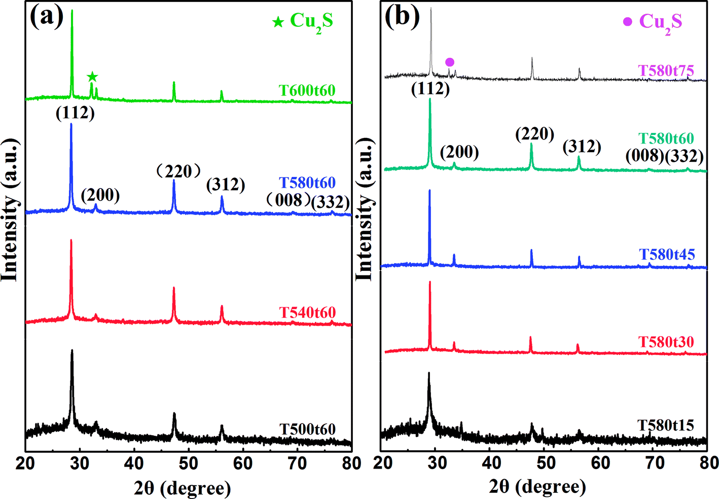 | ||
| Fig. 1 XRD spectra of Cu2InxZn1−xSnS4 (x = 0.4) alloy thin films. (a) Including samples T500t60, T540t60, T580t60 and T600t60 which were annealed under different sulfurization temperature of 500, 540, 580, 600 °C for 60 min, respectively; (b) including samples named T580t15, T580t30, T580t45, T580t60 and T580t75 which were annealed at 580 °C under various sulfurization time of 15, 30, 45, 60, 75 min, respectively. | ||
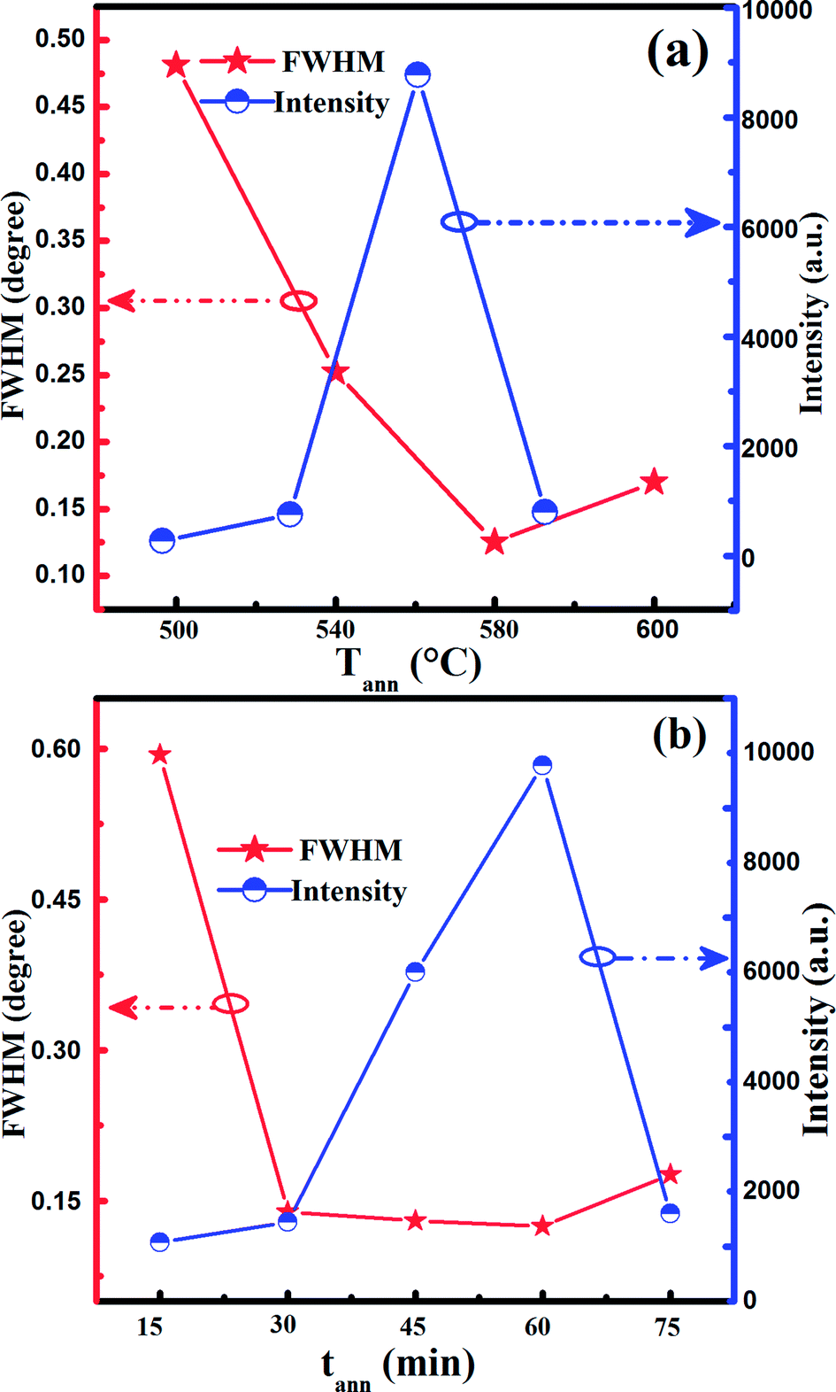 | ||
| Fig. 2 Variation in intensity and the full-width at half-maximum (FWHM) of (112) peaks against various sulfurization temperature and sulfurization time for Cu2InxZn1−xSnS4 (x = 0.4) alloy thin films: (a) including samples T500t60, T540t60, T580t60 and T600t60 which were annealed under different sulfurization temperature of 500, 540, 580, 600 °C for 60 min, respectively; (b) including samples named T580t15, T580t30, T580t45,T580t60 and T580t75 which were annealed at 580 °C under various sulfurization time of 15, 30, 45, 60, 75 min, respectively. | ||
Besides the sulfurization temperature, the sulfurization time is also regarded as one of the susceptive elements for effecting the structure and crystallinity of Cu2InxZn1−xSnS4 (x = 0.4) thin films during annealing process.25 Therefore, we also investigate the influence of the sulfurization time on structure and crystal quality of Cu2InxZn1−xSnS4 (x = 0.4) thin films, and the sulfurization temperature is adopted as 580 °C, which is in the optimized sulfurization temperature. Fig. 1(b) illustrates the XRD patterns of the five Cu2InxZn1−xSnS4 (x = 0.4) samples (named T580t15, T580t30, T580t45, T580t60 and T580t75) which were annealed at 580 °C under various sulfurization time of 15, 30, 45, 60, 75 min, respectively. For the T580t15, T580t30, T580t45 and T580t60 samples, it is found that the four samples have strong diffraction peaks corresponding to (112), (200), (220), (312), (008) and (332) planes of CZTS, particularly, which shows a preferential orientation along the (112) direction implying that the four samples are composed of the CZTS single phase with tetragonal kesterite structure.22 The intensity and FWHM values of (112) peaks of the CZTS thin films annealed at various sulfurization time were calculated and displayed in Fig. 2(b). It is found from Fig. 2(b) that the intensity of (112) peak has been enhanced significantly, manifesting the crystalline quality of Cu2InxZn1−xSnS4 (x = 0.4) thin films are improved as the sulfurization time increases up from 15 to 60 min. It is observed that (112) peak intensity of Cu2InxZn1−xSnS4 (x = 0.4) thin films reaches a maximum value and the corresponding FWHM displays a minimum value of 0.125 under the sulfurization time of 60 min, indicating that the crystalline quality of Cu2InxZn1−xSnS4 (x = 0.4) film has almost reached the best level under the sulfurization time of 60 min. As the sulfurization time increased to 75 min, a weak peak appeared at 31.8°, which is attributed to the (103) peak of the CuS phase (PDF #06-0464).23 This phenomenon is associated with the fact that the CZTS decompose into ternary or binary phases at higher temperature, exactly as the earlier explanation for similar phenomenon of XRD patterns mentioned in Fig. 1(a). According to the results of XRD, we hold perspective that the T580t60 sample is the optimal Cu2InxZn1−xSnS4 thin film which has the best structure properties.
Because the area of single phase is very limited in CZTS system with Zn-rich and Cu-poor conditions, the secondary phases arises easily in CZTS thin films synthesized by different methods.26 It is noticed that three XRD peaks located at 2θ = 29.3°, 48.8° and 57.9° of CZTS overlap with those of copper sulfide and zinc sulfide.27 Thus, the phase purity and crystal quality are often discerned by XRD and Raman measurements. Cu2InxZn1−xSnS4 (x = 0.4) alloy thin films were further characterized by Raman measurement with a 514 nm excitation wavelength to detect the possible secondary phases, as shown in Fig. 3. Panels (a) and (b) of Fig. 3 describe the Raman patterns of the Cu2InxZn1−xSnS4 (x = 0.4) thin films prepared under various sulfurization temperature and sulfurization time. Fig. 3(a) presents the Raman patterns of Cu2InxZn1−xSnS4 (x = 0.4) thin films including T500t60, T540t60, T580t60 and T600t60 samples which were annealed under different sulfurization temperature of 500, 540, 580, 600 °C for 60 min, respectively. It is observed that the T500t60, T540t60 and T580t60 samples exhibit a dominated peak located around at 331 cm−1, which corresponded approximately to the Raman peak of 333 cm−1 assigned to the A1 vibrational mode from the CZTS phase28 and other secondary phases were not detected. This dominated peak arises from the A1 vibration mode of the lattice, where only S-anions are involved.28 It illustrates that the T500t60, T540t60 and T580t60 samples consist of a single phase of kesterite CZTS. As the sulfurization temperature increased up to 600 °C, a weak peak is observed at ∼472 cm−1, which is attributed to the Cu2−xS phase.29 This phenomenon also verifies the decomposition of the CZTS arising from the loss of the tin. This result is consistent with the XRD results. Fig. 3(b) presents the Raman patterns of Cu2InxZn1−xSnS4 (x = 0.4) thin films including T580t15, T580t30, T580t45, T580t60 and T580t75 samples which were annealed at 580 °C under various sulfurization time of 15, 30, 45, 60, 75 min, respectively. In the Raman spectra, an evident major peak at 331 cm−1 can be clearly observed for all samples expect for the T580t75 sample. The peaks can be attributed to CZTS, and other secondary phases were not detected. It illustrates that all samples expect for T580t75 consist of a single phase of kesterite CZTS. For T580t75 sample, one extra peak at 472 cm−1 corresponding to Cu2−xS can be seen. This can be attributed to the longer sulfurization time, which easily allows the formation of secondary phase of Cu2−xS. Raman measurements with a 325 nm excitation wavelength was used to further identify the existence of ZnS, as shown in Fig. 3 insert. The peaks at 343, 695 and 1040 cm−1 could be assigned to R1LO, R2LO and R3LO vibrational modes of ZnS, respectively.30 By analyzing Raman spectra, it can be found that the intensity of the ZnS Raman peaks decreases with increasing sulfurization temperature and sulfurization time, as shown in Fig. 3 insert, indicating a decrease of ZnS content, which are in good agreement with the reported literatures.31 Based on the results of XRD and Raman mentioned above, taking account of crystalline quality of Cu2InxZn1−xSnS4 (x = 0.4) thin films, it is deduced that the optimized sulfurization temperature and sulfurization time should be set to 580 °C and 60 min, respectively.
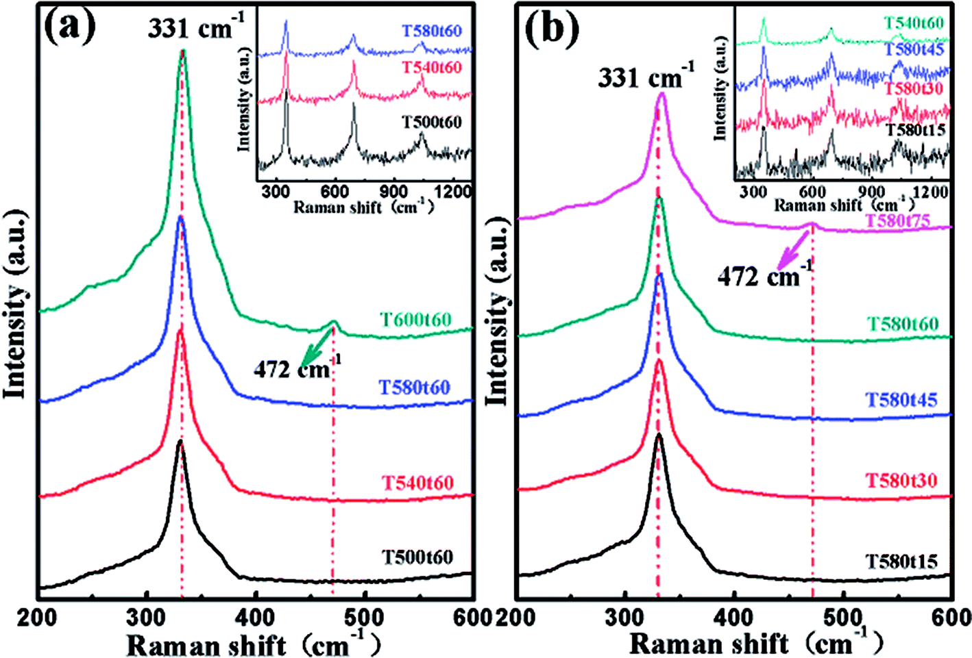 | ||
| Fig. 3 Raman spectra recorded with a 514 nm excitation wavelength of Cu2InxZn1−xSnS4 (x = 0.4) alloy thin films (a) including samples T500t60, T540t60, T580t60 and T600t60 which were annealed under different sulfurization temperature of 500, 540, 580, 600 °C for 60 min, respectively; (b) including samples named T580t15, T580t30, T580t45, T580t60 and T580t75 which were annealed at 580 °C under various sulfurization time of 15, 30, 45, 60, 75 min, respectively. The upper right insets show the main Raman spectra recorded with a 325 nm excitation wavelength of Cu2InxZn1−xSnS4 (x = 0.4) alloy thin films (a) including samples T500t60, T540t60 and T580t60 respectively; (b) including samples named T580t15, T580t30, T580t45 and T580t60, respectively. | ||
So as to ascertain the phase compositions and valence states of the composing elements, the XPS spectra were measured for the T580t60 sample and shown in Fig. 4. Fig. 4(a) is the full-scan XPS spectrum (0–1200 eV), which showed peaks related to C, Cu, Zn, Sn, S and In. The high-resolution scan XPS spectra of the Cu 2p, Zn 2p, Sn 3d, S 2p and In 3d from the T580t60 sample are shown in Fig. 4(b)–(f), respectively. As shown in Fig. 4(b), the narrow scan XPS spectrum of the Cu 2p displays two peaks at 931.2 eV and 951.7 eV, corresponding to Cu 2p3/2 and Cu 2p1/2 with a splitting of 20.5 eV, which is consistent with the standard splitting value of Cu+. So, it can be concluded that Cu exists in the Cu+ state, which is acquired from the reduction of Cu2+ during course of ionic reaction.32 Fig. 4(c) displays the core level XPS spectrum of Zn 2p, which possesses a doublet lied on 1020.8 eV and 1043.9 eV corresponding to the core lines of Zn 2p3/2 and Zn 2p1/2, respectively. This splitting energy value was measured to be 23.1 eV, which also clearly supports that Zn exists in a completely +2 combined-state.33 The Sn 3d5/2 and Sn 3d3/2 peaks are revealed at 485.4 eV and 493.5 eV, as shown in Fig. 3(d). The binding energy of the Sn 3d is nearly consistent with that of Sn4+ in CZTS alloy thin film. It is observed from Fig. 4(e) that the peaks of S 2p are situated at 160.2 eV and 162.8 eV, which is in good agreement with the binding energy of the S in CZTS.34 The binding energies of Zn2+, Cu+, Sn4+ and sulfides are consistent with the reported values in CZTS alloy thin film. Fig. 4(f) depicts the In 3d XPS spectrum of the T580t60 sample. The two strong characteristic peaks at 443.4 eV and 451.0 eV are ascribed to the core levels of In 3d3/2 and In 3d5/2, respectively.35 The binding energy of the In 3d suggests that the chemical value of In is +3. No else XPS peak of the metallic In or other valance state was detected, implying that In has been doped into CZTS successfully.
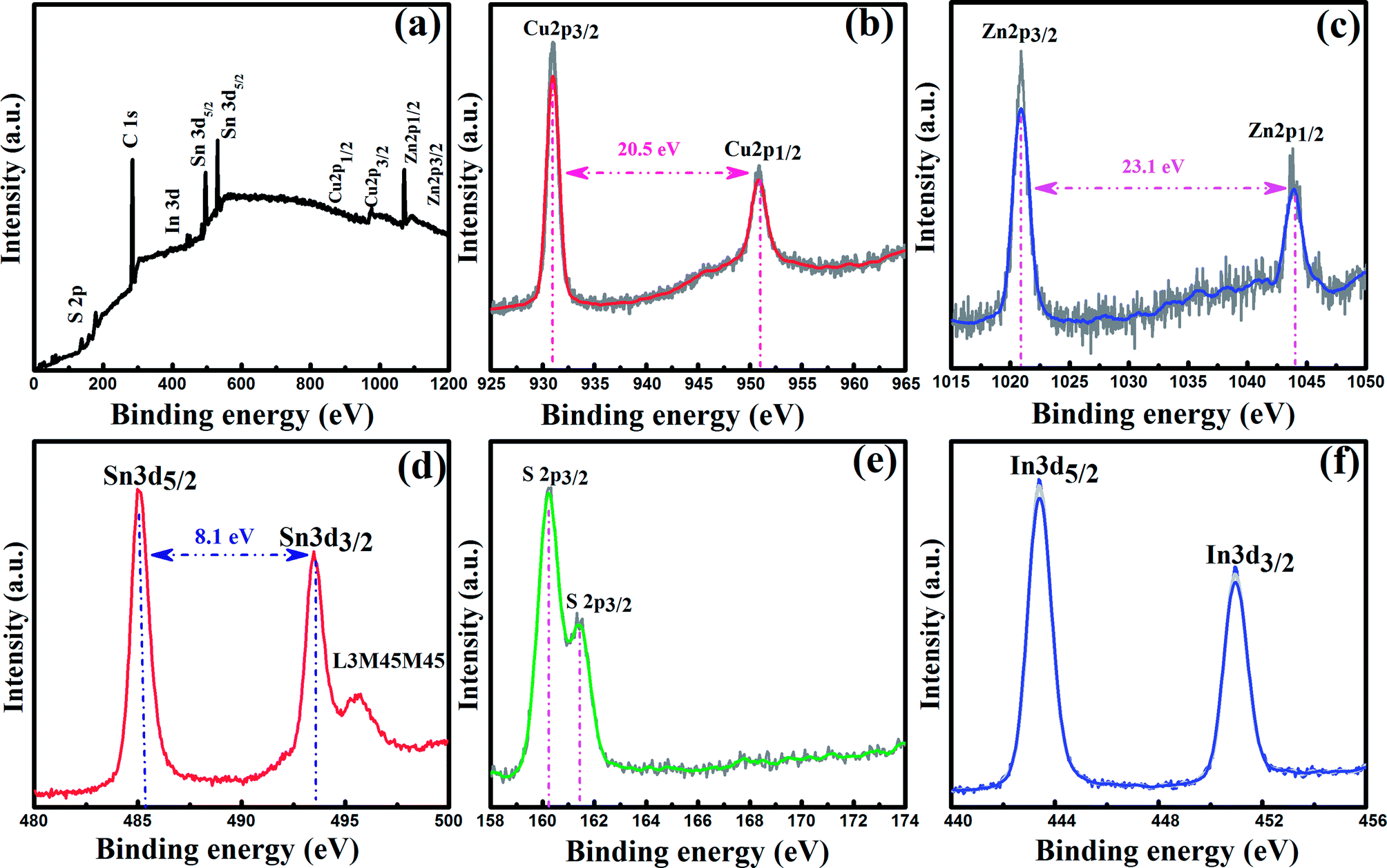 | ||
| Fig. 4 XPS spectra of (a) the full-scan spectrum, (b) Cu 2p, (c) Zn 2p, (d) Sn 3d, (e) S 2p and (f) In 3d for the Cu2InxZn1−xSnS4 (x = 0.4) alloy thin films. | ||
To further determine the detailed microscopic structure of the Cu2InxZn1−xSnS4 (x = 0, x = 0.4) thin films, the TEM measurements were performed. Fig. 5 depicts the TEM images of (a) Cu2InxZn1−xSnS4 (x = 0) thin film (CZTS sample) synthesized under the identical experimental conditions as T580t60 sample, (b) Cu2InxZn1−xSnS4 (x = 0.4) thin film (T580t60 sample), respectively. It can be seen from Fig. 5(a) that the measured interplanar spacing of the crystallographic plane is 0.34 nm, which accords well with the interplanar spacing of the (112) plane of CZTS with tetragonal kesterite structure (JCPDS-26-05757). Additionally, the selected-area electron diffraction (SAED) in Fig. 5(c) shows typical polycrystalline diffraction for the sample, which reveals highly crystalline materials. Fig. 5(b) shows that Cu2InxZn1−xSnS4 (x = 0.4) thin films (T580t60 sample) are arrayed in the (112) direction, and a slightly larger lattice spacing of 0.47 nm in comparison with that (0.34 nm) of CZTS film was measured, which is associated approximately with the spacing of (112) crystal plane of CZTS. It is concluded that some Zn sites in CZTS crystal lattice were substituted by In atoms to form the Cu2InxZn1−xSnS4 thin films, since In has a larger ionic radius (0.80 Å) than Zn (0.74 Å), which is consistent with the results of XPS and XRD analysis. The SAED pattern in Fig. 5(d) suggests that the nanocantilever of the sample is single crystalline tetragonal kesterite because of the well-regulated dot pattern. This phenomenon indicates that the T580t60 sample possesses a relatively preferable structure quality, which is consistent with the earlier opinion proposed from the results of XRD analysis.
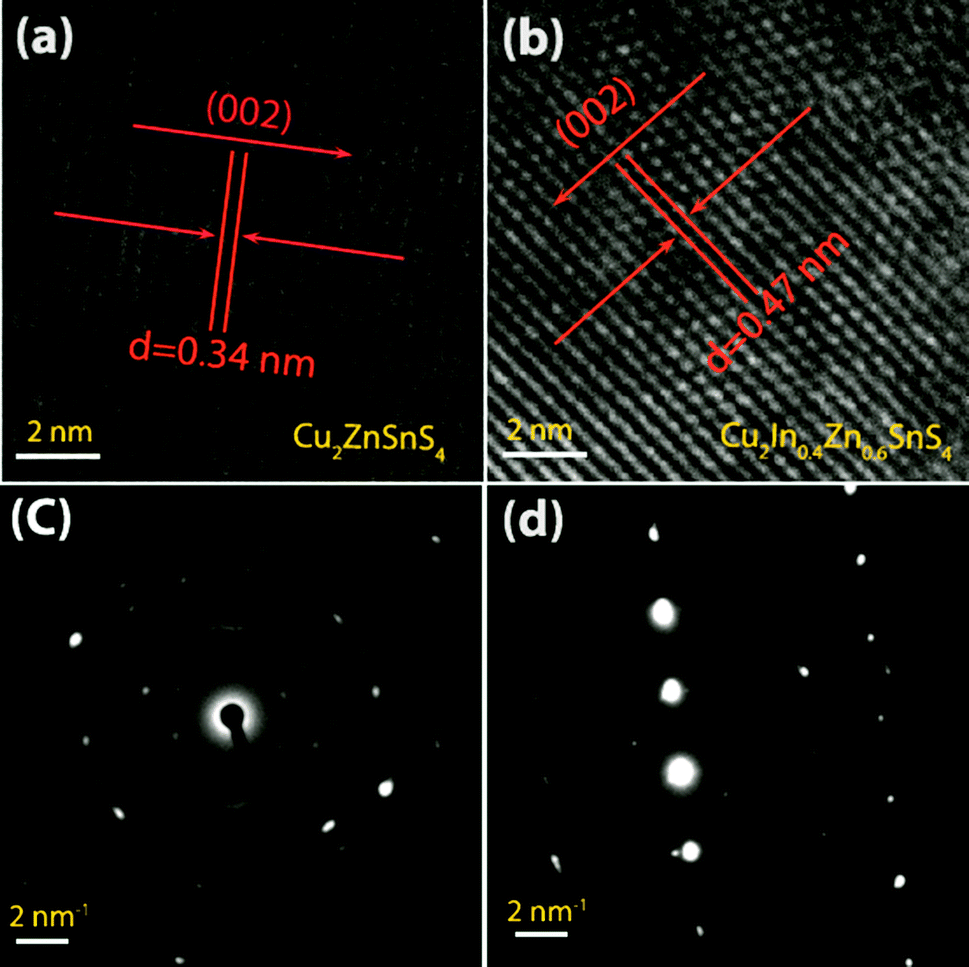 | ||
| Fig. 5 High resolution TEM images of (a) Cu2ZnSnS4 and (b) Cu2InxZn1−xSnS4 (x = 0.4) thin films. SAED pattern of (c) Cu2ZnSnS4 and (d) Cu2InxZn1−xSnS4 (x = 0.4) thin films. | ||
It is well known that the optical and electrical properties of CZTS thin films display a strong rely on the stoichiometry of Cu, Zn, Sn and S in CZTS thin film. Well-controlled atomic contents of Cu, Zn, Sn and S in CZTS thin film has become a key issue for preparing the kesterite CZTS solar cells with high-performance.36 In order to check the composition and concentration of elements for Cu2InxZn1−xSnS4 (x = 0.4) thin films. Energy Dispersive Spectrometry (EDS) was performed for the Cu2InxZn1−xSnS4 (x = 0.4) thin films annealed at different sulfurization temperature and sulfurization time. Table 1 summarizes the composition ratios of the Cu, Zn, Sn, In, S, Cu/(Zn + In + Sn) and Sn/(In + Zn) in the Cu2InxZn1−xSnS4 (x = 0.4) thin films obtained at different sulfurization temperature and sulfurization time. The EDS results verified the existence of Cu, Zn, Sn, In and S elements in the prepared films, as shown in Table 1. The atomic percentages of Sn decreased, while the atomic percentages of S remained relatively constant with the sulfurization temperature and sulfurization time increasing. It manifests that the loss of Sn occurs during the sulfurization process, which is in good agreement with the opinion proposed from the analysis of XRD results. It also was found that the atomic percentages of Zn and Cu increased and the atomic percentages of Sn decreased in the Cu2InxZn1−xSnS4 (x = 0.4) thin films with increasing the sulfurization temperature and sulfurization time, leading to the ratios of Cu/(Zn + In + Sn) and (Zn + In)/Sn in the film increased, as shown in Table 1.
| Temperature (°C) | Time (min) | Cu (at%) | Zn (at%) | Sn (at%) | In (at%) | S (at%) | Cu/(Zn + In + S) | (Zn + In)/Sn |
|---|---|---|---|---|---|---|---|---|
| 500 | 60 | 24.6 | 13.8 | 10.23 | 4.37 | 47 | 0.86 | 1.70 |
| 540 | 60 | 25.04 | 13.83 | 10.13 | 4.30 | 46.7 | 0.88 | 1.78 |
| 580 | 60 | 25.05 | 14.1 | 10.02 | 4.22 | 47.61 | 0.90 | 1.82 |
| 600 | 60 | 25.59 | 14.2 | 9.52 | 4.25 | 46.44 | 0.91 | 1.93 |
| 580 | 15 | 25.05 | 13.5 | 10.59 | 4.09 | 46.77 | 0.87 | 1.66 |
| 580 | 30 | 25.08 | 14.03 | 10.38 | 4.14 | 46.37 | 0.87 | 1.75 |
| 580 | 45 | 25.62 | 14.28 | 10.29 | 4.14 | 45.67 | 0.89 | 1.79 |
| 580 | 60 | 25.69 | 14.85 | 9.95 | 4.03 | 45.48 | 0.89 | 1.89 |
| 580 | 75 | 26.76 | 14.89 | 9.82 | 4.24 | 44.29 | 0.92 | 1.94 |
Well-adopted sulfurization temperature and sulfurization time are crucial to acquire the large grain and a small amount voids in CZTS thin film. Fig. 6 shows the SEM surface images of Cu2InxZn1−xSnS4 thin films annealed at different sulfurization temperature ((a) 500 °C, (b) 540 °C, (c) 580 °C and (d) 600 °C) for 60 min and annealed at 580 °C with different sulfurization time ((e) 15 min, (f) 30 min, (g) 45 min, (h) 60 min and (i) 75 min). The remarkable influence of the sulfurization temperature and sulfurization time on the microstructure of Cu2InxZn1−xSnS4 thin films is clearly observed. With the sulfurization temperature increasing from 500 to 580 °C, the grain size of Cu2InxZn1−xSnS4 thin films increased and the surface of the thin films became smooth and dense, as shown in Fig. 6(a–c). At higher temperature, the ions have a greater reactivity, which facilitates the growth of the nanocrystals. However, the grain size decreased with sequentially increasing sulfurization temperature up to 600 °C, as shown in Fig. 6(d), which may be ascribed to the loss of Sn element during the sulfurization process. Formation of voids on the surface is evident for the T500t60, T540t60 and T600t60 samples. It is clear that the relatively compact surface with densely packed grains is observed for sample T580t60, as shown in Fig. 6(c). The SEM measurements of the Cu2InxZn1−xSnS4 thin films obtained at different sulfurization time of 15, 30, 45, 60 and 75 min are shown in Fig. 6(e–i). It showed that the Cu2InxZn1−xSnS4 thin film obtained at the sulfurization time of 15 min is composed of nanometer grains, and the grains also stack loosely. Moreover, there are some holes in the Cu2InxZn1−xSnS4 thin film surface, as shown in Fig. 6(e). When increasing the sulfurization time to 30 min, the grain of Cu2InxZn1−xSnS4 thin film increases and gets compact, as shown in Fig. 6(f). However, the surface of Cu2InxZn1−xSnS4 thin film shows some smaller grains, which are not favorable to the formation of the CZTS solar cells with high efficiency. As the sulfurization time increased to 60 min, the grains grew sharply to micrometer scale and stack densely, as shown in Fig. 6(h). For solar cell application, it is known that the CZTS absorber thin film with large grain size, smooth surface and less grain boundaries are desirable to the preparation of high PCE solar cell, because the larger grains will promote the transport of photo-generated carriers, which could lead to minimize grain boundary recombination.37 So, the T580t60 sample is well suited for application as the absorption layer in photovoltaic devices. Further increasing the sulfurization time to 75 min, the grain size decreases and the grains stack loosely, as shown in Fig. 6(i). The noticeable change for Cu2InxZn1−xSnS4 (x = 0.4) morphology corresponds well to the XRD results discussed above. The decrease of the grain size may be because of the loss of Sn during the sulfurization process, and there were some secondary phases (like CuS) for T580t75 sample.
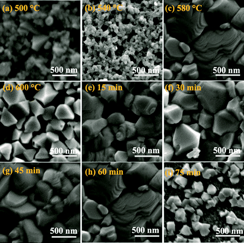 | ||
| Fig. 6 SEM images of the Cu2InxZn1−xSnS4 (x = 0.4) alloy thin films annealed at 500 °C (a), 540 °C (b), 580 °C (c), 600 °C (d), 15 min (e), 30 min (f), 45 min (g), 60 min (h), and 75 min (i). | ||
Table 2 depicts the electrical properties of as-grown CZTS, as-grown Cu2InxZn1−xSnS4 (x = 0.4) and Cu2InxZn1−xSnS4 (x = 0.4) thin films which were annealed at various sulfurization temperature and sulfurization time, respectively. In order to better compare and clarify the influence of annealing condition and In doping on electrical properties of Cu2InxZn1−xSnS4 (x = 0.4) thin films, pure CZTS thin films were deposited on SLG substrates under the same experimental conditions as Cu2InxZn1−xSnS4 (x = 0.4) thin film, which were showed in Table 2, too. As summarized in Table 2, the as-grown CZTS thin film exhibits a bad p-type conductivity due to its numerous intrinsic defects. With the incorporation of In, the as-grown Cu2InxZn1−xSnS4 (x = 0.4) thin film remained p-type behavior with a carrier concentration of 9.46 × 1013 cm−3, a mobility of 0.91 cm2 V−1 s−1 and a resistivity of 8.99 × 10² Ω cm, which are considerably weaker than that of pure CZTS. According to the results of XRD, XPS and TEM mentioned above, In has been doped into the CZTS and the trivalent In substituted for the divalent Zn site to form the InZn donor, then introducing some electrons into the system. For this reason, the hole concentration of CuZn would be decreased by the electrons that InZn donor provided, consequently leading to the worse p-type conduction property.
| Sample | Temperature (°C) | Time (min) | ρ (Ω cm) | n (cm−3) | μ (cm−2 V−1 s−1) | Conduction type |
|---|---|---|---|---|---|---|
| CZTS | 300 | 5 | 9.29 × 101 | 2.09 × 10¹⁴ | 0.21 | p |
| Cu2InxZn1−xSnS4 | 300 | 5 | 8.99 × 101 | 9.46 × 10¹³ | 0.91 | p |
| T500t60 | 500 | 60 | 1.38 × 101 | 5.47 × 10¹⁷ | 0.76 | p |
| T540t60 | 540 | 60 | 3.73 × 101 | 2.47 × 10¹⁷ | 0.77 | p |
| T580t60 | 580 | 60 | 6.81 × 10² | 9.06 × 10¹⁶ | 3.35 | p |
| T580t15 | 580 | 15 | 3.92 × 101 | 1.32 × 10¹⁷ | 1.22 | p |
| T580t30 | 580 | 30 | 2.61 × 101 | 1.08 × 10¹⁷ | 2.24 | p |
| T580t45 | 580 | 45 | 9.59 × 101 | 0.98 × 10¹⁷ | 2.25 | p |
| T580t60 | 580 | 60 | 6.81 × 10² | 9.06 × 10¹⁶ | 3.35 | p |
Table 2 also displays the electrical properties of the Cu2InxZn1−xSnS4 (x = 0.4) thin films annealed at different sulfurization temperature. It was found that all Cu2InxZn1−xSnS4 (x = 0.4) thin films showed the p-type (hole mediated) conductivity behavior. It has been reported that Cu substituting Zn site (Cuzn) are the main of acceptor in stoichiometric CZTS due to their low formation energies and shallow level, which is responsible for the p-type conduction of CZTS.38 It was observed that the carrier concentration decreased from 5.47 × 10¹⁷ to 9.06 × 1016 cm−3 as the sulfurization temperature increased from 500 to 580 °C. However, the change tendency of the resistivity and the mobility is contrary with that of the carrier concentration. This may be due to that with the sulfurization temperature increasing, the crystalline quality is improved and the grain boundaries become less, leading to the reduction of the carrier concentration and increment of the mobility.39
Xiao et al. have pointed out that the conduction characteristics of the CZTS thin films are also affected greatly by sulfurization time.25 Hence, the effect of sulfurization time on the electrical properties of Cu2InxZn1−xSnS4 (x = 0.4) thin films was investigated under the fixed sulfurization temperature of 580 °C, as displayed in Table 2. It is observed that all the Cu2InxZn1−xSnS4 thin films synthesized at different sulfurization time behave p-type conductivity. Also, it was found that the carrier concentration of the film decreased obviously from 1.32 × 10¹⁷ to 9.06 × 1016 cm−3 with the sulfurization time increasing from 15 to 60 min, attributed to the increase of the atomic ratio of Cu/(Zn + Sn) in the film, which has been proved in the foregoing EDS result. The increase of the atomic ratio of Cu/(Zn + Sn) could produce the decrease of the CuZn antisite acceptor defect and the increase of CuZn + SnZn deep donor defect, leading to the reduction of the carrier concentration.36 The Hall mobility of the Cu2InxZn1−xSnS4 thin films were increased from 1.22 to 3.35 cm2 V−1 s−1, which is possibly ascribed to the fact that the crystalline quality is enhanced and the grain boundaries become less as the sulfurization time increases.
For the sake of studying the effect of the sulfurization temperature and sulfurization time on the band gap (Eg) of Cu2InxZn1−xSnS4 (x = 0.4) thin films, the absorption characteristic of the Cu2InxZn1−xSnS4 (x = 0.4) prepared at different sulfurization temperature and sulfurization time were researched by an UV-Vis-NIR spectrophotometer. According the optical absorption spectra, the band gap value of the Cu2InxZn1−xSnS4 (x = 0.4) is obtained by using the relation:40
| (αhν)1/n = B[(hν − Eg)1/2/hν] | (1) |
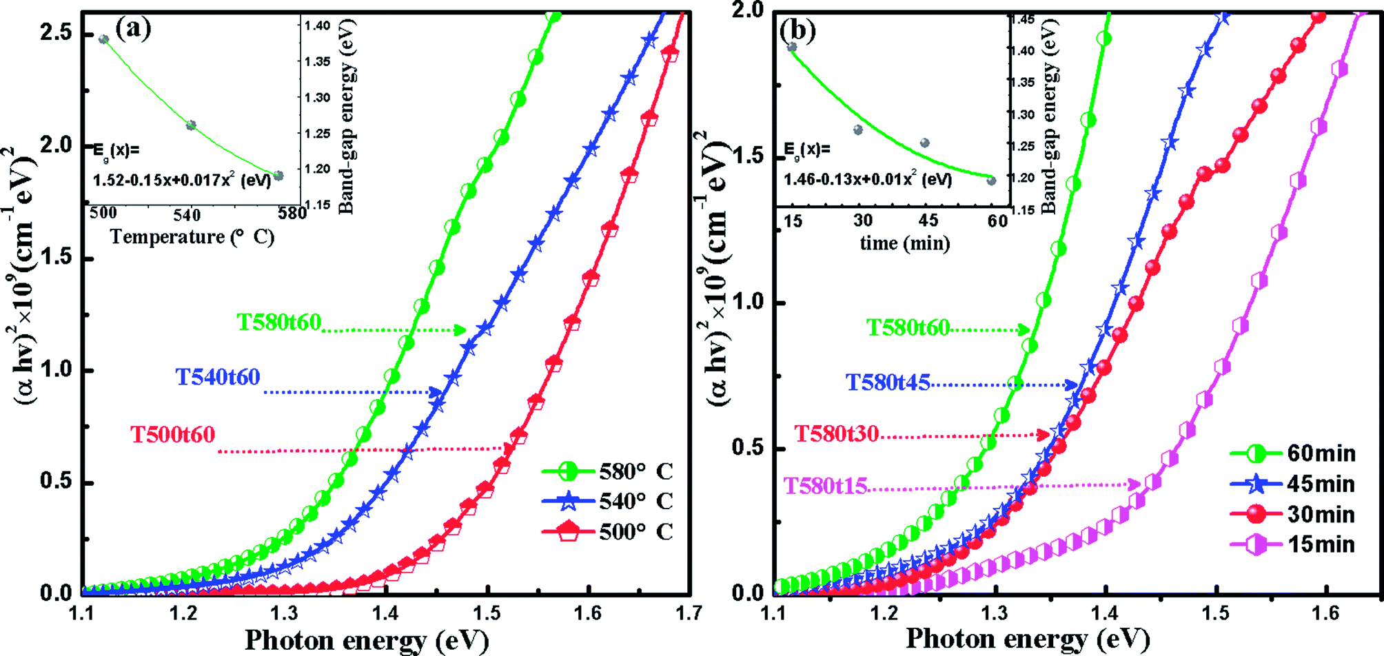 | ||
| Fig. 7 Plot of (αhν)2 against hν for Cu2InxZn1−xSnS4 (x = 0.4) alloy thin films: (a) including samples T500t60, T540t60 and T580t60 which were annealed under different sulfurization temperature of 500, 540 and 580 for 60 min, respectively; (b) including samples named T580t15, T580t30, T580t45 and T580t60 which were annealed at 580 °C under various sulfurization time of 15, 30, 45, 60 min, respectively. The upper left insets show the variation of band gaps of Cu2InxZn1−xSnS4 (x = 0.4) alloy thin films. | ||
Fig. 8 shows the current–voltage (J–V) characteristics of Cu2InxZn1−xSnS4 (x = 0) device (CZTS) (red solid circulars) and Cu2InxZn1−xSnS4 (x = 0.4) (blue solid starts) device which were synthesized under the identical experimental conditions, respectively. All device parameters like Jsc, Voc and fill-factor corresponding to the Cu2InxZn1−xSnS4 (x = 0.4) absorber are much higher compared to the pure CZTS absorber and yields a power conversion efficiency of 2.89% under 1 sun condition, as shown in Table 3. From J–V curves, the series resistance (RS) is calculated to be ∼42 Ω cm2 and shunt resistance (RSH) is ∼137 Ω cm2 in the Cu2InxZn1−xSnS4 (x = 0.4) device whereas for CZTS device RS ∼ 65 Ω cm2 and RSH ∼ 88 Ω cm2 for the CZTS device. The decrease in series resistances and increase of shunt resistance could be a result of increased grain size and reduction of defect density in the Cu2InxZn1−xSnS4 (x = 0.4) device. These improvements in series and shunt resistance results in the improved current density and fill factor. We also observed a significant improvement in Voc of about 90 mV. This is mainly due to the reduction of CuZn antisite defects which could reduce band-tailing and yield high band bending at the interface of the absorber and buffer layer. This yielded an enhancement in Voc, Jsc and fill factor of the device. Thus, In substitution improves the overall performance of CZTS solar cell and should be pursued as a solution to the Voc deficit issue in the Cu-kesterite thin film solar cells.
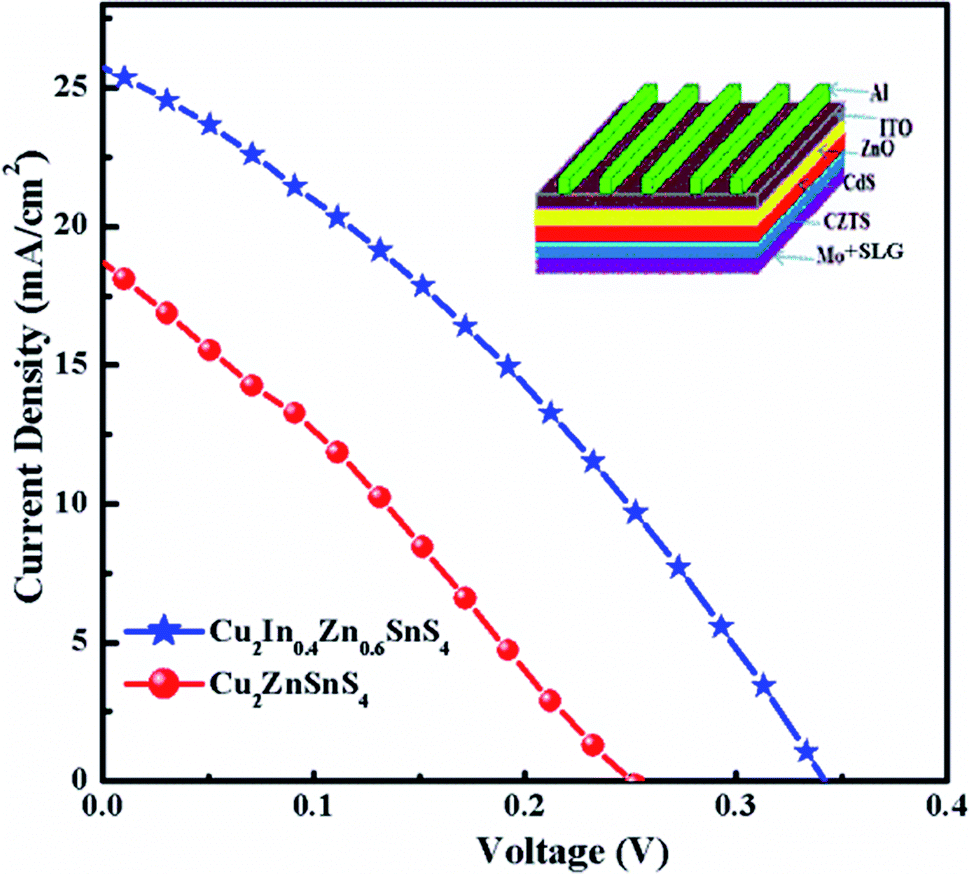 | ||
| Fig. 8 Current–voltage characteristics of the CZTS and Cu2InxZn1−xSnS4 (x = 0.4) devices, the device schematic structure has been shown in inset. | ||
| Device | Active area | Voc (V) | Jsc (mA cm−2) | FF | PCE |
|---|---|---|---|---|---|
| CZTS | 0.19 cm2 | 0.25 | 18.69 | 30.59 | 1.44 |
| Cu2InxZn1−xSnS4 (x = 0.4) | 0.19 cm2 | 0.34 | 25.73 | 32.62 | 2.89 |
4. Conclusion
In conclusion, the Cu2InxZn1−xSnS4 (x = 0.4) alloy thin films have been successfully synthesized on SLG substrates at different sulfurization temperature and sulfurization time by a simple low-cost sol–gel method followed by rapid annealing technique. The structure, optical and electrical properties of Cu2InxZn1−xSnS4 (x = 0.4) alloy thin films are greatly dependent on sulfurization temperature and sulfurization time. XRD results indicated the Cu2InxZn1−xSnS4 (x = 0.4) alloy thin film has the best crystalline quality at the optimized sulfurization condition of 580 °C for 60 min, respectively. Hall measurements results showed that all Cu2InxZn1−xSnS4 alloy thin films showed p-type conduction characteristics, the hole concentration decreased and the mobility increased with the increase of sulfurization temperature and sulfurization time, ascribing to the improvement of the crystalline quality and the reduction of the grain boundaries. The optimal p-type Cu2InxZn1−xSnS4 (x = 0.4) film with a mobility of 3.35 cm2 V−1 s−1 and carrier concentration of 9.06 × 1016 cm−3 also was obtained at the optimized sulfurization condition of 580 °C for 60 min, respectively. The Eg of all the Cu2InxZn1−xSnS4 alloy thin films is smaller than that of the undoped CZTS on account of the In doping. The Eg of Cu2InxZn1−xSnS4 (x = 0.4) alloy thin films is decreased from 1.38 to 1.19 eV with the increase of the sulfurization temperature and sulfurization time, which is attributed to the decrease of the residual organic precursor compounds and the increase of Cu/(Zn + Sn) atomic ratio in the films. The Cu2InxZn1−xSnS4 (x = 0.4) solar cell obtained at an optimized sulfurization condition of 580 °C for 60 min demonstrates a power conversion efficiency of 2.89%.Conflicts of interest
There are no conflicts to declare.Acknowledgements
The authors would like to thank financial support of the National Natural Science Foundation of China under Grant No. 61505067, 11254001, 61475063, 61605059, 21576111, 61378085. The National Key Research and Development Program of China under Grant No. 2017YFF0108607, the Program for the development of Science and Technology of Jilin province Grant No. 20150520086JH.References
- D. B. Mitzi, O. Gunawan, T. K. Todorov, K. Wang and S. Guha, Sol. Energy Mater. Sol. Cells, 2011, 95, 1421–1436 CrossRef CAS.
- A. Walsh, S. Chen, S. Wei and X. Gong, Adv. Energy Mater., 2012, 2, 400–409 CrossRef CAS.
- H. Sugimoto, C. Liao, H. Hiroi, N. Sakai and T. Kato, IEEE 39th Photovoltaic Specialists Conference (PVSC), 2013, pp. 3208–3211 Search PubMed.
- W. Wang, M. T. Winkler, O. Gunawan, T. Gokmen, T. K. Todorov, Y. Zhu and D. B. Mitzi, Adv. Energy Mater., 2014, 4, 1301465 CrossRef.
- P. Jackson, D. Hariskos, R. Wuerz, O. Kiowski, A. Bauer, T. M. Friedlmeier and M. Powalla, Phys. Status Solidi A, 2015, 9, 28–31 CAS.
- D. B. Mitzi, O. Gunawan, T. K. Todorov and D. A. R. Barkhouse, Philos. Trans. R. Soc., 2013, 371, 1–22 Search PubMed.
- S. Tajima, T. Itoh, H. Hazama, K. Ohishi and R. Asahi, Appl. Phys. Express, 2015, 8, 082302 CrossRef.
- H. S. Duan, W. Yang, B. Bob, C. J. Hsu, B. Lei and Y. Yang, Adv. Funct. Mater., 2013, 23, 1466–1471 CrossRef CAS.
- C. J. Hages, S. Levcenco, C. K. Miskin, J. H. Alsmeier, D. Ras and R. G. Wilks, Prog. Photovoltaics, 2015, 23, 376–384 CAS.
- T. Todorov, K. Reuter and D. Mitzi, Adv. Mater., 2010, 22, 156–159 CrossRef PubMed.
- Z. Su, J. M. R. Tan, X. Li, X. Zeng, S. K. Batabyal and L. H. Wong, Adv. Energy Mater., 2015, 5, 1500682 CrossRef.
- C. Hages, S. Levcenco, C. Miskin, J. Alsmeier, D. Abou-Ras, R. Wilks, M. Bär, T. Unold and R. Agrawal, Prog. Photovoltaics, 2015, 23, 376–384 CAS.
- D. H. Kuo and M. Tsega, Jpn. J. Appl. Phys., 2014, 53, 035801 CrossRef.
- J. Kim, H. Hiroi, T. K. Todorov, O. Gunawan, M. Kuwahara, T. Gokmen, D. Nair, M. Hopstaken, S. Y. Lee and H. Sugimoto, Adv. Mater., 2014, 26, 7427–7431 CrossRef CAS PubMed.
- Y. R. Ying, Y. J. Wu, Y. Zhang, Z. W. Wang, M. B. Wei and B. Yao, Superlattices Microstruct., 2017, 111, 579–590 CrossRef.
- G. Chen, J. Li, M. Wu, J. Liu, F. Lai and C. Zhu, Mater. Lett., 2015, 159, 32–34 CrossRef CAS.
- K. V. Gurav, S. W. Shin, U. M. Patil, M. P. Suryawanshi, S. M. Pawar, M. G. Gang, S. A. Vanalakar, J. H. Yun and J. H. Kim, J. Alloys Compd., 2015, 631, 178–182 CrossRef CAS.
- D. C. Nguyen, S. Ito and D. V. A. Dung, J. Alloys Compd., 2015, 632, 676–680 CrossRef CAS.
- S. Ranjbar, M. R. Rajesh Menon, P. A. Fernandes and A. F. Cunha, Thin Solid Films, 2015, 582, 188–192 CrossRef CAS.
- S. Hwang, D. H. Kim, D. H. Son, K. J. Yang, D. Nam, H. Cheong and J. K. Kang, Sol. Energy Mater. Sol. Cells, 2015, 143, 218–225 CrossRef CAS.
- M. G. Gang, K. V. Gurav, S. W. Shin, C. W. Hong, J. H. Min, M. P. Suryawanshi, S. A. Vanalakar, D. S. Lee and J. H. Kim, Phys. Status Solidi C, 2015, 12, 713–716 CrossRef CAS.
- Y. B. Kishor Kumar, G. Suresh Babu, P. Uday Bhaskar and V. Sundar Raja, Sol. Energy Mater. Sol. Cells, 2009, 93, 1230–1237 CrossRef.
- S. Thiruvenkadam, D. Jovina and A. Leo Rajesh, Sol. Energy, 2014, 106, 166–170 CrossRef CAS.
- T. Shiyani, M. Patel and I. Mukhopadhyay, IETE Technical Review, 2016, 33, 2–6 CrossRef.
- Z. Y. Xiao, B. Yao, Y. F. Li, Z. H. Ding, Z. M. Gao, H. F. Zhao and G. Wang, ACS Appl. Mater. Interfaces, 2016, 8, 17334–17342 CAS.
- D. M. Berg, M. Arasimowicz, R. Djemour, L. Gütay, S. Siebentritt, S. Schorr, X. Fontané, V. Izquierdo-Roca, A. Pérez-Rodriguez and P. J. Dale, Thin Solid Films, 2014, 569, 113–123 CrossRef CAS.
- A. Khare, B. Himmetoglu, M. Johnson, D. J. Norris, M. Cococcioni and E. S. Aydil, J. Appl. Phys., 2012, 118, 083707 CrossRef.
- D. Dumcenco and Y. S. Huang, Opt. Mater., 2013, 35, 419–425 CrossRef CAS.
- S. Thiruvenkadam, D. Jovina and A. Leo Rajesh, Sol. Energy, 2014, 106, 166–170 CrossRef CAS.
- J. J. Scragg, T. Ericson, X. Fontane, V. Izquierdo-Roca, A. Perez-Rodríguez, T. Kubart, M. Edoff and C. Platzer-Bjorkma, Prog. Photovoltaics, 2014, 22, 10–17 CAS.
- O. Vigil-Galan, M. Espíndola-Rodríguez, M. Courel, X. Fontane, D. Sylla, V. Izquierdo-Roca, A. Fairbrother, E. Saucedo and A. Perez-Rodríguez, Sol. Energy Mater. Sol. Cells, 2013, 17, 246e250 Search PubMed.
- H. Y. Chen, S. M. Yu, D. W. Shin and J. B. Yoo, Nanoscale Res. Lett., 2010, 5, 217–223 CrossRef CAS PubMed.
- M. Danilson, M. Altosaar, M. Kauk, A. Katerski, J. Krustok and J. Raudoja, Thin Solid Films, 2011, 519, 7407–7411 CrossRef CAS.
- M. Tsega, F. B. Dejene and D. H. Kuo, J. Alloys Compd., 2015, 642, 140–147 CrossRef CAS.
- F. Jiang, T. Harada, Y. Kuang, T. Minegishi, K. Domen and S. Ikeda, J. Am. Chem. Soc., 2015, 137, 13691–13697 CrossRef CAS PubMed.
- M. Y. Yeh, P. H. Lei, S. H. Lin and C. D. Yang, Materials, 2016, 9, 526 CrossRef PubMed.
- J. Li and D. B. Mitzi, ACS Nano, 2011, 5, 8613–8619 CrossRef CAS PubMed.
- A. Walsh, S. Chen, S. H. Wei and X. G. Gong, Adv. Energy Mater., 2012, 2400–2409 Search PubMed.
- B. Long, S. Y. Cheng, Y. F. Lai, Y. F. Zhou, J. L. Yu and Q. Zheng, Thin Solid Films, 2014, 573, 117–121 CrossRef CAS.
- Y. F. Li, B. Yao, Y. M. Lu, Z. P. Wei, Y. Q. Gai, C. J. Zheng, B. H. Li, D. Z. Shen, X. W. Fan and Z. K. Tang, Appl. Phys. Lett., 2007, 91, 2115 Search PubMed.
- K. Tanaka, Y. Fukui, N. Moritake and H. Uchiki, Sol. Energy Mater. Sol. Cells, 2011, 95, 838–842 CrossRef CAS.
Footnote |
| † Electronic supplementary information (ESI) available. See DOI: 10.1039/c7ra12289f |
| This journal is © The Royal Society of Chemistry 2018 |