
 Open Access Article
 This Open Access Article is licensed under a Creative Commons Attribution-Non Commercial 3.0 Unported Licence
Tunable graphene doping by modulating the nanopore geometry on a SiO2/Si substrate†
Namsoo Lim‡
a,
Tae Jin Yoo‡a,
Jin Tae Kim b,
Yusin Pakc,
Yogeenth Kumaresana,
Hyeonghun Kima,
Woochul Kima,
Byoung Hun Lee*a and
Gun Young Jung*a
b,
Yusin Pakc,
Yogeenth Kumaresana,
Hyeonghun Kima,
Woochul Kima,
Byoung Hun Lee*a and
Gun Young Jung*a
aSchool of Materials Science and Engineering, Gwangju Institute of Science and Technology (GIST), Gwangju, 500-712, Republic of Korea. E-mail: gyjung@gist.ac.kr; bhl@gist.ac.kr
bCreative Future Research Laboratory, Electronics and Telecommunications Research Institute, 218, Gajeong-ro Yuseong, Daejeon 305-700, Republic of Korea
cPhysical Science and Engineering Division, King Abdullah University of Science and Technology (KAUST), Thuwal 23955-6900, Saudi Arabia
First published on 28th February 2018
Abstract
A tunable graphene doping method utilizing a SiO2/Si substrate with nanopores (NP) was introduced. Laser interference lithography (LIL) using a He–Cd laser (λ = 325 nm) was used to prepare pore size- and pitch-controllable NP SiO2/Si substrates. Then, bottom-contact graphene field effect transistors (G-FETs) were fabricated on the NP SiO2/Si substrate to measure the transfer curves. The graphene transferred onto the NP SiO2/Si substrate showed relatively n-doped behavior compared to the graphene transferred onto a flat SiO2/Si substrate, as evidenced by the blue-shift of the 2D peak position (∼2700 cm−1) in the Raman spectra due to contact doping. As the porosity increased within the substrate, the Dirac voltage shifted to a more positive or negative value, depending on the initial doping type (p- or n-type, respectively) of the contact doping. The Dirac voltage shifts with porosity were ascribed mainly to the compensation for the reduced capacitance owing to the SiO2–air hetero-structured dielectric layer within the periodically aligned nanopores capped by the suspended graphene (electrostatic doping). The hysteresis (Dirac voltage difference during the forward and backward scans) was reduced when utilizing an NP SiO2/Si substrate with smaller pores and/or a low porosity because fewer H2O or O2 molecules could be trapped inside the smaller pores.
Introduction
Since the paper by Andre Geim and Konstantin Novoselov1 that demonstrated the first graphene device, graphene-related research has expanded rapidly. The expected properties of graphene have been demonstrated in a relatively short time,2–5 and related studies are still ongoing. Graphene has an ultra-high mobility of 200![[thin space (1/6-em)]](https://www.rsc.org/images/entities/char_2009.gif) 000 cm2 V−1 s−12 and an excellent thermal conductivity of 5000 W mK−1,3 making graphene a promising candidate for next-generation electronic material. Moreover, graphene absorbs a broad range of electromagnetic waves from the UV to far-IR regions5–8 and exhibits a fast carrier saturation velocity followed by a short carrier life-time,9,10 which are very promising properties for ultra-fast optoelectronic devices. Furthermore, despite its high optical transmittance (97.7%), graphene shows a high electrical conductivity11,12 as well as high flexibility and stretchability.4 These properties make graphene a promising candidate material for use in a transparent electrode.13,14 The development of an effective doping technique for graphene is necessary to exploit these excellent properties of graphene in a wide range of (opto-)electronic devices. Graphene doping is crucial for realizing the p/n-junction, which is the basic unit for electronic circuits,15 and for the effective control of graphene's Fermi level for compatibility with other circuit elements.16
000 cm2 V−1 s−12 and an excellent thermal conductivity of 5000 W mK−1,3 making graphene a promising candidate for next-generation electronic material. Moreover, graphene absorbs a broad range of electromagnetic waves from the UV to far-IR regions5–8 and exhibits a fast carrier saturation velocity followed by a short carrier life-time,9,10 which are very promising properties for ultra-fast optoelectronic devices. Furthermore, despite its high optical transmittance (97.7%), graphene shows a high electrical conductivity11,12 as well as high flexibility and stretchability.4 These properties make graphene a promising candidate material for use in a transparent electrode.13,14 The development of an effective doping technique for graphene is necessary to exploit these excellent properties of graphene in a wide range of (opto-)electronic devices. Graphene doping is crucial for realizing the p/n-junction, which is the basic unit for electronic circuits,15 and for the effective control of graphene's Fermi level for compatibility with other circuit elements.16
Graphene doping techniques have been explored with the following representative doping methods.17–19 The first type is electrostatic doping, which is the most common doping effect that occurs in the graphene field effect transistor (G-FET) structure. The main advantage of this approach is that the doping level is tunable by the gate potential without any implantation of additional dopants. The second type is contact doping. As graphene is a one-atom-thick two-dimensional (2D) material (t ∼ 0.34 nm) that is very sensitive to its surroundings, it is easily doped by merely contacting a material; for example, graphene can be doped at 1011 charges per cm2 by contacting a SiO2 surface.20,21 The contact doping effect can be much enhanced in the case of a metal contact, as shown by theoretical22,23 and experimental24 results. Usually, the contact doping is an unavoidable phenomenon that is provided by the underlying substrate or during the electrode deposition. The third type is chemical doping. This effect is generated by the adsorbed molecules on the graphene surface in vapor or liquid states. Generally, compounds such as nitric acid,25 metal chlorides, organic molecules,26 and water1,27 are used as p-type dopants, and compounds such as ammonia1,28 and NO2 (ref. 29–31) are used as n-type dopants. Finally, the fourth type is substitution doping. Here, some of the carbon atoms in the graphene lattice are replaced by other atoms (mainly boron (B) or nitrogen (N)), similar to the silicon-doping techniques.17,32,33 Using this technique, the bandgap of graphene can be opened;32 however, substitution doping leads to inevitable lattice breakages, resulting in low-quality graphene sheets.17
In this paper, we used SiO2/Si substrates having nanopores with different porosities and pitches (NP SiO2/Si substrate) to tune the doping state of the transferred graphene in contact with these substrates. Laser interference lithography (LIL) was used to prepare the pitch- and diameter-tunable nanopores. The doping state of the transferred graphene was characterized by Raman spectroscopy. Bottom-contact G-FETs were fabricated on the NP SiO2/Si substrates to observe the Dirac voltage shift due to the porosity-induced contact doping together with the SiO2–air heterostructured dielectric layer-induced electrostatic doping within the aligned nanopores. The effects of porosity and pitch on the Dirac voltage shift were also investigated. It was found that the direction of the Dirac voltage shift was determined by the initial doping polarity of graphene in contact with the underlying substrate.
Experimental
Preparation of the NP SiO2/Si substrates (Scheme 1)
Laser interference lithography (LIL) was used to prepare the NP SiO2/Si substrates having different porosities at different pitches. A 300 nm-thick SiO2/Si wafer (highly p-doped Si, QL Electronics Co., China) was cleaned sequentially in acetone, iso-propyl alcohol (IPA), and deionized water with sonication for 10 min. A 10 nm-thick Cr layer was deposited on the substrate by an electron beam evaporator. Then, a bottom antireflection coating (BARC) layer (100 nm thick, AZ BARLi II 90, MicroChemicals, GmbH, Germany) and a negative photoresist (350 nm thick, AZ nLOF 2020, MicroChemicals GmbH, Germany) were spin-coated in sequence at 4000 rpm for 40 s each. Each spin-coating step was followed by 1 min post-baking at 110 °C. The sample was double-exposed with a He–Cd laser (λ = 325 nm) and developed in a developing solution (AZ 300 MIF, MicroChemicals GmbH, Germany) to produce an array of nanopores. The exposed BARC and Cr layers within the developed nanopores were selectively etched away by O2 plasma etching and with a Cr-wet etchant (CR-7, Cyantek corporation, USA) in sequence. Afterward, the photoresist and BARC layers were eliminated by immersing in a polymer remover (EKC 830, DuPont, USA), leaving the Cr nanopore array, which was used as a mask for etching of the underlying SiO2 with CF4 plasma. By eliminating the Cr mask with the Cr etchant, the NP SiO2/Si substrate was finally produced.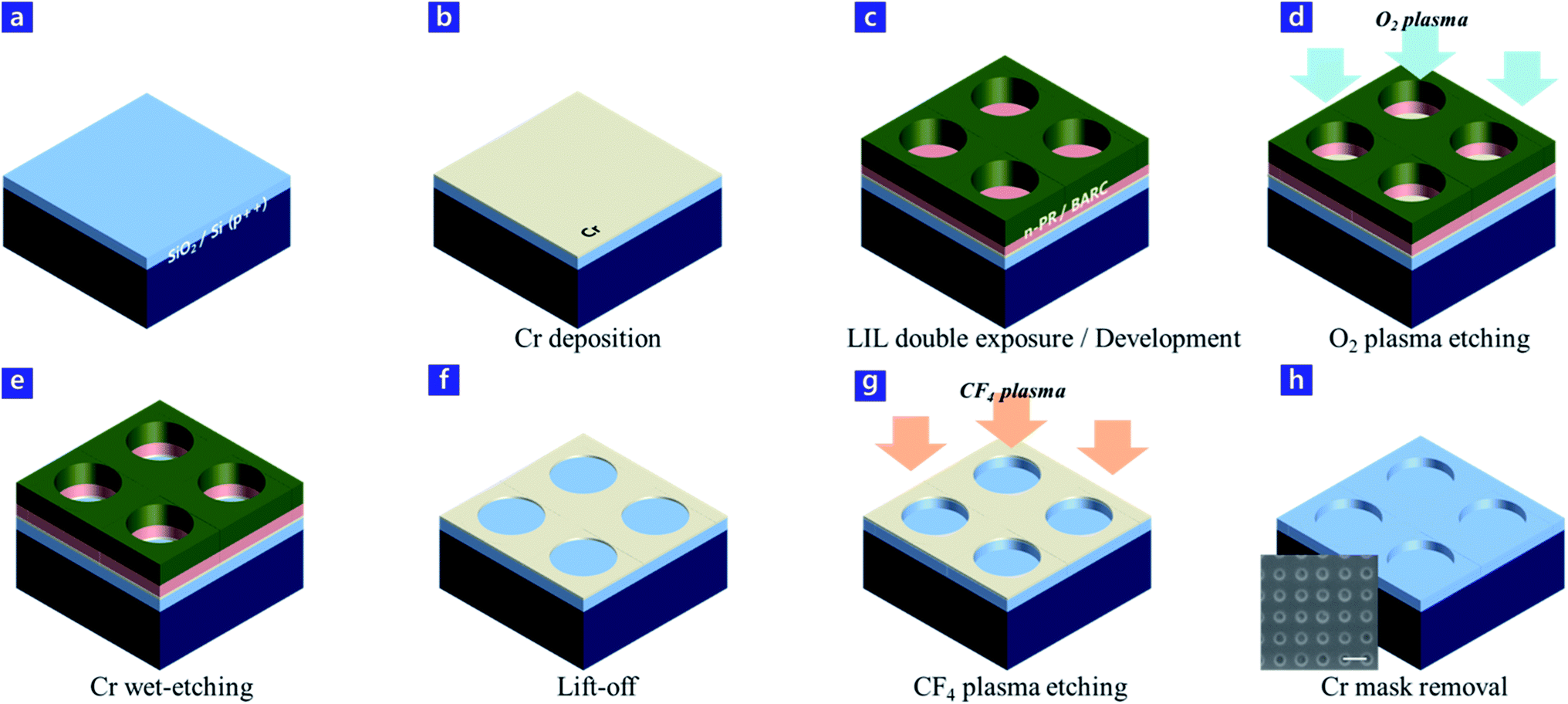 | ||
| Scheme 1 Fabrication of the NP SiO2/Si substrate: (a) cleaning of the SiO2/Si substrate, (b) deposition of a 10 nm thick Cr layer, (c) spin-coating of BARC and n-PR layers for laser interference lithography, followed by double exposure with a He–Cd laser (λ = 325 nm) and development process, resulting in the periodically aligned PR nanopores, (d) O2 plasma etching to eliminate the BARC and thus expose the underlying Cr layer within the nanopores, (e) Cr wet-etching within the nanopores, (f) removal of n-PR/BARC layers, leaving the Cr nanopore mask, (g) CF4 plasma etching to transfer the Cr mask pattern to the underlying SiO2 layer, and (h) removal of the Cr mask to produce the final product of the NP SiO2/Si substrate. The inset SEM image in (h) is the final SiO2/Si substrate having nanopores with a diameter of 442 nm at 1 μm pitch (scale bar: 1 μm). | ||
Fabrication of bottom-contact graphene field effect transistors (G-FETs)
Bottom-contact graphene field effect transistors (G-FETs) were fabricated. The bottom-contact structure was suggested to minimize the damage to the transferred graphene. First, source-drain electrodes, Au (50 nm)/Ti (10 nm), were defined on the substrate by photolithography with a channel length of 10 μm and a channel width of 50 μm. Afterward, single layer graphene (Graphene Square Inc., South Korea) was transferred onto the electrode-deposited substrate by the general wet-transfer technique.34 The transfer process is detailed in the ESI of S1.† The sample was then vacuum annealed at 300 °C for 1 h. This annealing process for removing the transfer polymer or other impurities was essential to explore the substrate-induced graphene doping and strain effects.35 Finally, a 30 nm Al2O3 layer was deposited on the whole sample as a passivation layer by atomic layer deposition (ALD) process.Measurement of the transfer characteristics (ID–VG curves)
The SiO2 layer was partially scratched out with a diamond cutter, and the exposed highly p-doped silicon was used as the back-gate contact. A Keithley 4200 system together with a probe-station (MST 5500B, MS TECH, South Korea) were utilized for measuring the transfer characteristics. The gate bias was introduced in the dual-sweep mode from −50 V to +50 V. All measurements were performed inside a nitrogen-purged glove box.Results and discussion
The schematic of the fabricated NP SiO2/Si substrate is shown in Fig. 1a. The periodically aligned nanopores with a diameter (d) at a pitch (p) were produced by a laser interference lithography (LIL, λ = 325 nm) process, which were controlled by several process parameters such as the Lloyd-mirror angle, laser exposure time and development time. The LIL system is further described in Fig. S2.† The pore height (h, 150 nm) was tuned by adjusting the plasma etching time with CF4 gas. Here, we fabricated NP SiO2/Si substrates with three different pitches at 500 nm, 1000 nm, and 1500 nm and three different pore diameters for each pitch. As the exposure time increased, the pore diameter decreased because a negative-tone photoresist (AZ nLOF 2020, MicroChemicals GmbH, Germany) was utilized, and thus, the porosity decreased.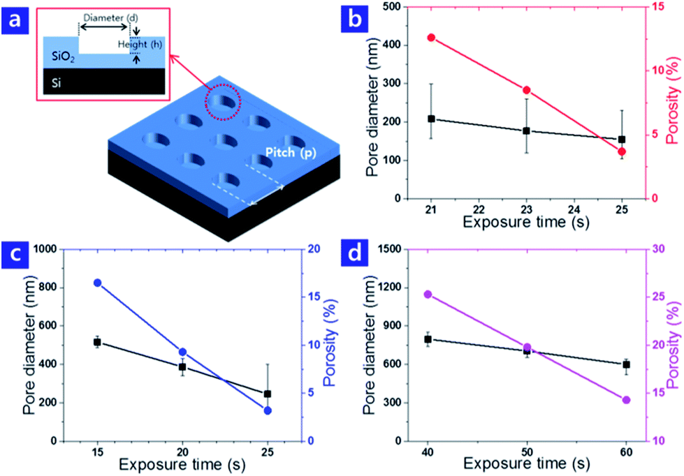 | ||
| Fig. 1 (a) Schematic of the NP SiO2/Si substrate. Pore diameter and porosity vs. exposure time at different pitches of (b) 500 nm, (c) 1000 nm, and (d) 1500 nm. The pitch was controlled by the interference angle between the two beams, and the pore diameter was determined by the exposure time and development time. All the samples were used as a gate dielectric layer for the following bottom-contact G-FETs. | ||
Commercially available single layer graphene (Graphene Square Inc., South Korea) was transferred onto the produced various NP SiO2/Si substrates by the wet-transfer technique.34 The obtained optical microscopic image shows that the transferred graphene was uniform and homogeneous without notable defects (Fig. 2a). Fig. 2b is a SEM image around the edge of the transferred graphene on the NP SiO2/Si substrate with aligned nanopores at a 1000 nm pitch. The graphene was suspended on the nanopores (red-dotted circle), which were blurred due to the graphene coverage. The schematic image is the vertical view of a nanopore that suspends the transferred graphene. In contrast, the nanopores without graphene coverage showed a clear appearance.
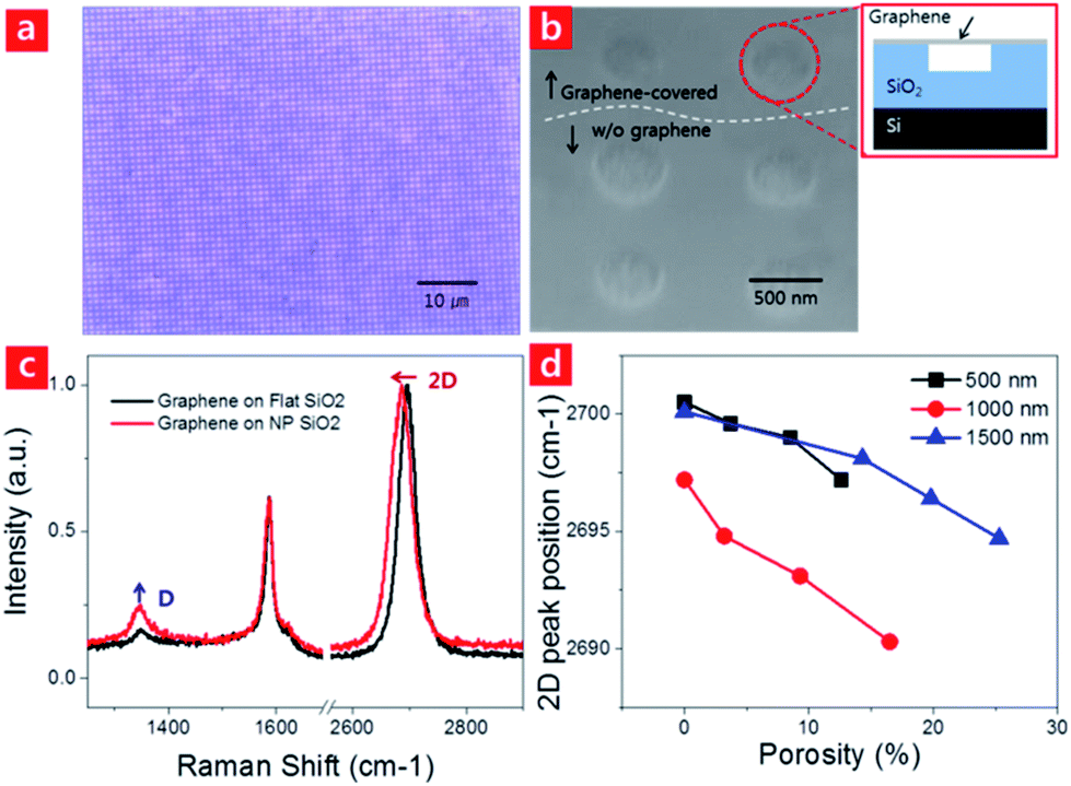 | ||
| Fig. 2 (a) An optical microscope image of the transferred graphene. (b) A SEM image of the edge of transferred graphene on the NP SiO2/Si substrate. The nanopore (red circle) was blurred with the suspended graphene. Meanwhile, the nanopores outside the graphene coverage looked clear. The schematic image depicts the suspended graphene on a nanopore. (c) Comparison of the Raman spectra of the transferred graphene on the flat and NP SiO2/Si substrates. (d) 2D peak shift in the Raman spectra of the transferred graphene vs. porosity of the NP SiO2/Si substrate at different pitches of 500 nm, 1000 nm, and 1500 nm. | ||
Raman spectroscopy was utilized to see the effect of annealing, and the effect of the pores of the underlying substrate on the graphene doping. It was reported that during the annealing process, tensile strain of graphene layer was switched to compressive strain, which was indicated by the red-shift of the Raman G- and 2D-peaks.36 Similar phenomena were occurred to our samples after heat-treatment even though the degree of red-shift was not large (see the ESI, S3†). Raman 2D-peaks mapping of the graphene on the flat- and NP substrates at 1 μm step in 10 × 10 μm2 area was also conducted before and after annealing process, indicating the less compressive strain of the suspended graphene on the nanopores (see the ESI, S4†). Fig. 2c compares the Raman spectra from the graphene transferred to flat and NP (d: 516 nm, p: 1000 nm) SiO2/Si substrates. In the case of the graphene transferred on the NP SiO2/Si substrate, the intensity of the D peak (∼1350 cm−1) increased compared to that for the flat SiO2/Si substrate. This could occur due to greater damage incurred during the graphene transfer onto the NP SiO2/Si substrate. Another noticeable difference between the two Raman spectra is that the 2D peak position (∼2700 cm−1) of the graphene transferred on the NP SiO2/Si substrate was relatively blue-shifted (from 2697 cm−1 to 2687 cm−1), signaling the relative n-doping phenomenon.
The graphene interfacing the oxygen (O)-terminated SiO2 substrate is known to be slightly p-doped by electron withdrawal from the graphene to the electronegative oxygen atom-terminated surface.37 In the case of the NP SiO2/Si substrate, when graphene was transferred onto the substrate, the graphene was partially suspended at the pores, inducing less interfacial area between them. Therefore, relative n-doping of the overlaid graphene could occur, considering the reduced interfacial area with the SiO2 layer. The 2D peak positions of the Raman spectra were examined with the transferred graphene on NP SiO2/Si substrates having three different porosities at a certain pitch (three different pitches in each pitch, total of 9 samples) to confirm the above hypothesis. Five points were measured in each sample. The Raman spectra from all the samples are shown in Fig. S5,† and the 2D peaks were collected to observe the doping tendency. At an identical pitch, as the porosity increased, the blue-shift degree of the 2D peak gradually increased, demonstrating the increment of the n-doping effect (Fig. 2d). Bottom-contact G-FETs were fabricated as shown in Fig. 3a to check the doping state of transferred graphene by measuring the Dirac voltage. Top-contact G-FETs were also prepared but, the underneath graphene was impaired during the source/drain electrode fabrication processes such as photolithography and the subsequent plasma etching. The top-contact G-FET made on the NP SiO2/Si substrates showed one order lower drain-current (ID) level, compared to that from the flat SiO2/Si substrate (Fig. S6†); this was possibly due to more severe damages because the partially suspended graphene was not fully supported by the substrate. With this reason, bottom-contact G-FET structure was adopted to minimize the process steps above graphene. After graphene transfer, an Al2O3 passivation layer (30 nm thick) was deposited by atomic layer deposition (ALD) to passivate the graphene layer from the ambient atmosphere. Fig. 3b shows a top-view SEM image of the G-FET as well as a magnified image of Al2O3/graphene on top of the NP substrate at the channel region. In addition, an image of the bare NP SiO2/Si substrate with the same magnification is inset for comparison. The Al2O3/graphene layer was suspended on the nanopores without noticeable breakages, and thus, the nanopores appeared to be blurred with the suspended layers. This was reconfirmed by the cross-sectional SEM image (Fig. 3c), indicating that the Al2O3/graphene layer was well suspended without sagging within the nanopore.
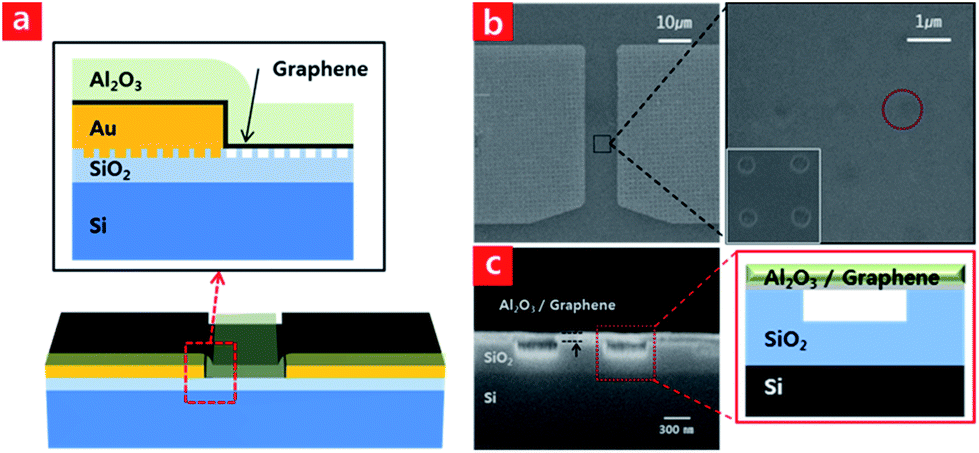 | ||
| Fig. 3 (a) A schematic of the bottom-contact G-FET fabricated on the NP SiO2/Si substrate. (b) A top-view SEM image of the G-FET on the NP SiO2/Si substrate. The channel region is magnified and compared with the inset image of the bare NP SiO2/Si substrate at the same magnification. The red circle indicates a vaguely seen nanopore on which the Al2O3/graphene layers is suspended. (c) A cross-sectional SEM image together with an equivalent schematic in the red square area, revealing that the suspended Al2O3/graphene layers were not sagging within the nanopore. | ||
Fig. 4 shows typical transfer curves of the G-FETs fabricated on the (a) flat and (b) NP SiO2/Si substrate. A NP SiO2/Si substrate with nanopores at a 1000 nm pitch with 15% porosity was used. Hereafter, we define the Dirac voltage as the gate voltage at which the drain current is at the minimum during the gate-voltage sweep, and the hysteresis as the difference between the two Dirac voltages in forward and backward sweeps. In the case of flat SiO2/Si substrate, the Dirac voltages in forward and backward sweeps were nearly same independent of the drain voltages (VD), and therefore, the hysteresis was minimal as shown in Fig. 4a. In contrast, in the case of NP SiO2/Si substrate, the Dirac voltages in both sweeps were much different, leading to enlarged hysteresis, as shown in Fig. 4b.
 | ||
| Fig. 4 Transfer characteristics (VG–ID curves) of the G-FETs produced on the (a) flat- and (b) NP SiO2/Si substrate. The gate voltage (VG) was dual-swept from −50 V to +50 V at different drain voltages (0.1 V, 0.3 V, and 0.5 V). | ||
Table 1 summarizes the Dirac voltages and the hysteresises extracted from all transfer curves measured at different VD of 0.1 V, 0.3 V, and 0.5 V. In the case of NP SiO2/Si substrate, as the VD increased, the Dirac voltage in backward sweep shifted from −9 V to −7 V along with the increased hysteresis from 8 V to 10 V. It is reported that the hysteresis was mainly attributed to the H2O and O2 molecules trapped on graphene, generating OH− ions on the graphene (eqn (1)).38
| O2 + 2H2O + 4e− (graphene) → 4OH− | (1) |
| VD [V] | Flat SiO2/Si substrate | NP SiO2/Si substrate | ||||
|---|---|---|---|---|---|---|
| FS | BS | Hysteresis | FS | BS | Hysteresis | |
| FS: forward sweep (−50 → +50 V), BS: backward sweep (+50 → −50 V). | ||||||
| 0.1 | −3 | 0 | 3 | −17 | −9 | 8 |
| 0.3 | −3 | 0 | 3 | −17 | −8 | 9 |
| 0.5 | −3 | 0 | 3 | −17 | −7 | 10 |
In the forward sweep, when a gate voltage is positively biased, these OH− ions are accumulated at the interface between the SiO2 surface and the overlaid graphene owing to electrostatic effect, which partially screen the electric field between the gate electrode and the graphene in the following backward sweep. Thus, a higher gate voltage was required for the Fermi level to be aligned with the Dirac point, transiently shifting the Dirac voltage to the p-doping direction compared to that of forward sweep.38 In the case of the NP SiO2/Si substrate, there are many nanopores that could trap more H2O and O2 molecules, inducing the larger hysteresis. In addition, the plasma-etching process used to make the nanopores generated a rougher surface that could supply more trap sites.
It is notable that the Dirac voltage of the NP SiO2/Si substrate in the forward sweep shifted to a much more negative voltage (−17 V), compared to the −3 V of the flat SiO2/Si substrate. This large relative n-doping could not be explained by the contact doping effect only. Rather, this phenomenon can be explained by the electrostatic doping effect originated from the difference in the capacitance of dielectric layer. Fig. 5 shows the schematics of the dielectric layer of the two cases and their equivalent capacitance circuits for the (a) flat and (b) NP SiO2/Si substrates. For the general metal–insulator–metal (MIM) capacitor structure, the capacitance (C) is generally expressed by eqn (2);
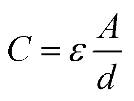 | (2) |
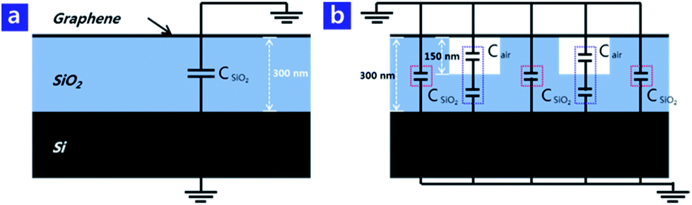 | ||
| Fig. 5 Schematic of the cross-sectional dielectric layers along with their equivalent capacitor circuits for the (a) flat SiO2/Si substrate and (b) NP SiO2/Si substrate. | ||
Here, ε, A, and d are the permittivity of the dielectric material, the overlapped area of the two plates, and the separation between the plates, respectively. For the flat SiO2/Si substrate, the capacitance is simply expressed as the overlapped equivalent capacitor circuit, as shown in Fig. 5a. For the NP SiO2/Si substrate, it is complicated to calculate the capacitance because the total capacitance consists of two kinds of capacitances, as depicted in Fig. 5b. The first one is the 300 nm-thick SiO2 capacitance from the areas of supported graphene (red dotted rectangles), and the second is the capacitance from the areas of suspended graphene (blue dotted rectangles within the nanopores) in which the 150 nm-thick SiO2 capacitance is serially connected to the 150 nm-thick air capacitances (SiO2–air hetero-structured dielectric layer). Overall, these two capacitances are connected in parallel. The capacitance of the 300 nm-thick SiO2 is known to be 11.6 nF cm−2.39 From this value, the capacitances of the 150 nm-thick SiO2 and the 150 nm-thick air were calculated as 23.2 nF cm−2, and 5.9 nF cm−2, respectively, by using εair = 1.0 and εSiO2 = 3.9.
The capacitance calculation for the NP SiO2/Si case is complicated and detailed in the ESI of S7.† Although it appears that many capacitances (all belonging to one of the two capacitance types) are connected in parallel to each other, the capacitance can be calculated simply by adding the two types of capacitances (calculated per unit area of cm2) multiplied by the respective porous (i.e., suspended graphene) and non-porous (i.e., supported graphene) area fractions; the calculated capacitances of the different samples having different pitch and porosity are listed in Table 2. Compared to the capacitance of the flat SiO2/Si substrate (11.6 nF cm−2), the calculated capacitances of the NP SiO2/Si substrates are relatively low. Therefore, even though the same gate bias was introduced, the induced electric field to the graphene channel through the dielectric layer was lowered by the lower capacitance of the dielectric layer compared to that of the flat substrate. Consequently, in the case of NP G-FET, the Dirac voltage shifted to a more negative value than that of the flat G-FET to compensate for the reduced capacitance.
| Flat | Pitch: 1500 nm | |||||
|---|---|---|---|---|---|---|
| Porosity [%] | 0 | 9.6 | 15.0 | 21.7 | ||
| Cap. [nF cm−2] | 11.6 | 10.94 | 10.57 | 10.11 | ||
| Pitch: 1000 nm | Pitch: 500 nm | |||||
|---|---|---|---|---|---|---|
| Porosity [%] | 9.9 | 13.9 | 25.0 | 2.0 | 4.1 | 20.8 |
| Cap. [nF cm−2] | 10.92 | 10.65 | 9.89 | 11.46 | 11.32 | 10.17 |
G-FETs were fabricated on the flat SiO2/Si substrate and on nine different NP SiO2/Si substrates, as depicted in Fig. 1, to examine the effects of porosity and pitch on the Dirac voltage shift. Fig. 6a shows the representative transfer curves (zoomed in around the Dirac voltage) of the G-FETs fabricated on the 500 nm-pitch NP SiO2/Si substrates with different porosities. The arrows indicate the Dirac voltages; black for the forward sweep and red for the backward sweep. Normally p-typed graphene became n-type when being contacted with the 500 nm-pitch NP SiO2/Si substrate at 2% porosity. As the porosity increased, the Dirac voltage shifted to more negative value (Fig. 6b). The capacitance of the dielectric layer was reduced with increasing porosity (Table 2), leading to the Dirac voltage shift to more negative value to compensate for the reduced capacitance, as discussed in Fig. 5.
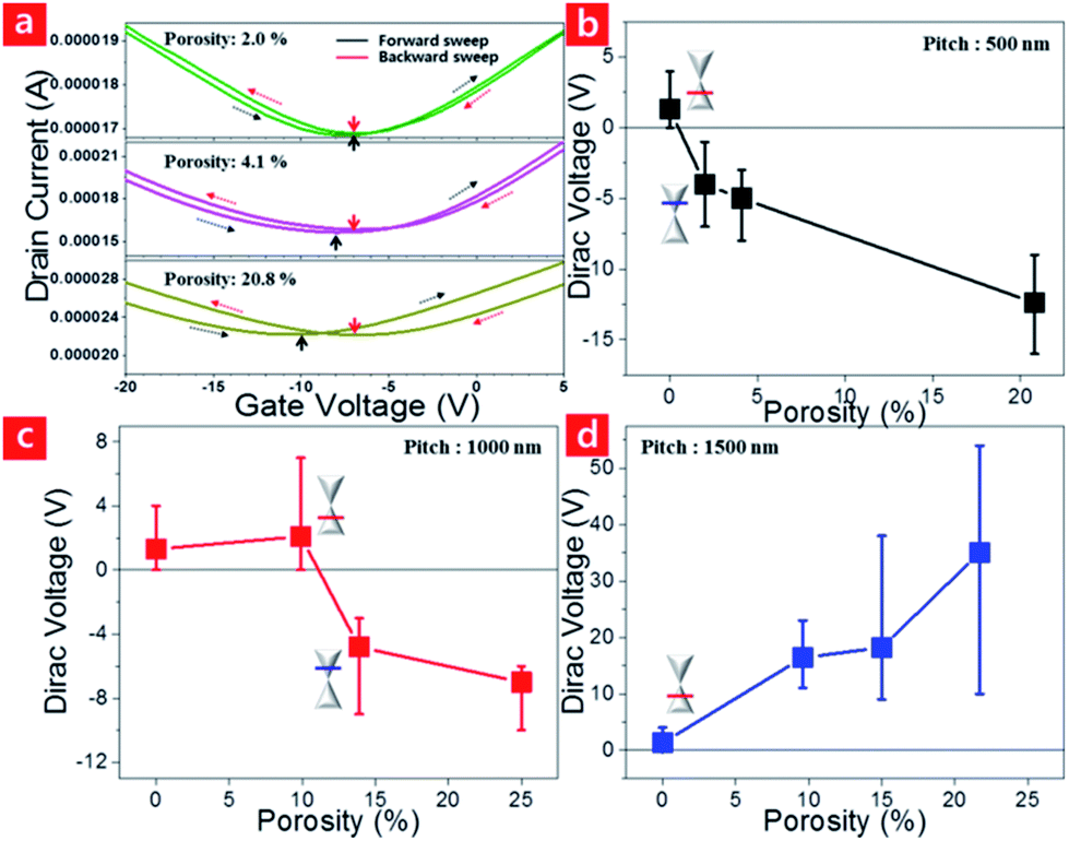 | ||
| Fig. 6 (a) Comparison of the transfer curves (zoomed in around the Dirac voltage) of the G-FETs on the NP SiO2/Si substrate at a pitch of 500 nm; the arrows indicate the Dirac voltages during the forward- (black) and backward sweep (red). The Dirac voltage shift vs. different porosities at a pitch of (b) 500 nm, (c) 1000 nm, and (d) 1500 nm. | ||
The transfer curves from the NP G-FETs with different porosities at 1000 nm- and 1500 nm pitches are shown in Fig. S8,† and the Dirac voltage shift with increasing porosity is plotted in Fig. 6c and d, respectively. Interestingly, for the case of the 1500 nm pitch, the Dirac voltage shifted to more positive value with increasing porosity (Fig. 6d), which is opposite to the case of the 500 nm pitch. We found that the direction of the Dirac voltage shift was mainly dependent on the initial doping polarity of the graphene (whether p-type or n-type) by the substrate-induced contact-doping. As discussed in the Raman spectra results (Fig. 2c and d), the graphene on the NP SiO2/Si substrate demonstrated relative n-doping properties compared to the flat SiO2/Si substrate's case. If the graphene was initially n-type after contacting to the underneath substrate, the Dirac voltage shifted to a more negative value with increasing porosity, as in the case of 500 nm (Fig. 6b). If the graphene was initially p-type, on the other hand, the Dirac voltage shifted to a more positive value with increasing porosity, as in the case of 1500 nm (Fig. 6d).
In the case of 1000 nm pitch, the doping polarity switched at a certain porosity between 9.9% and 13.9%, meaning that the transferred graphene was still p-type when it was contacted to the SiO2/Si substrate with the porosity below 9.9% and became n-type on top of the substrate having a porosity above 13.9% (Fig. 6c). Depending on the initial graphene doping polarity, different Dirac voltage shift was demonstrated with increasing the porosity; to a higher (positive) voltage up to 9.9% porosity with the initially p-type graphene or to a lower (negative) voltage above 13.9% porosity with the initially n-type graphene. This result indicates that the initial graphene doping type can be modulated by the porosity of the underlying substrate.
Fig. 7a shows the effect of porosity on the hysteresis. At an identical pitch, an increase in porosity means that larger pores support the graphene layer, which could trap more H2O and O2 molecules, and thus generate more OH− ions, leading to a larger hysteresis, as shown in Fig. 7a. In addition, three samples with similar porosities were selected from each pitch to evaluate the pitch size effect on the hysteresis (Fig. 7b). In this case, a decrease in the pitch means that a graphene layer is suspended on highly dense nanopores with a smaller pore size. Therefore, a smaller amount of H2O or O2 molecules can be trapped inside the pores, inducing the reduced hysteresis with decreasing pitch size.
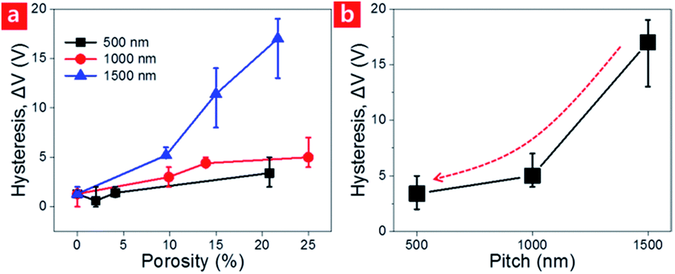 | ||
| Fig. 7 (a) Hysteresis variation of the G-FETs on the NP SiO2/Si substrates with different porosities at a fixed pitch. (b) Hysteresis variation of the G-FETs on the NP SiO2/Si substrates with different pitches, having similar porosities of 20.8%, 25%, and 21.7% for the 500 nm, 1000 nm, and 1500 nm pitch, respectively. | ||
Conclusions
Substrate-induced doping effects were investigated with G-FETs fabricated on size- and pitch-tunable NP SiO2/Si substrates. The graphene transferred onto the NP SiO2/Si substrate was partially suspended on the nanopores and demonstrated relative n-doping properties compared to the transferred graphene on a flat SiO2/Si substrate. The dielectric layer composed of the periodically aligned nanopores had a relatively lower capacitance than that of the flat SiO2/Si substrate. The initial doping type of graphene was determined by the pore geometry on which the graphene was transferred. As the porosity increased, the Dirac voltage shifted to a higher positive or lower negative value, depending on the initial graphene doping polarity (p- or n-type, respectively). The degree of graphene doping was affected by the combination of the contact and electrostatic effects. The NP SiO2/Si substrate with smaller nanopores demonstrated a reduced hysteresis due to the smaller amount of H2O or O2 molecules trapped within the smaller pores.This newly developed substrate-induced graphene doping technique has its worth in that graphene doping type can be effectively tuned by the nanopore geometry of the underlying substrate without additional dopants. This doping technique can also be applied to other two-dimensional (2D) materials, such as molybdenum disulfide (MoS2), tungsten disulfide (WS2), and tungsten diselenide (WSe2) for various applications.
Conflicts of interest
There are no conflicts to declare.Acknowledgements
This work was supported by the Pioneer Research Center Program (NRF-2016M3C1A3908893) and by the Basic Science Research Program (NRF-2016R1A2B4006395) through the National Research Foundation of Korea (NRF) funded by the Ministry of Education. The research was partially supported by the GIST Research Institute (GRI) project through a grant provided by GIST in 2017.Notes and references
- K. S. Novoselov, A. K. Geim, S. V. Morozov, D. Jiang, Y. Zhang, S. V. Dubonos, I. V. Grigorieva and A. A. Firsov, Science, 2004, 306, 666 CrossRef CAS PubMed.
- K. I Bolotin, K. J. Sikes, Z. Jiang, M. Klima, G. Fudenberg, J. Hone, P. Kim and H. L. Stormer, Solid State Commun., 2008, 146, 351 CrossRef.
- L. A. Jauregui, Y. Yue, A. N. Sidorov, J. Hu, Q. Yu, G. Lopez, R. Jalilian, D. K. Benjamin, D. A. Delk, W. Wu, Z. Liu, X. Wang, Z. Jiang, X. Ruan, J. Bao, S. S. Pei and Y. P. Chen, ECS Trans., 2010, 28, 73 CAS.
- C. Lee, X. Wei, J. W. Kysar and J. Hone, Science, 2008, 321, 385 CrossRef CAS PubMed.
- R. R. Nair, P. Blake, A. N. Grigorenko, K. S. Novoselov, T. J. Booth, T. Stauber, N. M. R. Peres and A. K. Geim, Science, 2008, 320, 1308 CrossRef CAS PubMed.
- K. F. Mak, L. Ju, F. Wang and T. F. Heinz, Solid State Commun., 2012, 152, 1341 CrossRef CAS.
- F. Xia, T. Mueller, Y. Lin, A. Valdes-Garcia and P. Avouris, Nat. Nanotechnol., 2009, 4, 839 CrossRef CAS PubMed.
- C. Liu, Y. Chang, T. B. Norris and Z. Zhong, Nat. Nanotechnol., 2014, 9, 273 CrossRef CAS PubMed.
- X. Xu, N. M. Gabor, J. S. Alden, A. M. Zande and P. L. McEuen, Nano Lett., 2010, 10, 562 CrossRef CAS PubMed.
- F. Xia, U. Yan and P. Avouris, Proc. IEEE, 2013, 101, 1717 CrossRef CAS.
- A. K. Geim and K. S. Novoselov, Nat. Mater., 2007, 6, 183 CrossRef CAS PubMed.
- A. K. Geim, Science, 2009, 324, 1530 CrossRef CAS PubMed.
- S. Pang, Y. Hernandez, X. Feng and K. Mullen, Adv. Mater., 2011, 23, 2779 CrossRef CAS PubMed.
- Y. Xu and J. Liu, Small, 2016, 12, 1400 CrossRef CAS PubMed.
- J. Meng, H. Song, C. Li, Y. Jin, L. Tang, D. Liu, Z. Liao, F. Xiu and D. Yu, Nanoscale, 2015, 7, 11611 RSC.
- T. H. Bointon, G. F. Jones, A. D. Sanctis, R. H. Pearce, M. F. Craciun and S. Russo, Sci. Rep., 2015, 5, 16464 CrossRef CAS PubMed.
- B. Guo, L. Fang, B. Zhang and J. R. Gong, Insci. J., 2011, 1, 80 CrossRef CAS.
- H. Liu, Y. Liu and D. Zhu, J. Mater. Chem., 2011, 21, 3335 RSC.
- R. Beams, L. G. Cancado and L. Novotny, J. Phys.: Condens. Matter, 2015, 27, 083002 CrossRef PubMed.
- C. Stampfer, F. Molitor, D. Graf, K. Ensslin, A. Jungen and C. H. Wirtz, Appl. Phys. Lett., 2007, 91, 241907 CrossRef.
- C. Casiraghi, S. Pisana, K. S. Novoselov, A. K. Geim and A. C. Ferrari, Appl. Phys. Lett., 2007, 91, 233108 CrossRef.
- P. A. Khomyakov, G. Giovannetti, P. C. Rusu, G. Brocks, J. Brink and P. J. Kelly, Phys. Rev. B, 2009, 79, 195425 CrossRef.
- G. Giovannetti, P. A. Khomyakov, G. Brocks, V. M. Karpan, J. Brink and P. J. Kelly, Phys. Rev. Lett., 2008, 101, 026803 CrossRef CAS PubMed.
- W. X. Wang, S. H. Liang, T. Yu, D. H. Li, Y. B. Li and X. F. Han, J. Appl. Phys., 2011, 109, 07C501 CrossRef.
- A. Kasry, M. A. Kuroda, G. J. Martyna, G. S. Tulevski and A. A. Bol, ACS Nano, 2010, 4, 3839 CrossRef CAS PubMed.
- J. Oh, K. Kim and G. Yeom, J. Nanosci. Nanotechnol., 2014, 14, 1120 CrossRef CAS PubMed.
- J. Shim, C. H. Lui, T. Y. Ko, Y. Yu, P. Kim, T. R. Heinz and S. Ryu, Nano Lett., 2012, 12, 648 CrossRef CAS PubMed.
- H. E. Romero, P. Joshi, A. K. Gupta, H. R. Gutierrez, M. W. Cole, S. A. Tadigadapa and P. C. Eklund, Nanotechnology, 2009, 20, 245501 CrossRef PubMed.
- F. Schedin, A. K. Geim, S. V. Morozov, E. W. Hill, P. Blake, M. I. Katsnelson and K. S. Novoselov, Nat. Mater., 2007, 6, 652 CrossRef CAS PubMed.
- E. H. Hwang, S. Adam and S. D. Sarma, Phys. Rev. B, 2007, 76, 195421 CrossRef.
- T. O. Wehling, K. S. Novoselov, S. V. Morozov, E. E. Vdovin, M. I. Katsnelson, A. K. Geim and A. I. Lichtenstein, Nano Lett., 2008, 8, 173 CrossRef CAS PubMed.
- D. Wei, Y. Liu, Y. Wang, H. Zhang, L. Huang and G. Yu, Nano Lett., 2009, 9, 1752 CrossRef CAS PubMed.
- H. Liu, Y. Liu and D. Zhu, J. Mater. Chem., 2011, 21, 3335 RSC.
- A. Reina, X. Jia, J. Ho, D. Nezich, H. Son, V. Bulovic, M. S. Dresselhaus and J. Kong, Nano Lett., 2009, 9, 30 CrossRef CAS PubMed.
- S. Costa, J. Weis, O. Frank, M. Fridrichova and M. Kalbac, RSC Adv., 2016, 6, 72859 RSC.
- J. Lee, G. Ahn, J. Shim, Y. Lee and S. Ryu, Nat. Commun., 2012, 3, 1024 CrossRef PubMed.
- Y. Kang, J. Kang and K. J. Chang, Phys. Rev. B: Condens. Matter Mater. Phys., 2008, 78, 115404 CrossRef.
- L. Zheng, X. Cheng, D. Cao, Z. Wang, C. Xia, Y. Yu and D. Shen, Appl. Phys. Lett., 2014, 104, 023112 CrossRef.
- Y. M. Lin, H. Y. Chiu, K. A. Jenkins, D. B. Farmer, P. Avouris and A. Valdes-Garcia, IEEE Electron Device Lett., 2010, 31, 68 CrossRef CAS.
Footnotes |
| † Electronic supplementary information (ESI) available. See DOI: 10.1039/c7ra11601b |
| ‡ The authors equally contributed to this work. |
| This journal is © The Royal Society of Chemistry 2018 |