
 Open Access Article
 This Open Access Article is licensed under a
 Creative Commons Attribution 3.0 Unported Licence
Mechanical switching in ferroelectrics by shear stress and its implications on charged domain wall generation and vortex memory devices
W. J. Chen abd,
Shuai Yuanbc,
L. L. Mabc,
Ye Jiab,
Biao Wangd and
Yue Zheng*ab
abd,
Shuai Yuanbc,
L. L. Mabc,
Ye Jiab,
Biao Wangd and
Yue Zheng*ab
aState Key Laboratory of Optoelectronic Materials and Technologies, Sun Yat-sen University, Guangzhou, 510275, China. E-mail: zhengy35@mail.sysu.edu.cn; Tel: +86-20-84113231
bMicro & Nano Physics and Mechanics Research Laboratory, School of Physics, Sun Yat-sen University, Guangzhou, 510275, China
cSchool of Engineering, Sun Yat-sen University, Guangzhou, 510275, China
dSino-French Institute of Nuclear Engineering and Technology, Sun Yat-sen University, Zhuhai, 519082, China
First published on 24th January 2018
Abstract
Recently, the resurgence of interest in flexoelectricity in solids has promoted research on switching of ferroelectric domains via mechanical loads. In this work, combining thermodynamic calculation and phase-field simulation, we revealed that mechanical switching of polarization can be achieved in ferroelectrics by shear stress via a simple mechanism where the presence of flexoelectricity is not necessary. The switching is a consequence of the trilinear coupling between shear stress and the two polarization components that lie in the shear strain plane. Specifically, when the direction of one polarization component is fixed, switching of the other component can be induced by applying a shear stress. Moreover, when the shear stress is fixed, switching of one of the polarization components can lead to the switching of the other component. Phase diagrams of the stable polarization state as a function of shear stress, temperature and electric field are calculated. Furthermore, as demonstrated by phase-field simulation on a ferroelectric thin film, domain switching can indeed be realized by a local shear stress. Importantly, the combining effect of shear stress and electric field can lead to a deterministic writing of charged domain walls, which should be very useful for the fabrication of domain wall devices. The implication of such a shear-stress-modified polarization switching on the design of vortex memory device is also discussed.
Introduction
‘Ferroelectrics’ refers to a class of materials that exhibit a spontaneous polarization P below a temperature point and P is switchable under an electric field E. This attribute makes them promising in developing nonvolatile memory devices.1 Ferroelectrics also have wonderful applications such as in sensors,2 actuators,3 energy conversion/storage devices,4–6 optical switches,7 microwave devices,8 etc., due to a wide spectrum of other functional properties including piezoelectricity, pyroelectricity, electro-optic effects, and nonlinear dielectric/optic behavior. Importantly, the properties of ferroelectrics generally exhibit dependence on the polarization state and the domain structure, and it is well-known that the polarization state and the domain structure of ferroelectrics are strongly coupled to external thermal, electrical and mechanical fields.9–11 These features indicate abundant controllability of ferroelectric devices via domain engineering.Due to the direct coupling between polarization P and electric field E, it is natural to manipulate (e.g., switch, reorient or erase) ferroelectric domains electrically. As the applied field is required to be larger than the coercive field, which is usually in order of 107 to 108 V m−1, electric-field-driven processes such as charge injection (extraction) from (into) the electrode, electrochemical process near the electrode/ferroelectric interface, and charged defect migration can be quite significant. While it is still under debate, the injected charges or mobile defects are believed to be captured by the interface (and form a space charge layer which decreases the effective field applied and depresses domain inversion) or by the charged domain walls that appear during domain switching (and consequently pin the domain walls and depresses domain inversion). As a consequence, fatigue problem is quite difficult to avoid.12,13 While internal electric field might also play an important role, fatigue problem, at least the contribution from charge injection, is expected to be largely eased if external electric field is absent. Electrical switching also causes complex memristive dynamics,14,15 leakage and even dielectric break-down problem. It is therefore desirable to identify possible effects that can facilitate domain switching and alternative switching strategies using nonelectrical fields.
Most ferroelectric phase transition behaviors are caused by the collective lattice distortions. Consequently, ferroelectric polarization is intrinsically coupled with stress and strain fields. However, it is not a common idea to apply mechanical fields to switch ferroelectric domains. This is because stress σ or strain ε is coupled with ferroelectric polarization P in an even symmetry, i.e., −σP2 or −εP2. The switching of P to −P would not change the system's energy. Nevertheless, it should be pointed out that this argument is only applicable to perfect 180° switching and to homogeneous system. On the one hand, it is well-known that ferroelectric domains can be reoriented by strain or stress, such as strain-induced transformation from a domain to c domain in a ferroelastic domain pattern. On the other hand, when the system is inhomogeneous, e.g., subjected to inhomogeneous stress/strain state, or with surfaces/interfaces, other effects can enter into the role in facilitating mechanical switching of ferroelectric domains. For example, it has been realized that strain gradient can lead to 180° switching of polarization in a similar way of electric field, namely flexoelectricity. This is because strain gradient is an odd-parity tensor without inversion symmetry, similar to an electric field.
Recently, notable progresses have been achieved in issue of mechanical switching of ferroelectric domains.16–30 On the experimental front, Lu et al.16 for the first time demonstrated that the stress gradient generated by the tip of an atomic force microscope (AFM) can switch the polarization locally in BaTiO3 (BTO) thin film. Afterwards, a number of works have been performed, demonstrating the feasibility of mechanical switching in ferroelectric polymer films,17,18 thick films,19 multiferroic thin films,20,21 semiconducting films,22 etc. The effects of substrate misfit strain23,24 and loading mode (i.e., perpendicular mechanical load vs. sliding load)25 on the mechanical switching behavior, and the asymmetric feature of mechanical switching in the vicinity of an existing domain wall,26 have been explored. On the theoretical aspect, a number of works based on methods such as finite element simulations,16,25 molecular dynamics simulation,26 phase-field method,27–29 first-principles calculation,30 etc., have also been performed to gain a deep insight into the mechanism of mechanical switching. It should be pointed out that previous works mainly focused on mechanical switching in thin films under perpendicular tip-loading mode or bending mode, where flexoelectric field due to the transverse and longitudinal strain/stress gradients is believed to be important. In such cases, the shear strain/stress gradient is at least an order smaller in magnitude and its influence is negligible. As two exceptional cases, Očenášek et al.25 have shown that shear strain gradient can play a dominant role over compressive strain gradient in the flexoelectric domain switching process under sliding loading mode; Li et al.30 have studied the shear strain gradient effect on the polarization reversal of BTO thin films. Also noteworthy is that, for systems with surfaces or interfaces, other effects beyond flexoelectricity such as surface piezoelectricity,31 interfacial bonding and screening effect,32,33 contact electrification,34 and surface electrochemical process35 are possible to be modified by mechanical fields to facilitate mechanical switching of ferroelectric domain. For example, a recent work has shown that mechanical switching driven by depolarization field can be achieved in ferroelectric thin films, with both up-to-down and down-to-up switching modes and a hidden nonlocal switching mode.33 Considering the controversy in the literature on the magnitude of flexoelectric coefficients and many other possible sources that may affect domain switching, it is of significance to reveal other possible mechanical switching mechanisms.
In this work, based on thermodynamic calculation and phase-field simulation, we showed an overlooked mechanism of mechanical switching of polarization in BTO via shear stress engineering. In this mechanism, the trilinear coupling between shear stress and the two polarization components that lie in the shear strain plane is exploited, and the presence of flexoelectricity is not necessary. Specifically, when the direction of one polarization component is fixed, switching of the other component can be induced by applying a shear stress. Moreover, when the shear stress is fixed, switching of one of the polarization components can lead to the switching of the other component. The stable polarization state as a function of shear stress, temperature and electric field is calculated. Phase-field simulation is then performed to verify the shear-stress-induced domain switching in ferroelectric thin film. Besides the normal switching where neutral domain walls are involved, a deterministic writing of charged domain walls can be also achieved via the combining application of shear stress and electric field. This should be very useful for the fabrication of domain wall devices. At the end, we discuss that such a shear-stress-modified polarization switching can provide us a novel design of vortex memory device.
Model and methodology
Thermodynamic model
We model the thermodynamics of ferroelectrics based on the phenomenological Landau–Devonshire theory. The quantities such as polarization and stress are described in a Cartesian coordinate system (Fig. 1a). To consider the response of a thermodynamic system in response to external stress and electric field, here we adopt the Gibbs free energy. Taking the state of the paraelectric crystal at zero stress and electric field as the reference, the free energy density of a ferroelectric crystal as a function of polarization, stress and electric field is written as,36
 | (1) |
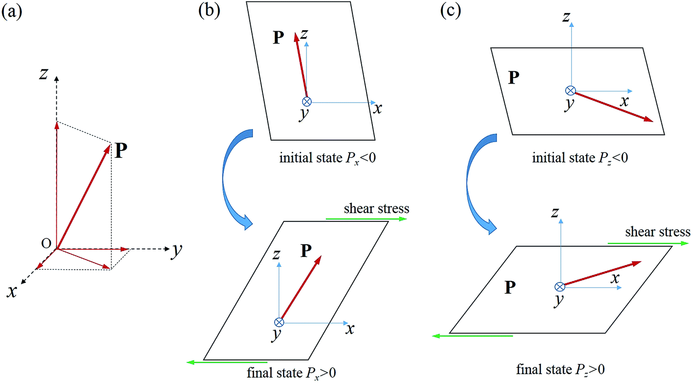 | ||
| Fig. 1 (a) Schematic of a polarization vector in a Cartesian coordinate system. (b and c) Schematic of two possible switching behaviors of a polarization vector (Px, Pz) by shear stress σzx. (b) Switching from (Px, Pz) into (−Px, Pz), and (c) switching from (Px, Pz) into (Px, −Pz). | ||
For BTO, an eight-order Landau–Devonshire potential is usually employed.37 For simplicity, we consider that the BTO crystal is subjected to a uniform shear stress σzx, and an external electric field along the z-axis Ez. The explicit expression of the free energy density is then given by
 | (2) |
It can be seen from eqn (2) that the two polarization components, Px and Pz, and the shear stress σzx are coupled with each other in a trilinear form 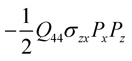 . This coupling term, together with the last term, −EzPz, enforces a condition of the sign of these three quantities. The other terms of the free energy density do not depend on the signs of Px, Pz, and σzx. That is to say, once the signs of two of them are fixed, the sign of the third one cannot change arbitrarily, as required by the energy minimum principle. This condition provides us the mechanism of polarization switching by shear stress as schematically shown in Fig. 1b. Specifically, two possible switching behaviors of a polarization vector (Px, Pz) can be expected, depending on the relative stability of the two polarization components. In the first case, the polarization component Pz is more stable, and the application of shear stress σzx leads to the switching of Px. In the second case, the polarization component Px is more stable, and the application of shear stress σzx leads to the switching of Pz. Note that it is the trilinear term that determines the relative signs of Px, Pz, and σzx, as it is the only term that links the three quantities, meanwhile the relative stability of the two polarization components can be modified by external electric field via the last term. Other factors, such as temperature, misfit strain, screening condition, etc., can also modify the relative stability of the two polarization components.
The equilibrium polarization state can be obtained by minimizing the free energy density G in eqn (2), ∂G/∂Pi = 0, i.e.,
 | (3a) |
 | (3b) |
 | (3c) |
The application of shear stress σzx and electric field Ez lowers the degeneracy of the ferroelectric phases of BTO. To classify the different phases, we introduce the following notations: (i) the c-phase, where Px = Py = 0 and Pz ≠ 0; (ii) the O-phase, where |Px| = |Pz| ≠ 0 and Py = 0; (iii) the r1-phase, where |Px| = |Py| = |Pz| ≠ 0; (iv) the r2-phase, where Px = −Pz ≠ 0, and Py ≠ 0; (v) the r3-phase, where Px = Pz ≠ 0, and Py ≠ 0; (vi) the ac1-phase, where |Px| ≠ |Pz|, PxPz < 0 and Py = 0; (vii) the ac2-phase, where Px = −Pz ≠ 0 and Py = 0; (viii) the ac3-phase, where |Px| ≠ |Pz|, PxPz > 0 and Py = 0; and (ix) the ac4-phase, where Px = Pz ≠ 0 and Py = 0. Values of expansion coefficients of the eight-order approximated potential for BTO are from ref. 37, and those of the electrostrictive coefficients and the elastic compliance coefficients are from ref. 38.
Phase-field simulation
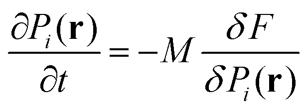
We construct a phase-field model to investigate the domain switching behavior of BTO thin film subjected to a local shear stress. In this model, the temporal evolution of the spontaneous polarization field is described by the time-dependent Ginzburg–Landau (TDGL) equations,
 | (4) |
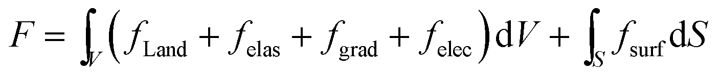
The total free energy is a sum of the Landau free energy FLand, elastic energy Felas, gradient energy Fgrad, electrostatic energy Felec and surface energy Fsurf, that is,
 | (5) |
The Landau energy density fLand is taken to be at zero stress and zero electric field, that is, the one given in eqn (2) with the elastic and the electric terms excluded. Under the condition of applied stress, the mechanical stress field (applied and internal) and its coupling with the polarization field contribute to the elastic energy density, which is given by,
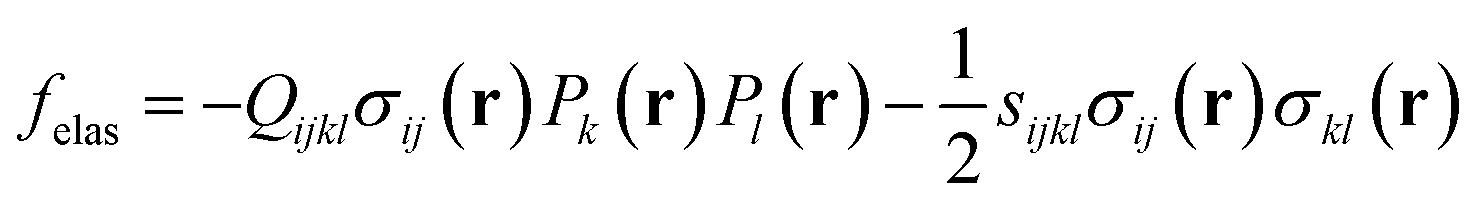 | (6) |
In the absence of body forces, the inhomogeneous stress field σij(r) is calculated by solving the mechanical equilibrium equation, i.e., σij,j(r) = 0, where the comma in the subscript denotes spatial differentiation. Here the thin film is assumed to be epitaxially grown on an elastic substrate. The film/substrate system is subjected to the contact force of an AFM tip with a trend of relative motion along the film surface. The mechanical boundary at the top surface is given by niσik = τk, where τk is the local surface traction caused by the tip force and ni is the ith component of the unit vector normal to the surface. Specifically, the local surface traction consists of a normal component τz and a lateral component τx, corresponding to a compression force Fp and a friction force Ff, respectively. In calculating the stress field, a thick-enough layer of substrate is included and the bottom boundary of the film/substrate system is fixed in displacement. For simplicity, the elastic property of the substrate is taken to be the same with that of the ferroelectric thin film.
The gradient energy, or called domain wall energy, is caused by the inhomogeneity of the polarization field. For a perovskite ferroelectric such as BTO, to the lowest order of the Taylor expansion, the gradient energy density takes the form as
 | (7) |
 are gradient energy coefficients, and Pi,j denotes the derivative of the ith component of the polarization vector, Pi, with respect to the jth coordinate.
The electric energy density of a given polarization distribution is given by
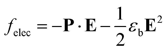 | (8) |
| Di,i = (εbE + P)i,i = 0 | (9) |
Due to truncation at the surface of the nanofilm, the spontaneous polarizations are inhomogeneous across the out-of-plane direction. Thus an additional surface energy is necessary to describe this intrinsic effect. Using the effective extrapolation length δeffi, the surface energy density can be approximately given by
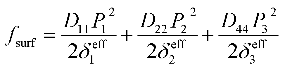 | (10) |
Phase-field simulation of domain switching of BTO thin film is performed by numerically solving the TDGL equations (eqn (4)) together with the mechanical and electrostatic equilibrium equations. For simplicity, a two-dimensional (2D) mesh along x and z direction is adopted. Thickness of the BTO film is taken to be 12 nm, and that of the substrate layer is taken to be 36 nm. The lateral size of the simulation cell is set to be 200 nm. A periodic boundary condition is applied along the x direction. The TDGL equations are solved by using an explicit Euler iterative scheme, whereas the mechanical and electrostatic equilibrium equations are solved by a finite element method (FEM). Values of the expansion coefficients of the Landau free energy, the electrostrictive coefficients and the elastic compliance coefficients are the same as those adopted in the thermodynamic calculation. Values of the gradient energy coefficients are taken to be: G11 = 5.1 × 10⁻¹⁰ m4 N C−2,  , and G12 = 0.41 The extrapolation lengths are δeff1 = δeff2 = δeff3 = 4.3 × 10⁻⁸ m.42
Results and discussion
Polarization state of BTO crystal at zero external electric field
We start our investigation on the temperature evolution of the polarization state of BTO crystal subjected to different values of shear stress σzx but at zero external electric field. For comparison, in Fig. 2a, the temperature evolution of the polarization state of BTO crystal in the absence of shear stress and external electric field is depicted. It can be seen that BTO undergoes a paraelectric–ferroelectric transition at about 395 K. The ferroelectric phase is c-phase at the temperature range of about [280 K, 395 K], O-phase at the temperature range of about [200 K, 280 K], and r1-phase at the temperature below 200 K. Note that, in the absence of shear stress and external electric field, polarization states with the polarization components in opposite signs are degenerate as a result of symmetry. Fig. 2b depicts the phase diagram of polarization state of BTO as a function of temperature and shear stress in the absence of external electric field. It can be seen that the application of shear stress lowers the degeneracy of the ferroelectric phases of BTO. In the negative stress regime, phases with the polarization components Px and Pz in opposite signs are stable. They are ac1-phase, ac2-phase and r2-phase. In contrast, in the positive stress regime, the stable phases are those with the polarization components Px and Pz in the same signs. They are ac3-phase, ac4-phase and r3-phase. The increase of shear stress magnitude |σzx| from zero to 4 GPa increases the paraelectric–ferroelectric transition temperature from about 395 K to above 520 K, meanwhile it decreases the ac2/r2 and the ac4/r3-phase transition temperatures from about 200 K to below 40 K. Note also that ac1 and ac3-phases are stable at relatively high temperature and small stress. With the increase of stress, the stable temperature window of the two phases decreases, forming two inverted triangular regions in the phase diagram.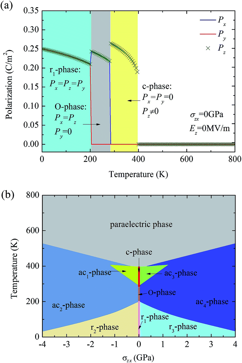 | ||
| Fig. 2 (a) Temperature evolution of polarization state of BTO in the absence of shear stress and external electric field. (b) Phase diagram of polarization state of BTO as a function of temperature and shear stress in the absence of external electric field. | ||
To see more clearly the change of polarization, in Fig. 3 we depict the temperature evolution of polarization state of BTO under different values of shear stress σzx and at zero external electric field, with Fig. 3a–d corresponding to σzx = −0.4 GPa, 0.4 GPa, −2 GPa, and 2 GPa, respectively. Paraelectric–ferroelectric phase transition occurs at a temperature of about 400 K for the cases of |σzx| = 0.4 GPa, whereas for |σzx| = 2 GPa the system exhibits paraelectric–ferroelectric phase transition at about 455 K. Moreover, the paraelectric–ferroelectric phase transition is first-order at |σzx| = 0.4 GPa and it turns to be second-order at |σzx| = 2 GPa. The ferroelectric phases are quite different due to the shear stress. Specifically, at σzx = −0.4 GPa, the system adopts ac1-phase at T = [325 K, 400 K], ac2-phase at T = [325 K, 280 K], and r2-phase at temperature below 170 K. At σzx = 0.4 GPa, the system adopts ac3-phase at T = [325 K, 400 K], ac4-phase at T = [325 K, 280 K], and r3-phase at temperature below 170 K. At σzx = −2 GPa, the system evolves into ac2-phase at about 455 K, then into r2-phase at about 95 K. At σzx = 2 GPa, the system evolves into ac4-phase at about 455 K, then into r2-phase at about 95 K. For negative stress σzx < 0, the two components Px and Pz are always in opposite signs, i.e., PxPz < 0, whereas for positive stress σzx > 0, they are always in positive signs, i.e., PxPz > 0. The change of direction of the two polarization components due to the change of sign of shear stress is clearly seen.
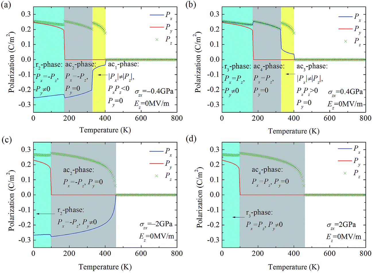 | ||
| Fig. 3 Temperature evolution of polarization state of BTO under different values of shear stress σzx and at zero external electric field. (a) σzx = −0.4 GPa, (b) σzx = 0.4 GPa, (c) σzx = −2 GPa and (d) σzx = 2 GPa. | ||
Polarization state of BTO crystal at nonzero external electric field
Note that while the above result indicates the feasibility of changing the relative sign of the two polarization components by shear stress, it is not deterministic which polarization component would change its sign when shear stress applies. This is due to the fact that, phases with Px > 0, Pz < 0 or Px < 0, Pz > 0 are possible at negative shear stress, meanwhile, phases with Px > 0, Pz > 0 or Px < 0, Pz < 0 are possible at positive shear stress. In practice, the direction of which polarization component will be switched depends on the relative stability of the two polarization components (see, Fig. 1b). Such relative stability can be modified by many factors, such as temperature, depolarization field, external electric field, and misfit strain. Take ferroelectric thin film as an example. The more stable polarization direction can be tuned from out-of-plane to in-plane when the misfit strain changes from compression to tension. Another possible effect that can lead to a deterministic switching is that the degeneracy of the polarization states with opposite polarization component is broken. For example, due to the application of an external field along positive z direction, states with Pz > 0 should be more stable than states with Pz < 0. As a result, a switching from states with Pz > 0 to states with Pz < 0 is not likely to trigger by the shear stress, hence Px rather than Pz would change sign. To see it more clearly, Fig. 4 depicts the stable polarization vector of BTO as a function of shear stress σzx and external electric field Ez at room temperature. Result shows that due to the external electric field, the direction of Pz component is controlled by the external field. Consequently, the direction of Px component depends on the sign of the shear stress. A deterministic switching of the Px component is thus achieved. Note that, besides the application of external field, the penalty of domain wall energy can also cause a broken degeneracy of the polarization states. A deterministic switching of the polarization can occur in a natural way without the need of an external field. This point will be clarified later by our phase-field simulation.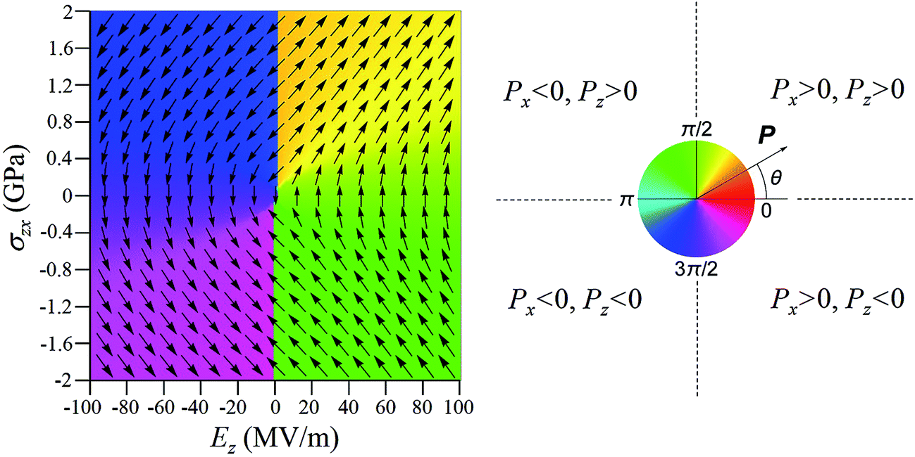 | ||
| Fig. 4 The stable polarization vector of BTO as a function of shear stress σzx and external electric field Ez at room temperature (left panel). Different colors correspond to different directions of the polarization vector as defined in the right panel. | ||
Moreover, Fig. 4 also indicates that when the shear stress σzx is fixed, the change of external field Ez can lead to switching of Pz component together with the switching of Px component. Therefore, shear stress can lead to a switching of in-plane polarization by an out-of-plane electric field. To see more clearly, in Fig. 5 we depict the polarization state of BTO as a function of external electric field under different values of shear stress σzx and at room temperature, with Fig. 5a–d corresponding to σzx = −0.4 GPa, 0.4 GPa, −2 GPa, and 2 GPa, respectively. It can be seen that while Pz component changes its sign with the inversion of the external field, Px also changes its sign with the inversion of the external field. Moreover, the signs of Px and Pz are either the same or opposite depending on the shear stress. Note also that while the magnitude of Pz increases as the external field increases, the magnitude of Px decreases with the external field. Such a change of the magnitude of Px can exhibit either a linear feature (see, Fig. 5c and d for |σzx| = 2 GPa) or a nonlinear feature (see, Fig. 5a and b for |σzx| = 0.4 GPa) depending on the magnitude of the shear stress.
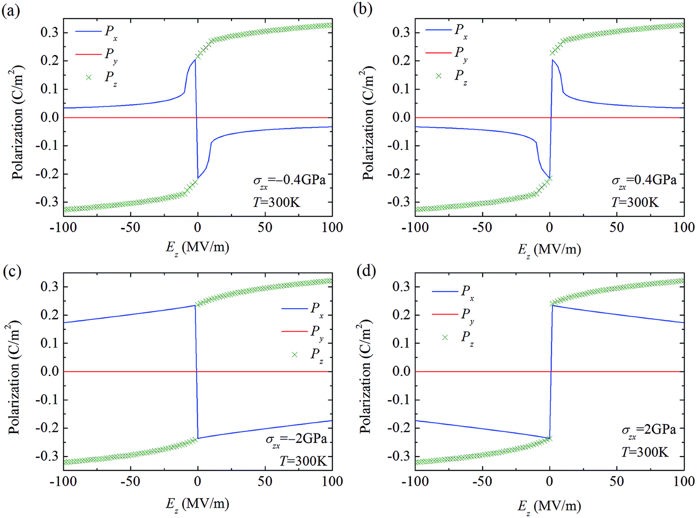 | ||
| Fig. 5 Polarization state of BTO at room temperature as a function of external electric field Ez under different values of shear stress σzx. (a) σzx = −0.4 GPa, (b) σzx = 0.4 GPa, (c) σzx = −2 GPa and (d) σzx = 2 GPa. | ||
Shear-stress-induced domain switching in ferroelectric thin film
The effects of shear stress/strain on polarization stability have been discussed by several works.25,30,43–45 Particularly, using a thermodynamic model, Zembilgotov et al.43 have calculated the phase diagrams of the stable polarization state in epitaxial films subjected to an in-plane misfit shear strain. Gruverman et al.44 observed that polarization switching could occur far beyond the tip contact area in polycrystalline films. Shear stress deformation of the grain underneath the tip was believed to cause this abnormal switching behavior. More recently, it has been shown that shear strain gradient can play a dominant role over compressive strain gradient in the flexoelectric domain switching process.25 First-principle calculation has been also applied to reveal the shear-strain gradient induced polarization reversal in BTO thin films.30 These works indicate that shear stress/strain (gradient) can be effective to control the polarization stability of ferroelectrics. Here we emphasize that polarization switching can be induced by shear stress, due to the trilinear coupling effect between shear stress and the two polarization components that lie in the shear strain plane. This shear stress effect has been overlooked in recent discussion on mechanical switching of ferroelectric polarization. Here we would like to first point out some implications of this effect on design of novel devices.First of all, this effect can be utilized to design generator or sensor devices based on ultrathin ferroelectric films. The merit of such devices lies in the fact that, in ultrathin ferroelectric films, depolarization field tends to force the polarization along the in-plane direction, which leads to a depression of piezoelectric response that utilizes the coupling of out-of-plane strain and polarization. In contrast, piezoelectric response based on the shear mode can enter into the role. This should has potential applications such as power generation or state detection of fluids where shear flow is important. Another potential application of the shear-stress-modified polarization switching effect is memory device. One possible working mode of the memory device is that exploits mechanical switching of the domain information without the need of external electric field. Domain switching can be induced in a thin film with orthorhombic or rhombohedral single-domain state, by exerting a local shear stress to the film. The local shear stress may be generated by the friction force via an AFM tip working at the sliding loading mode, or even under perpendicular loading mode. This is due to the fact that two shear stress regions with significant values can be induced inside a film when it is subjected to a compression tip force. Note that the contribution of shear stress to domain switching would be much less important for the switching of tetragonal single-domain state, as it is based on the coupling between two polarization components. Another possible working mode is that exploits the complicate domain switching behavior under the combining application of local shear stress and external electric field, which may be applied by a biased AFM tip working at the sliding mode. Note that for such a working mode, head-to-head or tail-to-tail charged domain walls can be generated in a deterministic way according to the result shown in Fig. 4. Such charged domain walls can be stabilized in samples with enough free charge carriers. This should be very useful for the design of domain-wall-based memory devices.
To verify the feasibility of domain switching via shear stress, we further perform phase-field simulation on a 12 nm-thick BTO thin film under the contact of an AFM tip (with a radius of 50 nm) at the film surface. The AFM tip is subjected to a compression force Fp along the film thickness direction (i.e., negative z direction), which imposes a nonuniform surface traction τz within the contact region. Moreover, the tip has a trend of relative motion along the film surface (i.e., positive or negative x direction). This leads to a lateral surface traction τx due to the static friction. Assuming that the static friction coefficient is μ, we have τx = μτz, and the static friction force Ff = μFp. Fig. 6 depicts the distributions of stress components σzz and σzx in the film under a tip force Fp = 1.8 μN with a trend of relative motion along the negative x direction. It can be seen that the tip force induces a compressive stress state σzz along the film direction right below the tip (Fig. 6a). Moreover, it also causes two shear stress regions with σzx taking opposite signs in the film at the two sides of the tip (Fig. 6b). Due to the trend of relative motion along the negative x direction, the magnitude of shear stress at the left side (in front of the tip) is much larger than that at the right side (behind the tip).
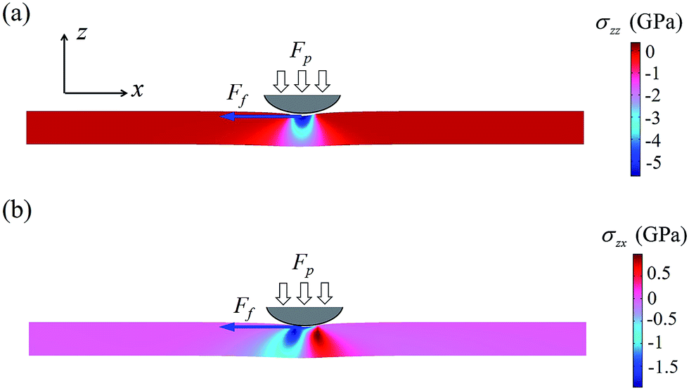 | ||
| Fig. 6 Distributions of stress components (a) σzz and (b) σzx in a 12 nm-thick BTO film under a tip force Fp = 1.8 μN. The tip has a trend of relative motion along the negative x direction. | ||
In the following, we explore if domain switching can occur at the enhanced shear stress region. The electric boundary condition at the top and bottom surfaces of the film is set to be short-circuited. The simulation temperature is set to be 100 K and the misfit strain is −0.002 so that the film can be stabilized in a rhombohedral phase. The thin film is initially set into a single-domain state with Px > 0 and Pz > 0. The evolution of this single-domain state in response to the tip force shown above is simulated and the result is shown in Fig. 7a. In response to the local shear stress σzx < 0, the polarization field nearby the stress-applied region is expected to be switched into Px < 0 and Pz > 0, or Px > 0 and Pz < 0. However, in fact, the polarization field is definitely switched into Px > 0 and Pz < 0; otherwise, head-to-head and tail-to-tail charged domain walls will appear, which violates the energy minimization principle. An up-to-down domain switching thus can occur at the shear stress region with σzx < 0. This is exactly the case we found in Fig. 7a. One can see that, as the tip force is applied, the polarization field below the tip becomes mainly along the in-plane direction due to the large compressive stress. Moreover, the polarization field near the left side of the tip (i.e., at the enhanced shear stress region with σzx < 0) is switched to negative z direction. After the tip force is switched off, a switched domain with Px > 0 and Pz < 0 is formed slightly ahead of the tip. Similarly, we also simulate the case where the thin film is initially set into a single-domain state with Px > 0 and Pz < 0, and the trend of relative motion is changed to be along the positive x direction. As shown in Fig. 7b, a down-to-up domain switching has been triggered by a local tip force. For this case, the switched domain with Px > 0 and Pz > 0 is formed, and its location is also slightly ahead of the tip. Note that our result shows that shear stress can lead to both up-to-down and down-to-up domain switching, which is determined by the sliding direction and the polarization direction of domain. This is different from flexoelectric domain switching in tip-film architecture, where the directions of strain gradients and flexoelectric field are fixed, thus one can only expect either up-to-down or down-to-up switching. Note also that, for a film under sliding load, previous work showed that the domain switching due to flexoelectric field includes a region behind the sliding tip, which is determined by the distribution of the shear strain gradient.25 This is in contrast to our case, where the switched domain is slightly ahead of the tip, as determined by the distribution of the shear stress and the direction of the polarization field (Fig. 6b). In practice, the feasibility of bi-directional switching and the location of switching domain could be evidences of mechanical switching beyond flexoelectricity.
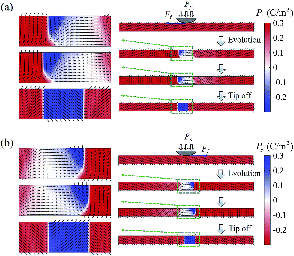 | ||
| Fig. 7 Phase-field simulation result of domain switching in a 12 nm-thick BTO thin film subjected to a tip force Fp = 1.8 μN. (a) Up-to-down domain switching for the tip with a trend of relative motion along the negative x direction (b) down-to-up domain switching for the tip with a trend of relative motion along the positive x direction. | ||
As pointed out previously, it is also possible to generate charged domain walls in thin film under the combining effect of shear stress and external electric field. To see this, we perform another simulation, with all of the setting similar to the case shown in Fig. 7a, except that now an external electric field Ez = 3 × 10⁸ V m−1 is also applied to the thin film (at the middle region of the film with a width 80 nm), mimicking a biased tip working at the sliding mode. The simulation result is shown in Fig. 8. It can be seen that the polarization field nearby the stress and field applied region is switched into Px < 0 and Pz > 0, with the appearance of tail-to-tail and head-to-head alike domain walls between the switched domain and the unswitched domains, in contrast to the case shown in Fig. 7a where charge neutral domain walls are formed instead. The difference is due to the fact that, the direction of polarization component Pz is fixed here due to the external electric field, therefore the polarization component Px has to be switched by the shear stress according to the trilinear coupling. It should be pointed out that the shear-stress-induced charged domain walls we found here is not strictly tail-to-tail and head-to-head to avoid the depolarization energy (as no free charge carriers is assumed), and the domain walls would not maintain stable after tip force and field is switched off. Nevertheless, such charged domain walls in practice could be stabilized by free charges and mobile charge defects such as oxygen vacancies in the ferroelectric film, similar to those reported in previous experimental works.46–50 Our result thus indicates a novel method to write charged domain walls.
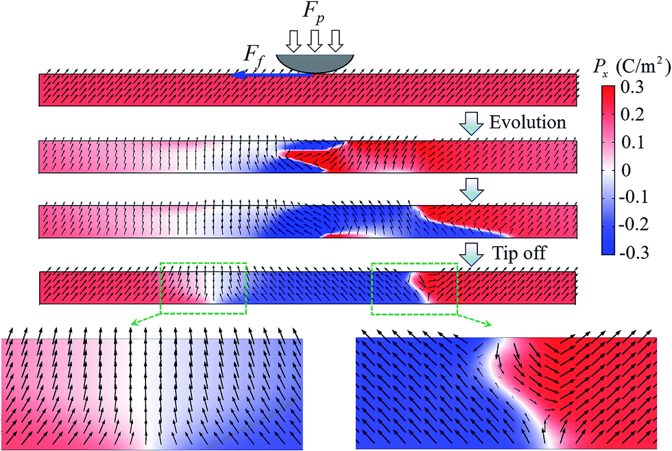 | ||
| Fig. 8 Phase-field simulation result of domain switching in a 12 nm-thick BTO thin film with the formation of charged domain walls under the combining application of a tip force Fp = 1.8 μN and an external electric field Ez = −3 × 10⁸ V m−1. The tip has a trend of relative motion along the negative x direction. | ||
Shear-stress-induced vortex switching in ferroelectric nanoring
Finally, it is noteworthy that the trilinear coupling between the shear stress and the polarization components also indicates a potential strategy of switching the chirality of ferroelectric vortices. Although it is very attractive to utilize the chirality of ferroelectric vortices to develop high-density information storage, switching of the vortex chirality is challenged so far. This is due to the lack of a bilinear coupling between the electric field without curl and the toroidization. Here we show that shear stress might help solve the problem. The basic idea is schematically illustrated in Fig. 9, where switching of the vortex formed in a ferroelectric nanoring with a radius R is taken as an example. The system is placed in a cylindrical coordinate system (ρ, φ, z). For simplicity, we assume that the nanoring has a uniform polarization Pφ along the angular direction, and is subjected to a shear stress σφz, which can be exerted by a torque to the nanoring. The toroidization of the nanoring is given by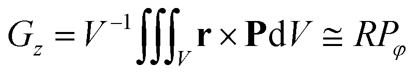 . Then we apply an external field along the z direction so that the polarization component Pz is induced. The coupling energy density between the shear stress and the two polarization components is fc = −QσφzPφPz, with Q being the electrostrictive constant. After integrating fc over the volume of the nanoring, one can obtain the coupling energy
  , with A being a constant related to the geometry parameters of the ring. Therefore, the toroidization Gz, the polarization Pz and the shear stress σφz are coupled in a trilinear form. For a fixed shear stress σφz, a change sign of Pz, which is controlled by the external electric field, can lead to a change sign of the toroidization Gz. Moreover, if the external electric field is fixed so that Pz is fixed in sign, a change sign of shear stress σφz can also lead to a reversal of the toroidization Gz. Note that a polar-toroidal state (Gz ≠ 0, Pz ≠ 0) is necessary for the appearance of the trilinear coupling. Usually one can apply an external field to induce such a polar-toroidal state. In some systems, polar-toroidal state can be spontaneously formed, e.g., in ferroelectric/paraelectric nanowires.51 In a future simulation work, we would like to show that these systems are promising to realize electric and mechanical switching of the vortex chirality. The feasibility of a simple switching strategy of the chirality of ferroelectric vortices should be very useful for vortex memory devices.
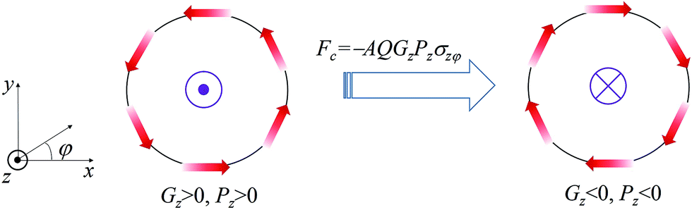 | ||
| Fig. 9 Schematic of vortex switching in a ferroelectric nanoring based on the trilinear coupling between toroidization Gz, polarization component Pz, and shear stress σzφ. | ||
Conclusions
Thermodynamic calculation and phase-field simulation have been performed to reveal the effect of shear stress on the polarization switching behavior in ferroelectric with orthorhombic or rhombohedral phase. Using BTO as an example, we show that switching of polarization can be achieved by shear stress via a simple mechanism. In this mechanism, the trilinear coupling between shear stress and the two polarization components that lie in the strain plane is exploited. Phase diagrams of polarization state as a function of shear stress, temperature and electric field are calculated. The shear-stress-induced domain switching in ferroelectric thin film is verified by phase-field simulation. In addition to the normal domain switching where neutral domain walls are involved, abnormal domain switching with the formation of charged domain walls can be achieved via the combining application of shear stress and electric field. The role of shear stress in the feasibility of chirality switching of ferroelectric vortices is also discussed. Our work sheds light on the potential use of shear stress or strain in domain engineering of ferroelectrics.Conflicts of interest
There are no conflicts to declare.Acknowledgements
This work was supported by the National Key Basic Research Program of China (No. 2015CB351905), NSFC (No. 11474363, 51172291, 11602310). Yue Zheng also thanks support from Special Program for Applied Research on Super Computation of the NSFC-Guangdong Joint Fund (the second phase), Fok Ying Tung Foundation, Guangdong Natural Science Funds for Distinguished Young Scholar and China Scholarship Council.References
- J. F. Scott, Ferroelectric Memories, Springer-Verlag, Berlin, 2000 Search PubMed.
- D. Damjanovic, P. Muralt and N. Setter, IEEE Sens. J., 2001, 1, 191 CrossRef CAS.
- P. Muralt, J. Micromech. Microeng., 2000, 10, 136 CrossRef CAS.
- J. D. Childress, J. Appl. Phys., 1962, 33, 179 CrossRef.
- K. T. Butler, J. M. Frost and A. Walsh, Energy Environ. Sci., 2015, 8, 38 Search PubMed.
- C. W. Lo, C. Li and H. Jiang, AIP Adv., 2011, 1, 687 Search PubMed.
- K. Kondo, Y. Sato, K. Miyasato, H. Takezoe, A. Fukuda, E. Kuze, K. Flatischler and K. Skarp, Jpn. J. Appl. Phys., 1983, 22, 1 CrossRef.
- M. J. Lancaster, J. Powell and A. Porch, Supercond. Sci. Technol., 1998, 11, 1323 CrossRef CAS.
- A. S. Mischenko, Q. Zhang, J. F. Scott, R. W. Whatmore and N. D. Mathur, Science, 2006, 311, 1270 CrossRef CAS PubMed.
- T. Choi, S. Lee, Y. J. Choi, V. Kiryukhin and S. W. Cheong, Science, 2009, 324, 63 CrossRef CAS PubMed.
- Z. Kutnjak, J. Petzelt and R. Blinc, Nature, 2006, 441, 956 CrossRef CAS PubMed.
- R. Soni, A. Petraru, P. Meuffels, O. Vavra, M. Ziegler, S. K. Kim, D. S. Jeong, N. A. Pertsev and H. Kohlstedt, Nat. Commun., 2014, 5, 5414 CrossRef PubMed.
- A. V. Ievlev, A. N. Morozovska, E. A. Eliseev, V. Y. Shur and S. V. Kalinin, Nat. Commun., 2014, 5, 4545 CAS.
- J. J. Yang, M. D. Pickett, X. Li, D. A. Ohlberg, D. R. Stewart and R. S. Williams, Nat. Nanotechnol., 2008, 3, 429 CrossRef CAS PubMed.
- M. D. Pickett, D. B. Strukov, J. L. Borghetti, J. J. Yang, G. S. Snider, D. R. Stewart and R. S. Williamsb, J. Appl. Phys., 2009, 106, 074508 CrossRef.
- H. Lu, C. W. Bark, d. l. O. D. Esque, J. Alcala, C. B. Eom, G. Catalan and A. Gruverman, Science, 2012, 336, 59 CrossRef CAS PubMed.
- X. Chen, X. Tang, X. Z. Chen, Y. L. Chen, X. Guo, H. X. Ge and Q. D. Shen, Appl. Phys. Lett., 2015, 106, 1400 Search PubMed.
- R. G. Cai, B. Nysten, Z. J. Hu and A. M. Jonas, Appl. Phys. Lett., 2017, 110, 202901 CrossRef.
- L. Chen, Z. Cheng, W. Xu, X. Meng, G. Yuan, J. Liu and Z. Liu, Sci. Rep., 2016, 6, 19092 CrossRef CAS PubMed.
- T. Jia, H. Kimura, Z. Cheng and H. Zhao, Sci. Rep., 2016, 6, 31867 CrossRef CAS PubMed.
- Y. J. Li, J. J. Wang, J. C. Ye, X. X. Ke, G. Y. Gou, Y. Wei, F. Xue, J. Wang, C. S. Wang, R. C. Peng, X. L. Deng, Y. Yang, X. B. Ren, L. Q. Chen, C. W. Nan and J. X. Zhang, Adv. Funct. Mater., 2015, 25, 3405 CrossRef CAS.
- A. Gómez, J. M. Vila-Fungueiriño, R. Moalla, G. Saint-Girons, J. Gázquez, M. Varela, R. Bachelet, M. Gich, F. Rivadulla and A. Carretero-Genevrier, Small, 2017, 13, 1701614 CrossRef PubMed.
- Z. Wen, X. Qiu, C. Li, C. Zheng, X. Ge, A. Li and D. Wu, Appl. Phys. Lett., 2014, 104, 042907 CrossRef.
- E. J. Guo, R. Roth, S. Das and K. Dörr, Appl. Phys. Lett., 2014, 105, 012903 CrossRef.
- J. Očenášek, H. Lu, C. W. Bark, C. B. Eom, J. Alcalá, G. Catalan and A. Gruverman, Phys. Rev. B: Condens. Matter Mater. Phys., 2015, 92, 035417 CrossRef.
- H. Lu, S. Liu, Z. Ye, S. Yasui, H. Funakubo, A. M. Rappe and A. Gruverman, Appl. Phys. Lett., 2017, 110, 222903 CrossRef.
- W. J. Chen, Y. Zheng, X. Feng and B. Wang, J. Mech. Phys. Solids, 2015, 79, 108 CrossRef CAS.
- Y. Gu, Z. Hong, J. Britson and L. Q. Chen, Appl. Phys. Lett., 2015, 106, 022904 CrossRef.
- L. Jiang, X. Xu, Y. Zhou, Y. Zhang and Q. Yang, RSC Adv., 2016, 6, 80946 RSC.
- G. Li, X. Huang, J. Hu and W. Zhang, Phys. Rev. B, 2017, 95, 144111 CrossRef.
- J. Narvaez, F. Vasquez-Sancho and G. Catalan, Nature, 2016, 538, 219 CrossRef CAS PubMed.
- W. J. Chen, Y. Zheng, X. Luo, B. Wang and C. H. Woo, J. Appl. Phys., 2013, 114, 064105 CrossRef.
- W. J. Chen, J. Y. Liua, L. L. Ma, L. J. Liu, G. L. Jiang and Y. Zheng, J. Mech. Phys. Solids, 2018, 111, 43 CrossRef CAS.
- T. Sluka, A. K. Tagantsev, P. Bednyakov and N. Setter, Nat. Commun., 2013, 4, 1808 CrossRef PubMed.
- A. V. Ievlev, S. Jesse, A. N. Morozovska, E. Strelcov, E. A. Eliseev, Y. V. Pershin, A. Kumar, V. Y. Shur and S. V. Kalinin, Nat. Phys., 2014, 10, 59 CrossRef CAS.
- Y. C. Shu and K. Bhattacharya, Philos. Mag. B, 2001, 81, 2021 CrossRef CAS.
- Y. L. Li, L. E. Cross and L. Q. Chen, J. Appl. Phys., 2005, 98, 064101 CrossRef.
- N. A. Pertsev, A. G. Zembilgotov and A. K. Tagantsev, Phys. Rev. Lett., 1998, 80, 1988 CrossRef CAS.
- Y. Zheng and C. H. Woo, Appl. Phys. A: Mater. Sci. Process., 2009, 97, 617 CrossRef CAS.
- C. H. Woo and Y. Zheng, Appl. Phys. A: Mater. Sci. Process., 2008, 91, 59 CrossRef CAS.
- J. Hlinka and P. Márton, Phys. Rev. B: Condens. Matter Mater. Phys., 2006, 74, 104104 CrossRef.
- K. Ishikawa and T. Uemori, Phys. Rev. B: Condens. Matter Mater. Phys., 1999, 60, 11841 CrossRef CAS.
- A. G. Zembilgotov, U. Böttger and R. Waser, J. Appl. Phys., 2008, 104, 054118 CrossRef.
- A. Gruverman, A. Kholkin, A. Kingon and H. Tokumoto, Appl. Phys. Lett., 2001, 78, 2751 CrossRef CAS.
- Z. Wu and H. Krakauer, Phys. Rev. B: Condens. Matter Mater. Phys., 2013, 68, 014112 CrossRef.
- P. Gao, J. Britson, J. R. Jokisaari, C. T. Nelson, S. H. Baek, Y. Wang, C. B. Eom, L. Q. Chen and X. Q. Pan, Nat. Commun., 2013, 4, 2791 Search PubMed.
- Y. L. Tang, Y. L. Zhu, Y. J. Wang, W. Y. Wang, Y. B. Xu, W. J. Ren, Z. D. Zhang and X. L. Ma, Sci. Rep., 2014, 4, 04115 CrossRef CAS PubMed.
- A. Crassous, T. Sluka, A. Tagantsev and N. Setter, Nat. Nanotechnol., 2015, 10, 614 CrossRef CAS PubMed.
- T. Sluka, A. K. Tagantsev, P. Bednyakov and N. Setter, Nat. Commun., 2013, 4, 1808 CrossRef PubMed.
- D. Meier, J. Seidel, A. Cano, K. Delaney, Y. Kumagai, M. Mostovoy, N. A. Spaldin, R. Ramesh and M. Fiebig, Nat. Mater., 2012, 11, 284 CrossRef CAS PubMed.
- W. J. Chen, Y. Zheng and B. Wang, Sci. Rep., 2015, 5, 11165 CrossRef CAS PubMed.
| This journal is © The Royal Society of Chemistry 2018 |