
 Open Access Article
 This Open Access Article is licensed under a Creative Commons Attribution-Non Commercial 3.0 Unported Licence
Preparation and in-system study of SnCl2 precursor layers: towards vacuum-based synthesis of Pb-free perovskites†
R. Félix‡
 *a,
N. Llobera-Vila‡a,
C. Hartmanna,
C. Klimma,
M. Hartigab,
R. G. Wilksac and
M. Bärac
*a,
N. Llobera-Vila‡a,
C. Hartmanna,
C. Klimma,
M. Hartigab,
R. G. Wilksac and
M. Bärac
aRenewable Energy, Helmholtz-Zentrum Berlin für Materialien und Energie GmbH, Hahn-Meitner-Platz 1, D-14109 Berlin, Germany. E-mail: roberto.felix_duarte@helmholtz-berlin.de
bTechnologie für Dünnschicht-Bauelemente, Technische Universität Berlin - Fak. IV, HFT 5-2, Einsteinufer 25, D-10587 Berlin, Germany
cEnergy Materials In-Situ Laboratory Berlin (EMIL), Helmholtz-Zentrum Berlin für Materialien und Energie GmbH, Albert-Einstein-Straße 15, D-12489 Berlin, Germany
First published on 3rd January 2018
Abstract
The chemical structure and topography evolution of vapor-deposited SnCl2 thin-films on Mo-coated glass substrates was studied via a combination of electron spectroscopies and scanning electron microscopy. For this purpose, a thickness series of SnCl2 thin-films was prepared using different evaporation times, revealing significant changes in the chemical environment of Sn and Cl along the layer profile and layer topography. The presence of O in the Mo-coated substrates can lead to oxidation in the SnCl2 film layers. The findings in this work show the effect that substrate conditions can exert on the chemical (and electronic) properties of the deposited material layers and that need to be taken into account for device optimization.
Introduction
In the last decade, hybrid organic–inorganic perovskites (HOIP) – particularly those using APbX3 [A = CH3NH3+, HC(NH2)2+, Cs+ and X = I−, Cl−, Br−] as the absorber layer – have emerged as a novel class of semiconductors with potential for high-performance photovoltaic (PV) applications due to their strong light-harvesting properties.1 An attractive advantage of HOIP compounds in PV technology is that, compared to most other absorber materials, their synthesis process is relatively simple: perovskite conversion typically entails the mixture and crystallization of the organic and inorganic precursors either by a one-step (i.e., a mixing of two precursors)2 or a two-step (i.e., the inorganic precursor is initially deposited onto a substrate, followed by the deposition of the organic precursor)2–4 method. The most widely studied HOIP compounds are based on PbX2 (X = Br, I, Cl) inorganic precursors and methylammonium iodide (MAI) as the organic precursor.5,6 Power conversion efficiencies (η) of solar cells based on this class of absorber materials have already reached record values of 22.1% on a laboratory-scale.1,7 However, high performance solar devices have also been synthesized using a wide range of other organic–inorganic precursors.8Due to strict legal regulations concerning the handling of heavy metal Pb, its presence is regarded as a (potential) drawback for the commercial large-scale implementation of perovskites in PV technology, and thus substituting Pb by less-toxic Sn§ in perovskite solar cell absorbers is suggested as a solution. Currently, a wider use of Sn-based perovskite absorbers in solar cell has been in general hampered by the ease of Sn to oxidize (i.e., from Sn2+ to Sn4+), resulting in material properties (e.g., poor conductivity, limited stability, etc.) adversely affecting solar cell performance.10–14 In principle, a strategy to minimize this oxidation could entail a two-step perovskite conversion method, in which the Sn-containing precursor (e.g., SnCl2) is deposited under conditions that prevent oxidation [e.g., in ultra-high vacuum (UHV)].12,15
In this work, the first experimental results towards synthesizing Pb-free perovskite thin-films at the Energy Materials In Situ Laboratory Berlin (EMIL)16 are presented. It consists of a detailed X-ray photoelectron and Auger electron spectroscopy study of SnCl2 precursor layers of different thicknesses UHV-deposited on Mo-coated glass substrates, which reveals significant changes in the chemical environment of Sn and Cl along the layer profile. These findings highlight that not only the deposition environment can impact the deposited material but that substrate conditions also play a crucial role.
Experimental
Materials and methods
Thin films of SnCl2 were deposited on 25 × 25 mm2 SGG DIAMANT® substrates coated with 200 nm films of sputtered-Mo. Prior to the SnCl2 deposition treatments, the Mo-coated SGG substrates were cleaned by immersing them in solutions of 30% aqueous ammonium hydroxide (NH4OH). To further remove surface adsorbates, substrates were submitted to 20 min cycles of Ar+-ion treatments (ion energies up to 3 keV) using a Nonsequitur Technologies 1402 ion gun17 attached to the UHV preparation chamber (base pressure < 5.0 × 10⁻⁹ mbar).SnCl2 powder 98% (Sigma-Aldrich) was used to deposit thin films by using a conventional 4-pocket evaporator (Dr Eberl MBE Komponenten Quad Cluster Source)18 attached to the UHV deposition chamber (base pressure < 1.0 × 10⁻⁸ mbar) directly connected to the preparation chamber where the Ar+ ion treatments were carried out. Eight different SnCl2 thin-film depositions were carried out by varying the evaporation periods (i.e., between 25 s and 1600 s), using a constant crucible temperature (i.e., 112 °C). In the following, each sample will be referred to by the SnCl2 evaporation time used to prepare it.
X-ray photoelectron spectroscopy (XPS) and X-ray-excited Auger electron spectroscopy (XAES)
The surface chemical structure of the samples was characterized via X-ray photoelectron spectroscopy (XPS) and X-ray-excited Auger electron spectroscopy (XAES), using a Scienta EW4000 electron analyser19 and non-monochromatized Mg Kα excitation from a PREVAC RS40B1 twin anode X-ray source.20 Curve fit analysis of measured detail XPS spectra were simultaneously conducted with the Fityk software.21 Voigt profile functions, along with linear backgrounds, were used for these fits. Spin–orbit doublets were fitted with two Voigt functions with intensity ratios set to obey the 2j + 1 multiplicity rule. The energy scale for these measurements was calibrated in accordance to ref. 22.Scanning electron microscopy (SEM)
The thickness and morphology of the deposited SnCl2 films were evaluated through scanning electron microscopy (SEM) measurements using a SEM Hitachi S 4100.23 [Due to sample surface charging effects observed for the “1600 s” sample, only its SEM – and not the XPS/XAES – characterization results are discussed in this work (i.e., the encountered surface charging distorts the XPS and XAES results yet still allows for satisfactory SEM images).]Results and discussion
Fig. 1 shows the XPS survey spectra of a (cleaned) Mo-coated substrate and the produced SnCl2 thin-film sample series. The survey spectrum of the substrate sample consists of signature Mo-derived lines, as well as, low-intensity O lines ascribed to remaining adsorbates. Sn- and Cl-related spectral lines are detected for all SnCl2 evaporated samples. As expected, an increase in intensity of Sn- and Cl-related spectral lines is observed with SnCl2 evaporation (i.e., in samples with treatments ranging from 25–400 s), along with a corresponding decrease in Mo-related spectral lines. The survey spectra of samples treated with evaporations periods of at least 600 s no longer show Mo-related spectral lines, indicating complete coverage of the Mo substrate by SnCl2 films with a minimal thickness greater than the XPS information depth [i.e., the inelastic mean free path (IMFP) – describing the exponential decay of electrons travelling through matter – of Cl 2p3/2, Mo 3d5/2 and Sn 3d5/2 electrons with kinetic energies (KE) of ∼1055 eV, 1026 eV, and 769 eV is approximately 2 nm in SnCl2.24,25 The XPS information depth (ID) is taken as 3× IMFP.]. | ||
| Fig. 1 Mg Kα-excited XPS survey spectra of the SnCl2 thin-film thickness series on Mo, along with identification of core level and Auger lines. Vertical offsets are added for clarity. | ||
Changes in layer thickness and topography as a function of SnCl2 evaporation time were studied through SEM. Fig. 2(a)–(h) presents 30°-tilted cross section SEM images of the investigated sample series, indicating a change of morphology of the deposited SnCl2. [The ESI† presents non-tilted cross section SEM images of the sample series (cf., Fig. S1† for more details).] While the SEM image of the “25 s” sample appears homogeneous, starting from the “50 s” sample the formation of islands can be observed. Samples for which SnCl2 layers have been deposited between 100–400 s (and especially for the “200 s” sample) show that the deposited SnCl2 material grows vertically, forming islands with peak heights of up to 150 ± 25 nm (cf. ESI; Fig. S1† for more details), but leaving a large substrate/seeding layer area exposed. With longer evaporation treatments (e.g., “400 s” and “600 s” samples), the islands grow laterally and further cover a greater substrate/seeding layer area, while maintaining their peak heights unchanged. Once the islands coalesce (e.g., “800 s” and “1600 s” samples), the SnCl2 film thickness resumes its vertical growth; the thickness of the SnCl2 film for the “1600 s” sample is (715 ± 25) nm.
 | ||
Fig. 2 30°-Tilted cross section scanning electron microscope (SEM) images of SnCl2/Mo samples with the following evaporation times: (a) 25 s, (b) 50 s, (c) 100 s, (d) 200 s, (e) 400 s, (f) 600 s, (g) 800 s, and (h) 1600 s. SEM images (a)–(g) were taken with a 30![[thin space (1/6-em)]](https://www.rsc.org/images/entities/char_2009.gif) 000× magnification, whereas (h) shows a 10000× magnification. 000× magnification, whereas (h) shows a 10000× magnification. | ||
The effect of the changes in morphology of the deposited SnCl2 is clearly observed in the signal evolution of detail XPS spectra of the Mo 3d (substrate) and Sn 3d and Cl 2p (cover layer) lines of the sample series, shown in Fig. 3 as a function of evaporation time. The values in the plots are shown normalized to highest (obtained) intensity value in the series [i.e., the Mo 3d value of the bare (cleaned) Mo-coated substrate and the Sn 3d and Cl 2p values of the “800 s” sample]. Included in the figure, denoted by solid lines, are intensification/attenuation signal trends expected for a layer-by-layer (i.e., Frank-van der Merwe) growth mode as a function of the SnCl2 thickness (in multiples of IMFP values).26,27 Note that this model assumes complete and homogeneous coverage of the substrate by the cover layer; in a nonuniform system, it describes the “effective” thickness of the layer. For short evaporation times (i.e., 25 s and 50 s), an agreement between the observed relative intensity Cl 2p/Mo 3d values and the expected signal trends is found. (Although the relative intensity values of the Sn 3d and Cl 2p lines follow a similar trend as a function of evaporation time, significant differences are found for the values of these two core levels for samples with evaporation treatments of up to 200 s. The apparent deposition of Cl-rich layers may arise due to Cl-termination of the SnCl2 or diffusion of Sn into the Mo.)28,29 In fact, the relative intensity values of the Cl 2p and Mo 3d lines of the “50 s” sample (i.e., 0.40 ± 0.05 and 0.62 ± 0.05) nearly match the intensification/attenuation effects of a SnCl2 deposition thickness equivalent to one IMFP value (i.e., ca. 2 nm), indicated by the vertical dashed line in Fig. 3. This finding suggests that at least a seeding layer that homogeneously covers the substrate is formed during these evaporation times, in agreement with the SEM images of the “25 s” and “50 s” samples. Deviations from these trends are found for the values of samples with evaporation treatments between 100–400 s, with the XPS Cl 2p/Mo 3d relative intensity values of the “50 s”, “100 s” and “200 s” samples remaining statistically constant due to the large substrate/seeding layer area exposed in them (as pointed out in the SEM discussion above). With longer evaporation treatments, the XPS Sn 3d (Mo 3d) relative intensity of samples starts to increase (attenuate) in a more-linear-than-exponential way, in agreement with the observed island lateral (rather than vertical) growth for these evaporation times. The XPS and SEM results indicate that the deposition of SnCl2 layers on Mo-coated substrates follows a Stranski–Krastanov (SK) growth mode:26 the formation of a seeding layer (i.e., 25 s and 50 s evaporation treatments) with subsequent island formation (i.e., 100–600 s evaporation treatments), ultimately fusing into a film (i.e., 800 s and 1600 s evaporation treatments).
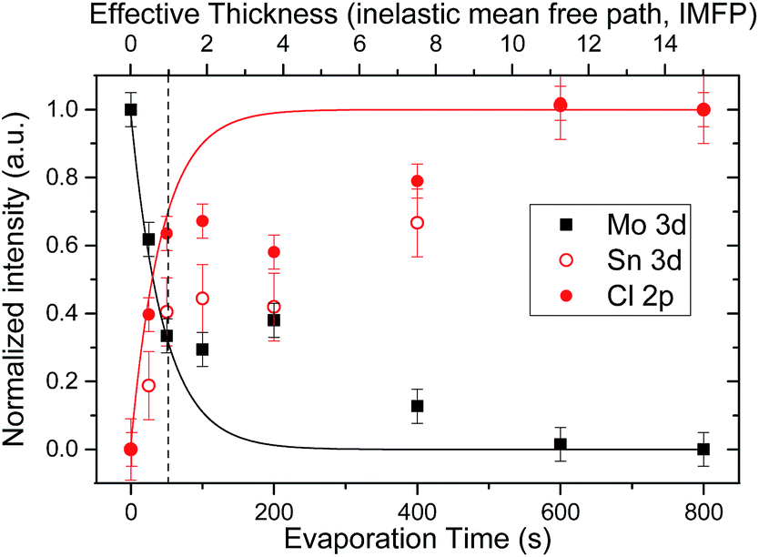 | ||
| Fig. 3 Relative intensities of Sn 3d, Cl 2p, and Mo 3d lines as a function of SnCl2 evaporation time in the sample series. The solid lines show intensity evolutions expected of a homogeneous layer-by-layer deposition of SnCl2 as a function of its effective thickness (in multiples of IMFP values). The vertical dashed line indicates a SnCl2 effective thickness equal to one IMFP value (i.e., ca. 2 nm).¶ | ||
To gain insight into the chemical structure of the deposited SnCl2 films, the XPS Sn 3d and Cl 2p energy regions of the sample series were investigated. In Fig. 4, the detail XPS spectra of the (a) Sn 3d and (b) Cl 2p energy regions of the “25 s” and “800 s” samples are shown, normalized to maximum intensity. To better illustrate changes in spectral width, the binding energy (BE) scales of the spectra were shifted so that the maxima overlap to the one of the “800 s” spectra. The peak widths of the spectra of the “25 s” sample are significantly larger than for the spectra of the “800 s” sample, indicating differences in chemical environment at the start and end of the SnCl2 deposition of the investigated sample series. For the “800 s” sample additional spectral intensity between 494 and 493 eV can be observed for the Sn 3d line, which will be discussed below. Fig. 4(c) shows the evolution of the full width at half maximum (FWHM) values of the Sn 3d and Cl 2p lines as a function of evaporation time. A reduction in FHWM values, for both spectral lines, following the same trend – but more pronounced for the Sn 3d – with evaporation treatment can be seen. [A similar effect is observed for the XPS spectra of the Mo 3d energy region of samples produced by evaporation times in the 25–400 s range (cf. ESI; Fig. S2† for more details).] The broader spectral peak shapes detected for samples with shorter evaporation treatments suggest a greater degree of chemical speciation for Sn and Cl in the interfacial region (i.e., the seeding layer).
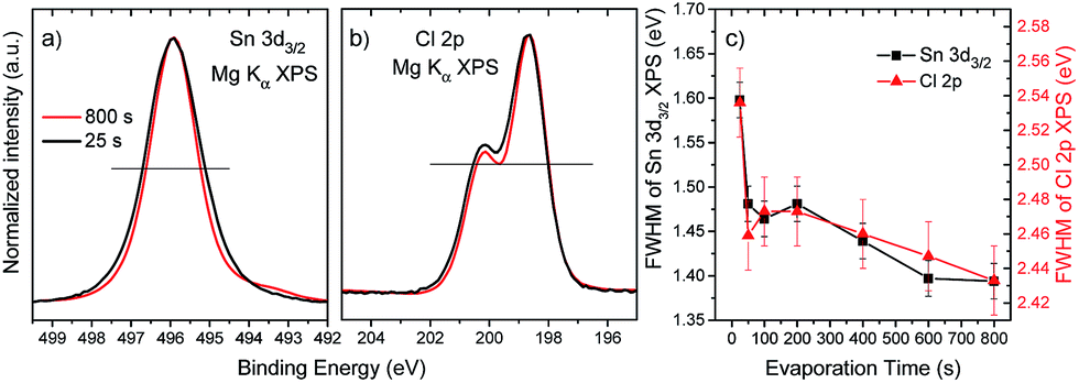 | ||
| Fig. 4 Detail XPS spectra of the (a) Sn 3d3/2 and (b) Cl 2p energy regions of the “25 s” and “800 s” samples. Spectra are normalized to maximum intensity for shape comparison. The binding energy scale of the “25 s” spectrum was shifted to overlap the spectra maxima. The (outer) intersections of the horizontal black lines with the spectra were used for the full width at half maximum (FWHM) evaluation. (c) FWHM values of the Sn 3d and Cl 2p lines as a function of SnCl2 evaporation time in the sample series. | ||
The results of the curve fit analysis of the XPS Sn 3d3/2 lines, three of which (i.e., for the “25 s”, “200 s” and “800 s” spectra) are shown in Fig. 5(a), reveal the presence of three peaks originating from different Sn chemical species. [Each of these selected treatment times represent different morphological stages of the SK growth mode of the SnCl2 films: seeding layer (i.e., “25 s”), layer-plus-island (i.e., “200 s”), and coalesced film (i.e., “800 s”).] The Sn 3d3/2 line is chosen for this analysis to avoid overlap with spectral intensity excited by X-ray satellite energies derived from the non-monochromatic X-ray source. The ESI† shows the complete set of the curve fit analysis of the Sn 3d3/2 spectra (cf. Fig. S3† for more details). The main peak contribution (i.e., SnI) is located at a BE of (495.9 ± 0.1) eV, a value close to BE values reported for Sn-halide bonds,30 and is ascribed to the evaporated material (i.e., SnCl2). The second peak contribution (i.e., SnII) of much lower intensity is located at a BE of (495.2 ± 0.1) eV and corresponds in literature to compounds with Sn–O bonds.30–36 The oxygen source appears to be the O remaining in the surface of the Mo-coated substrates (in the form of MoOx); the change of the XPS Mo 3d spectra of samples with short and intermediate evaporation times indicates a leaching of O from Mo (cf. ESI; Fig. S2† for more details and supporting thermodynamic considerations). The leaching of the oxygen from the MoOx layer may be induced or enhanced as a result of the X-ray irradiation; it has recently been shown that the levels of X-ray exposure used in the current study can lead to strong reduction of MoO3 thin films in UHV.37 The third peak contribution (i.e., SnIII) is located at a BE of (493.7 ± 0.1) eV, ascribed to metallic Sn.30–36 The Sn 3d3/2 spectrum of the “25 s” sample was the only one in the series to not exhibit a SnIII contribution (i.e., presence of metallic Sn, Sn0), the reason for which will be discussed below. The presence of a small Sn0 in all investigated samples (except in the “25 s” sample) seems to be an inherent product of the evaporation process. The BE values of the Sn 3d3/2 peak contributions are presented as a function of evaporation time in the ESI (cf. Fig. S4† for more details).
 | ||
| Fig. 5 XPS detail spectra of the (a) Sn 3d3/2 and (b) Cl 2p energy regions of the “25 s”, “200 s” and “800 s” samples, including fits and respective residua. Spectra are normalized to maximum intensity. | ||
Similarly, the curve fit analysis results of the doublet-separated Cl 2p line, part of which (i.e., for the “25 s”, “200 s” and “800 s” spectra) is shown in Fig. 5(b), reveal the presence of two peak doublets. The ESI† shows the complete set of the curve fit analysis of the Cl 2p spectra (cf. Fig. S3† for more details). The BE of the Cl 2p3/2 peak of the principal doublet (i.e., ClI) is located at (198.6 ± 0.1) eV, a value corresponding to Sn–Cl bonds.30 The BE for the Cl 2p3/2 peak of the significantly less intense secondary doublet (i.e., ClII) is located at (199.4 ± 0.1) eV. This chemical shift towards higher BE values is in line with a higher oxidation state of Cl, as is reported for compounds with increasing Cl–O bonds.30 The appearance of additional O-related chemical shifts [i.e., Sn–O (SnII) and Cl–O (ClII) bonds] in the spectra of samples produced by short evaporation treatment times suggests that O remaining on the (cleaned) Mo-coated substrate readily reacts with the deposited thinner films. In that respect, it can also be expected that O at or near the interface region reacts with (i.e., oxidizes) the potentially formed Sn0, which would explain the absence of this contribution in the Sn 3d3/2 spectrum of the “25 s” sample. With longer evaporation times, either the deposition front moves away from the O source (i.e., the Mo surface/interface) or the O is depleted, resulting in the deposition of a more homogeneous SnCl2 material.
As a next step in the identification of the chemical structure of the deposited thin films, an analysis of the Sn M4,5N4,5N4,5 (MNN) XAES spectra of the investigated sample series is conducted. Fig. 6(a) shows the Sn MNN XAES spectra of the sample series, normalized to maximum intensity. The XAES spectrum of the “25 s” sample shows the broadest shape line, indicating a superposition of several Sn MNN lines originating from various Sn species, consistent with the broadening observed in the Sn 3d line of the “25 s” sample. Longer evaporation treatments, up to 600 s, decreases the shape line width (i.e., the spectral features become sharper) and remains unchanged for higher treatment times. To identify the different Sn chemical environments, changes in the shape of the Sn MNN XAES line with evaporation time are analyzed. In Fig. 6(b), the Sn MNN XAES lines measured on the “25 s”, “200 s” and “600 s” samples are reproduced as a sum of (i.e., suitably scaled and energetically shifted) “800 s” Sn MNN XAES spectrum duplicates. [The Sn MNN spectrum of the “800 s” sample was used as a reference spectrum owing to the fact that it has the narrowest shape line of the sample series and is therefore taken as the closest representation of a single Sn species spectrum. The ESI† shows the complete set of results of the curve fit analysis of the Sn MNN line (cf. Fig. S5† for more details).]
 | ||
| Fig. 6 (a) XAES spectra of the Sn MNN energy region of the investigated SnCl2 evaporation sample series, normalized to maximum intensity. Vertical offsets are added for clarity. (b) Curve fit analysis of the Sn MNN spectra of the “25 s”, “200 s” and “600 s” samples. Fits of the experimental data have been obtained by adding weighted and energetically shifted contributions of the reference Sn MNN XAES line (i.e., the Sn MNN spectrum of the “800 s” sample). (c) Relative intensity ratios of the Sn 3d3/2 spectra (full symbol) and Sn MNN spectra (empty symbol) contributions resulting from the curve-fit analyses as a function of evaporation time. | ||
In total, four different species are needed to obtain suitable fits for the complete set of Sn MNN spectra of the investigated sample series. As shown in Fig. 6(b), the Sn M4N4,5N4,5 XAES line for the principle spectral component (i.e., Sni) is located at a KE of (432.3 ± 0.1) eV, a KE value that falls within the range reported for SnCl2.35 The second spectral component (i.e., Snii) is located at a KE of (433.8 ± 0.1) eV; although this KE value range does not correspond to Sn reference compounds reported in literature, it is close to KE values corresponding to SnO bonds.33 The third spectral component (i.e., Sniii) is located at a KE of (437.2 ± 0.1) eV, ascribed to metallic Sn.30,33,34 The fourth spectral component (i.e., Sniv) is only detected in the spectrum of the “25 s” sample and is located at a KE of (435.2 ± 0.1) eV, a value that falls between KE value ranges reported for SnO bonds and Sn0 in literature.30,33,34 In the ESI,† the KE values of the Sn MNN line contributions are presented as a function of evaporation time (cf. Fig. S6† for more details).
Fig. 6(c) shows the evolution of the spectral fractions of the contributions of the XPS Sn 3d3/2 and the XAES Sn MNN electron lines. Similar relative intensities are found for the following XPS-XAES line pairs: SnI–Sni; SnII–Snii; and SnIII–Sniii, suggesting common chemical environment origins. The Sniv spectral component found for the curve fit analysis of the Sn MNN line of the “25 s” sample, at first, appears to not (similarly) pair with an XPS Sn 3d3/2 contribution (i.e., 3 XPS contributions vs. 4 XAES contributions). However, due to the more distinctive shape of the Sn MNN spectrum and the absence of broadening related to the non-monochromatized X-ray source, it is easier to identify components related to chemical shifts. In this case, it is likely that the Sn chemical species, from which the Sniv component originates, cannot be separately resolved in the XPS Sn 3d3/2 spectrum. The fact that adding the spectral factors of the Snii and Sniv contributions [i.e., (0.23 ± 0.05) + (0.11 ± 0.05) = 0.34 ± 0.07] agrees (within experimental uncertainty) with the spectral factor of SnII (i.e., 0.29 ± 0.05) is consistent with this case. Thus, we tentatively pair the Sniv spectral component with that which overlaps with SnII. Furthermore, Fig. 6(c) highlights the change from a rather heterogeneous chemical structure of the deposited SnCl2 thin films in the region near the interface to an increasingly homogeneous structure in the thicker films represented by the long evaporation treatment samples.
Finally, combining the binding energies of the Sn 3d3/2 XPS and the kinetic energies of the Sn MNN XAES spectra of the different contributions allows for the analysis of modified Auger parameters (α* = BEXPS + KEXAES) of Sn-related emission lines, a more refined evaluation of changes in the chemical structure of the sample series.22,30 This analysis reveals the presence of four Sn chemical environments in the investigated sample series. Using the XPS-XAES line pairs described above [i.e., (a) SnI–Sni; (b) SnII–Snii; (c) SnII–Sniv; and (d) SnIII–Sniii], the following Sn α* value sets can be computed: (a) (928.2 ± 0.2) eV, (b) (929.2 ± 0.2) eV, (c) (930.4 ± 0.2) eV, and (d) (930.8 ± 0.2) eV. These results are illustrated for the whole sample series in Fig. 7 in a Wagner plot format. [In the ESI,† modified Sn α* of the samples are presented as a function of evaporation time (cf. Fig. S7† for more details).] By comparing these computed values to Sn α* values reported in literature for reference compounds (illustrated as shaded areas in Fig. 7), it is possible to unambiguously identify two of the Sn environments detected in the sample series: (a) SnCl2 (i.e., 928.0 ± 0.2)35 and (d) Sn0 (i.e., 930.8 ± 0.2).30,33,34,36 The identification of the species represented by Sn α* value sets (b) (i.e., SnII–Snii) and (c) (i.e., SnII–Sniv) is not as straightforward; however, the existing results can be used to discuss some plausible scenarios. For Sn α* value set (b), no matching value (i.e., 929.2 ± 0.2 eV) is found in literature; however, as illustrated in Fig. 7, adding extreme BE and KE values reported for SnO can match Sn α* value set (b), suggesting the formation of a Sn–O bond environment. The relative intensities of the SnII, Snii and ClII lines compared to the overall Sn or Cl content of the sample show a similar trend throughout the entire sample series (cf. ESI; Fig. S8† for more details). This may indicate that these lines are derived from a common origin. Together, these observations point towards the presence of a Sn(Cl,O)x – type compound near the interface, responsible for Sn α* value set (b). Regarding the Sn α* value (c), its position is very close to Sn α* values reported for Sn0 [i.e., (930.4 ± 0.2) eV vs. (930.8 ± 0.2) eV]; however, the (binding-kinetic) energy position of the SnII–Sniv lines significantly deviate for an unambiguous Sn0 designation. Upon examination of Fig. 7, a direct (negative) relation is found between the oxidation state of Sn in a compound and the KE of its Sn MNN line (and indirectly of its modified Sn α* value): the higher the oxidation state of Sn, the lower the KE of its Sn MNN contribution. Because Sniv lies between KE values reported for Sn0 (oxidation state: 0) and SnO (oxidation state: +2), it is expected that the oxidation state of Sn of the compound related to Sn α* value (c) (i.e., SnII–Sniv) lies between 0 and +2 (i.e., an “intermediate” oxidation state). Earlier it was discussed that the “25 s” sample (i.e., the only sample in the series yielding a Sniv signal) does not show any indication of a presence of Sn0 due to O leaching from the Mo-coated substrate. It is possible that the detected “intermediate” oxidation Sn species is formed as the O depletes (e.g., SnOx, where x < 1) or due to charge transfer between the deposited thin-film and the substrate's Mo (or even as a result of Sn diffusing into the Mo substrate).28,29
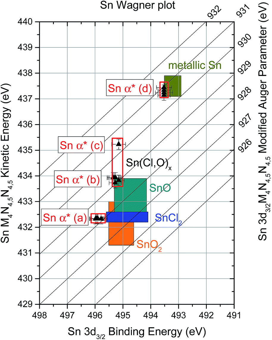 | ||
| Fig. 7 Sn modified Auger parameter (α*) of the investigated sample series in a Wagner plot format. Illustrated as shaded area are BE and KE values of reference Sn compounds reported in literature.30–36 | ||
The findings presented in this work highlight the effect that substrate conditions can exert on the chemical (and electronic) properties of the deposited material layers and have to be considered when optimizing the material as a precursor for Pb-free HOIP devices. The presence of O in the Mo-coated substrates may partly oxidize SnCl2 [resulting in the (potential) appearance of Sn(Cl,O)x phases] near the interface. However, the oxidation state of Sn in the formed tin oxide is still +2 avoiding the presence/formation of detrimental Sn4+ states. For perovskites using SnCl2 as an inorganic precursor deposited on the TiO2 substrate (e.g., in a two-step deposition method), similar results can be expected, which could lead to differences in morphology and crystallization of the deposited perovskite. Furthermore, it needs to be considered that metallic Sn is present in the deposited precursor film, which (if left unreacted) will act as deep defect and recombination center. However, it is highly probable that the small detected metallic Sn composition will readily react with the organic precursor (e.g., MAI) in the perovskite conversion step (i.e., second step of the two-step method),2–4 as evidenced by the absence of metallic Sn in the “25 s” sample. In the case of a (future) study of a fully-prepared Pb-free perovskite, additional structural information will be crucial to identify high-quality (i.e., single-phase) material.
Conclusions
The combined XPS/XAES and SEM characterization of a sample series of SnCl2 thin-films vapor deposited in UHV on Mo-coated substrates reveals the formation of up to four different Sn chemical environments and a Stranski–Krastanov type growth. The presence of O residues on the Mo-coated substrates likely acts as O source to oxidize SnCl2 and form Sn(Cl,O)x phases near the interface. Metallic Sn is also found to be present in all evaporation treatments. Similar results are expected for the deposition of SnCl2 on other O-containing substrate materials (e.g., TiO2) and thus need to be taken into account for precursor material optimization towards vacuum-based synthesis of Pb-free perovskites.Conflicts of interest
There are no conflicts to declare.Acknowledgements
RF, NLV, CH, RGW, and MB acknowledge funding from the Helmholtz Association (VH-NG-423).Notes and references
- http://www.nrel.gov/pv/assets/images/efficiency_chart.jpg.
- D. T. Moore, H. Sai, K. Wee Tan, L. A. Estroff and U. Wiesner, APL Mater., 2014, 2, 081802 CrossRef.
- B.-E. Cohen, S. Gamliel and L. Etgar, APL Mater., 2014, 2, 081502 CrossRef.
- J.-H. Im, I.-H. Jang, N. Pellet, M. Grätzel and N.-G. Park, Nat. Nanotechnol., 2014, 9, 927 CrossRef CAS PubMed.
- G. Niu, X. Guo and L. Wang, J. Mater. Chem. A, 2015, 3, 8970 CAS.
- T.-B. Song, Q. Chen, H. Zhou, C. Jiang, H.-H. Wang, Y. M. Yang, Y. Liu, J. You and Y. Yang, J. Mater. Chem. A, 2015, 3, 9032 CAS.
- X. Li, D. Bi, C. Yi, J.-D. Décoppet, J. Luo, S. M. Zakeeruddin, A. Hagfeldt and M. Grätzel, Science, 2016, 353, 58 CrossRef CAS PubMed.
- S. Shi, Y. Li, X. Li and H. Wang, Mater. Horiz., 2015, 2, 378 RSC.
- L. Fang, C. Xu, J. Li, O. K. Borggaard and D. Wang, Environ. Sci. Pollut. Res., 2017, 24, 9159 CrossRef CAS PubMed ; and references therein.
- C. C. Stoumpos, C. D. Malliakas and M. G. Kanatzidis, Inorg. Chem., 2013, 52, 9019 CrossRef CAS PubMed.
- F. Hao, C. C. Stoumpos, R. P. H. Chang and M. G. Kanatzidis, J. Am. Chem. Soc., 2014, 136, 8094 CrossRef CAS PubMed.
- F. Hao, C. C. Stoumpos, D. H. Cao, R. P. H. Chang and M. G. Kanatzidis, Nat. Photonics, 2014, 8, 489 CrossRef CAS.
- N. K. Noel, S. D. Stranks, A. Abate, C. Wehrenfennig, S. Guarnera, A.-A. Haghighirad, A. Sadhanala, G. E. Eperon, S. K. Pathak, M. B. Johnston, A. Petrozza, L. M. Herz and H. J. Snaith, Energy Environ. Sci., 2014, 7, 3061 CAS.
- Y. Ogomi, A. Morita, S. Tsukamoto, T. Saitho, N. Fujikawa, Q. Shen, T. Toyoda, K. Yoshino, S. S. Pandey, T. Ma and S. Hayase, J. Phys. Chem. Lett., 2014, 5, 1004 CrossRef CAS PubMed.
- Q. Chen, H. Zhou, Z. Hong, S. Luo, H.-S. Duan, H.-H. Wang, Y. Liu, G. Li and Y. Yang, J. Am. Chem. Soc., 2014, 136, 622 CrossRef CAS PubMed.
- K. Lips, T. F. Schulze, D. E. Starr, M. Bär, R. G. Wilks, F. Fenske, F. Ruske, M. Reiche, R. van de Krol, G. Reichardt, F. Schäfers, S. Hendel, R. Follath, J. Bahrdt, S. Peredkov, S. DeBeer, M. Hävecker, A. Knop-Gericke, B. Rau, C. A. Kaufmann, R. Schlatmann, R. Schlögl, B. Rech and S. Raoux, Proceedings of the 31st European Photovoltaic Solar Energy Conference and Exhibition, WIP, Hamburg, Munich, 2015 Search PubMed.
- Nonsequitur Technologies, Ion Guns: Model 1402-Low Energy Perfomance, 2017, http://nonsequitur-ion-gun.com/Model_1402.html.
- Dr Eberl MBE Komponenten, Source Clusters, 2017, http://www.mbe-komponenten.de/products/pdf/data-sheet-source-clusters.pdf.
- Scienta Omicron, Electron Spectrometers, 2017, http://www.scientaomicron.com/en/products/electron-spectrometer.
- PREVAC, X-ray Source RS40B1, 2017, https://www.prevac.eu/en/2,offer/37,instruments/119,x-ray-source-40b1.html.
- M. Wojdyr, J. Appl. Crystallogr., 2010, 43, 1126 CrossRef CAS.
- D. Briggs and M. P. Seah, Practical Surface Analysis by Auger and X-ray Photoelectron Spectroscopy, John Wiley & Sons, Chichester, New York, 1983 Search PubMed.
- Hitachi High-Technologies Corporation, MODEL S-4100 FIELD EMISSION SCANNING ELECTRON MICROSCOPE, 2002.
- S. Tougaard, QUASES-IMFP-TPP2M, 2002 Search PubMed.
- S. Tanuma, C. J. Powell and D. R. Penn, Surf. Interface Anal., 1994, 21, 165 CrossRef CAS.
- C. Argile and G. E. Rhead, Surf. Sci. Rep., 1989, 10, 277 CrossRef CAS.
- L. Baker, A. S. Cavanagh, J. Yin, S. M. George, A. Kongkanand and F. T. Wagner, Appl. Phys. Lett., 2012, 101, 111601 CrossRef.
- J. R. Dahn, R. L. Turner, O. Mao, R. A. Dunlap, A. E. George, M. M. Buckett, D. J. McClure and L. J. Krause, Thin Solid Films, 2002, 408, 111 CrossRef CAS.
- A. Bonakdarpour, K. C. Hewitt, T. D. Hatchard, M. D. Fleischauer and J. R. Dahn, Thin Solid Films, 2003, 440, 11 CrossRef CAS.
- J. F. Moulder, W. F. Stickle and P. E. Sobol, Handbook of X-ray Photoelectron Spectroscopy: A Reference Book of Standard Spectra for Identification and Interpretation of XPS Data, 2nd edn, Perkin-Elmer, Physical Electronics Division, 1995 Search PubMed.
- W.-K. Choi, H.-J. Jung and S.-K. Koh, J. Vac. Sci. Technol., 1996, 14, 359 CrossRef CAS.
- P. A. Grutsch, M. V. Zeller and T. P. Fehlner, Inorg. Chem., 1973, 12, 1431 CrossRef CAS.
- L. Kövér, Z. Kovács, R. Sanjinés, G. Moretti, I. Cserny, G. Margaritondo, J. Pálinkás and H. Adachi, Surf. Interface Anal., 1995, 23, 461 CrossRef.
- A. W. C. Lin, N. R. Armstrong and T. Kuwana, Anal. Chem., 1977, 49, 1228 CrossRef CAS.
- L. R. Pederson, Sol. Energy Mater., 1982, 6, 221 CrossRef CAS.
- C. D. Wagner, L. H. Gale and R. H. Raymond, Anal. Chem., 1979, 51, 466 CrossRef CAS.
- X. Liao, A. R. Jeong, R. G. Wilks, S. Wiesner, M. Rusu and M. Bär, J. Electron Spectrosc. Relat. Phenom., 2016, 212, 50 CrossRef CAS.
Footnotes |
| † Electronic supplementary information (ESI) available. See DOI: 10.1039/c7ra12172e |
| ‡ These authors contributed equally to this work. |
| § Although inorganic Sn compounds are considered safe for human applications, organic Sn compounds (especially mono-, di-, tri-, and tetrabutyltin and triphenyltin) are environmental pollutants posing severe dangers to aquatic ecosystems.9 |
| ¶ Note that in Fig. 3 after a SnCl2 effective thickness >3× IMFP values the increase/decrease of the signal trend lines plateau due to the information depth limit of XPS. For this reason, evaporation times showing saturated relative intensity values (i.e., 600 s and 800 s) cannot be used to directly determine the (effective) thickness of the deposited SnCl2 film (e.g., the “800 s” sample does not have a thickness of 15 IMFP values or ca. 34 nm). |
| This journal is © The Royal Society of Chemistry 2018 |