DOI:
10.1039/C7RA12058C
(Paper)
RSC Adv., 2018,
8, 3304-3311
Band gap engineering of SnS2 nanosheets by anion–anion codoping for visible-light photocatalysis
Received
2nd November 2017
, Accepted 27th December 2017
First published on 17th January 2018
Abstract
SnS2 nanosheets with three atom thickness have previously been synthesized and it has been shown that visible light absorption and hydrogen evolution through photocatalytic water splitting are restricted. In the present study, we have systematically investigated the electronic structures of anionic monodoped (N and P) and codoped (N–N, N–P, and P–P) SnS2 nanosheets for the design of efficient water redox photocatalysts by adopting first principles calculations with the hybrid HSE06 functional. The results show that the defect formation energies of both the anionic monodoped and all the codoped systems decrease monotonically with the decrease of the chemical potential of S. The P–P codoped SnS2 nanosheets are not only more favorable than other codoped systems under an S-poor condition, but they also reduce the band gap without introducing unoccupied impurity states above the Fermi level. Interestingly, although the P–P(ii) codoped system gives a band gap reduction, this system is only suitable for oxygen production and not for hydrogen evolution, which indicates that it may serve as a Z-scheme photocatalyst for water splitting. The P–P(i) codoped system may be a potential candidate for photocatalytic water splitting to generate hydrogen because of the appropriate band gap and band edge positions, which overcome the disadvantage that the pure SnS2 nanosheet is not beneficial for hydrogen production. More importantly, the result of optical absorption spectral analysis shows that the P–P(i) codoped SnS2 nanosheet absorbs a longer wavelength of the visible light spectrum as compared to the pristine SnS2 nanosheet. The P–P(I) codoped system with a lower doping concentration also has an absorption shift towards the visible light region.
1 Introduction
The search for sustainable and renewable energy has attracted extensive attention in the field of materials science over the last few decades because of energy exhaustion and environmental problems. Hydrogen is one of the most excellent energy carriers, and hydrogen production through photocatalytic water splitting under sunlight irradiation is a clean and promising approach for solving the energy issues.1–3 In order to make effective use of the visible light in the solar spectrum, the critical factor is that the photocatalyst should have suitable band gap and band edge positions.4,5 Therefore, band gap engineering is a significant issue for optimization of photocatalytic performance.
Recently, two-dimensional (2D) materials, such as SnS2,6–8 zinc oxide (ZnO),9–11 CdS,12 phosphorene,13 graphitic carbon nitrides (g-C3N4 (ref. 14) and g-C6N6 (ref. 15)), and transition metal dichalcogenides (TMDs),16,17 have attracted broad attention and have been widely applied in many fields because of their unusual properties. In particular, 2D materials with atomic thickness have two major advantages to promote the photocatalytic efficiency of water splitting, i.e. the larger surface areas available provide more photocatalytically active sites and shorter migration distance of carriers compared to bulk materials. Therefore, the use of 2D materials as photocatalysts has drawn tremendous research interest in both experiments and theoretical calculations for the design of high efficiency water redox photocatalysts.18–22 Among them, SnS2 with 2D structures including nanosheets, nanoparticles, and nanoplate, has been successfully synthesized in recent years.23–25 For example, Sun et al.24 have prepared monolayer SnS2 with three atom thickness and reported that the visible light conversion efficiency can approach 38.7%, which is much higher than that of bulk SnS2. Wei et al.25 have synthesized ultrathin SnS2 nanosheets, and have indicated that the photocatalytic activity has been significantly promoted because of the 2D sheet-like nanostructure. Zhuang et al.26 have also investigated the photocatalytic properties of SnS2 nanosheets, indicating that the overall water splitting can not spontaneously take place on the SnS2 nanosheet because of the influence of band edge positions (the valence band edge of the SnS2 nanosheet is more negative than the water oxidation potential level (O2/H2O), while the conduction band edge is lower than the water reduction potential level (H+/H2)). Therefore, it is necessary to adopt several strategies to modify the electronic structure and band edge positions of the SnS2 nanosheet.
Recently, in order to tune the optical, magnetic, and electronic properties, the doping of foreign elements into semiconductors has been carried out in many studies.27–29 For instance, Fe doped SnS2 nanosheets exhibit excellent visible light absorption behavior, and the optical absorption coefficient in the visible region increases monotonically with the increase of Fe doping concentration.27 Guo et al.28 have investigated the properties of ZnO nanosheets by doping with nonmetal atoms, which exhibit a nonmagnetic–antiferromagnetic–ferromagnetic transition. An et al.29 have prepared Cu-doped SnS2 nanosheets and observed that the visible-light photocatalytic activity is much higher than that of pure SnS2 nanosheets. However, monodoping usually introduces localized unoccupied states above the Fermi level, which accelerates the electron–hole recombination process.30 Besides, some vacancies which can trap charge carriers may form in these systems due to the charge imbalance.31 To overcome the above-described issues, the double-hole-mediated coupling of dopants has been found to be a promising strategy to enhance the visible light photocatalytic activity of semiconductor photocatalysts, such as SrTiO3,32 TiO2,33 NaTaO3,34 La2Ti2O7,35,36 Sr2Ta2O7, (ref. 37) etc. Wang et al.38 have successfully synthesized N–P codoped anatase TiO2 nanosheets and indicated that N–P codoping effectively reduced the band gap of TiO2 nanosheets from 3.20 to 2.48 eV. To the best of our knowledge, there are no theoretical reports on the effect of anion–anion double-hole-mediated codoping on the photocatalytic activity of SnS2 nanosheets.
In this work, by adopting density functional theory calculations, we have investigated if the anion–anion double-hole-mediated codoping of N–N, N–P, and P–P could effectively improve the photocatalytic activity and modify the electronic structure of SnS2 nanosheets. The structural geometries, defect formation energies, defect binding energies, electronic structures, band-edge alignment and optical properties of doped SnS2 nanosheets have been systematically investigated in our work. Finally, the effect of doping concentration on the electronic and optical properties of the SnS2 nanosheet has also been explored.
2 Computational method and process
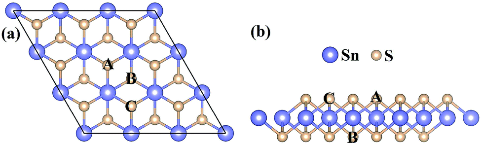
All calculations have been carried out using density functional theory (DFT) within the projector-augmented-wave (PAW) pseudopotentials39 implemented in the Vienna ab initio simulation package (VASP).40,41 The exchange correlation interactions are modeled by the Perdew–Burke–Ernzerhof (PBE)42 parameterization of the generalized gradient approximation (GGA).43 The valence electron configurations of Sn (4d105s25p2), S (3s23p4), N (2s22p3), and P (3s23p3) have been considered to construct the potentials in this work. The cutoff energy of 450 eV, the energy convergence tolerance of 1.0 × 10⁻⁵ eV, and the force convergence criteria of 0.01 eV Å−1 have been adopted to obtain the optimized geometry configurations. The vacuum space of 15 Å has been used to avoid interaction between the periodic images. The 3 × 3 × 1 and 5 × 5 × 1 Monkhorst–Pack44 k-point meshes have been used for the structural relaxation and electronic properties calculations, respectively. The SnS2 nanosheet has been constructed by a 3 × 3 × 1 supercell which contains 27 atoms. The calculated structural geometry of this supercell which has hexagonal structure is presented in Fig. 1. For monodoped SnS2 nanosheets, the nonmetal atoms (NM = N, P) have been adopted by replacing one S atom in the middle of the SnS2 nanosheet. For the N–N, N–P, and P–P codoped SnS2 nanosheets, there are two possible configurations: (i) two impurity atoms are used to replace two S atoms which are respectively located at A and B sites (see Fig. 1); (ii) two impurity atoms are used to substitute two S atoms which are located at A and C sites, respectively. In our work, we refer to them as N–N(i), N–P(i), P–P(i), N–N(ii), N–P(ii), and P–P(ii). Due to the PBE function having an underestimation of the band gaps of semiconductors, the Heyd–Scuseria–Ernzerhof (HSE06)45,46 hybrid functional, which is a more accurate and time-consuming approach, has been adopted to calculate the electronic and optical properties. The ion–core interaction consists of two parts in this functional: one for the short-range (SR), and one for the long-range (LR). The exchange–correlation energy is expressed as| | |
EHSEXC = χESRX(μ) + (1 − χ)EPBE,SRX(μ) + EPBE,LRX(μ) + EPBEC
| (1) |
where χ and μ stand for the mixing coefficient and the screening parameter, respectively. The mixing exchange parameter of 0.20 and screening parameter of 0.2 Å−1 are adopted in all calculations. In addition, the more reliable tetrahedron method with Blochl correction47 has been used to calculate the density of states (DOS) and projected density of states (PDOS).
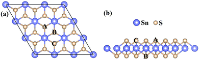 |
| | Fig. 1 The top view (a) and side view (b) of the 3 × 3 × 1 optimized supercell structure of the SnS2 nanosheet. | |
3 Results and discussion
3.1 The pristine SnS2 nanosheet
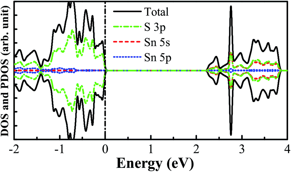
The pristine SnS2 nanosheet structure is cut from the (001) surface of the optimized SnS2 bulk structure. The 3 × 3 × 1 optimized supercell structure of the SnS2 nanosheet is indicated in Fig. 1. It possesses three atomic sublayers wherein the Sn atoms located in the center sublayer are bonded to the six nearest-neighboring S atoms which are located in the top and bottom sublayers. The optimized S–Sn distance is 2.582 Å which is larger than that (2.560 Å) in bulk SnS2, consistent with the previous theoretical and experimental results.48–50 The DOS and PDOS of the pure SnS2 nanosheet are presented in Fig. 2. It has been found that the pure SnS2 nanosheet is a non-magnetic semiconductor with a band gap of 2.24 eV. The PDOS analysis reveals that the valence band maximum (VBM) is mainly contributed to by S 3p states and the conduction band minimum (CBM) is dominated by the hybridization between S 3p and Sn 5s states. These calculated results agree well with the previous theoretical and experimental reports,49–51 which indicates the suitability of our calculation methods.
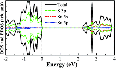 |
| | Fig. 2 The calculated DOS and PDOS for the pure SnS2 nanosheet. The vertical black dashed line represents the Fermi level. | |
3.2 Monodoped SnS2 nanosheets
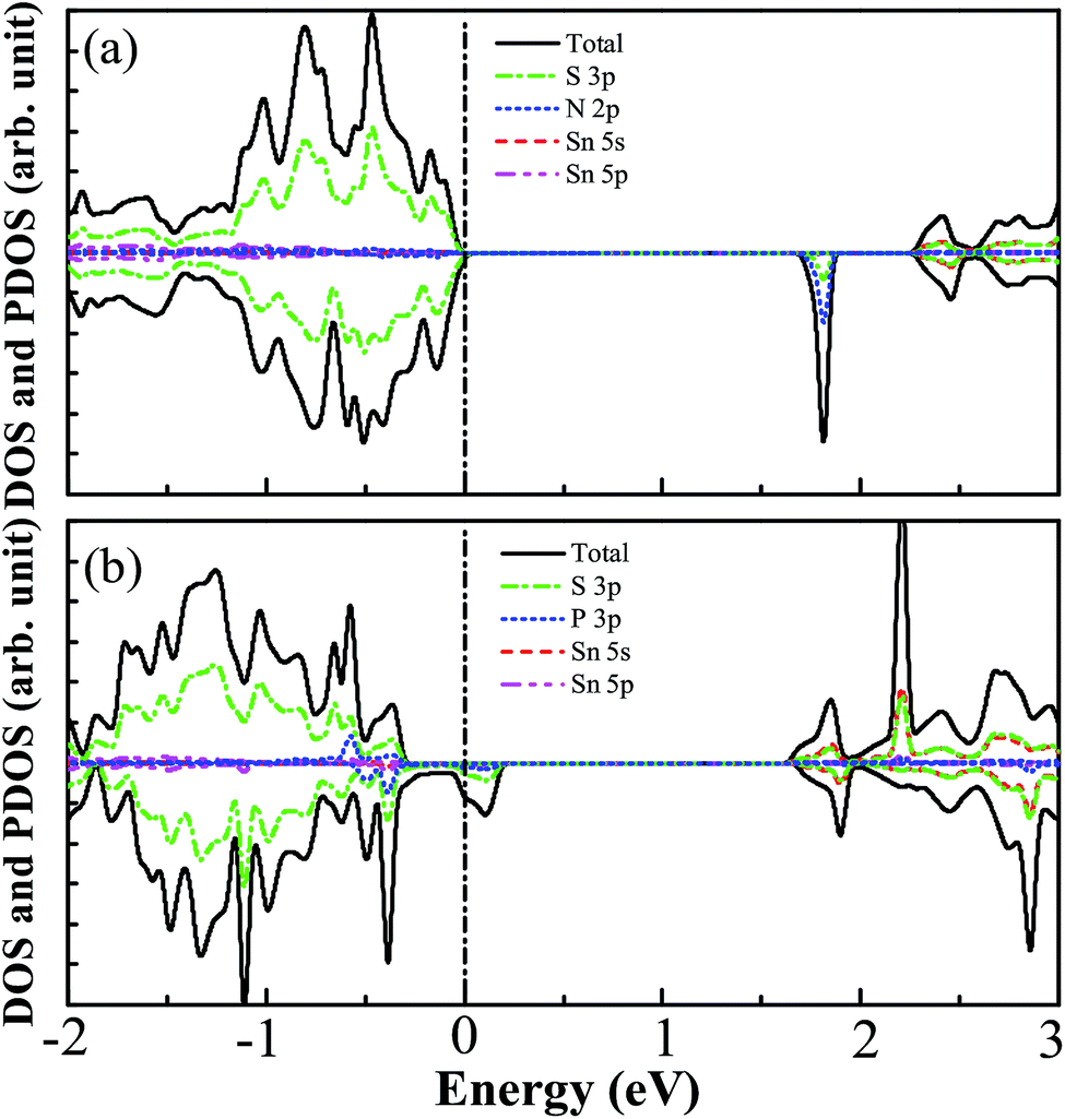
For the N monodoped SnS2 nanosheet, the bond distance between the N atom and the nearest-neighboring Sn atom is 2.203 Å, which is obviously shorter than the length of the S–Sn bonds in the pristine SnS2 nanosheet. This is due to the stronger Coulomb interaction between the N and Sn atoms than that between the S and Sn atoms in the pure system, which can be demonstrated by the result of Bader charge analysis, showing that the charge transfer (1.02 eV) from Sn to N is larger than that (0.77 eV) from Sn to S in the pure system. For the P monodoped system, the bond length between the P atom and the nearest-neighboring Sn atom is 2.617 Å, which is close to that of the Sn–S bonds in the SnS2 nanosheet but much larger than the distance of the N–Sn bonds in the N monodoped SnS2 nanosheet, which may be explained by the small difference in the ionic radius between the P dopant and S atom. In order to investigate the effect of monodoping with N and P dopants on the characteristics of the electronic structure of the SnS2 nanosheet, we have calculated the DOS and PDOS of monodoped systems, indicated in Fig. 3. As shown in Fig. 3(a), it can be seen that the VBM is mainly dominated by S 3p states while the CBM is mainly contributed to by the S 3p and Sn 5s states for the N monodoped SnS2 nanosheet. Interestingly, there are no N 2p states near the VBM, which is different from the previous studies, such as with N doped-TiO2,33 SrTiO3,32 and ZrO2.52 This is because the N 2p orbital energy is lower than the S 3p orbital energy. In addition, the impurity states close to the conduction band of the SnS2 nanosheet are derived from the hybridization between the N 2p states and S 3p states. Here, we define that the effective band gap is the energy difference between the impurity states and the VBM, which is calculated as 1.70 eV, which is good for the visible light absorption. However, the empty states in the band gap may trap the photoexcited carriers and promote electron–hole recombination, which is harmful for the photocatalytic reaction. The DOS and PDOS for the P doped system are displayed in Fig. 3(b), indicating that such empty states appear above the Fermi level and that the impurity states are contributed to by P 3p and S 3p states.
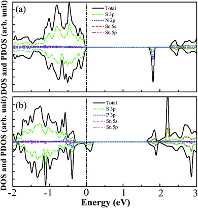 |
| | Fig. 3 The calculated DOS and PDOS of SnS2 nanosheets with (a) N and (b) P monodoping. The vertical dashed line indicates the Fermi level. | |
3.3 Anion–anion codoped SnS2 nanosheets
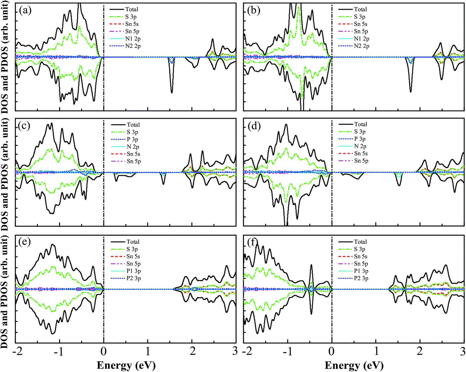
The DOS and PDOS for N–N(i), N–N(ii), N–P(i), N–P(ii), P–P(i), and P–P(ii) codoped SnS2 nanosheets are displayed in Fig. 4(a)–(f). For the N–N(i) codoped case, the VBM is mainly contributed to by S 3p states with a little of the N 2p states, while the CBM is mainly composed of the S 3p and Sn 5s states. Some unoccupied impurity states are found to appear above the Fermi level, which is different from the previous reports, such as with N–N codoped TiO2,33 SrTiO3,32 and NaTaO3.34 This is because the N–N coupling does not happen in this system. Furthermore, these impurity states may accelerate the recombination of photogenerated charge carriers and suppress the photocatalytic activity,11,30 indicating that the N–N(i) codoped system is not a promising candidate for visible light photocatalysis. For the case of N–N(ii) codoping, the VBM is mainly dominated by S 3p states and the CBM consists mainly of S 3p and Sn 5s states. It is clearly seen that some unfilled impurity states which originate from the mixing of N 2p and S 3p states appear in the band gap, which indicates that N–N(ii) codoped SnS2 nanosheets are not suitable for visible light photocatalysis. For the N–P(i) and N–P(ii) codoped systems, the DOS and PDOS for them are plotted in Fig. 4(c) and (d), respectively, indicating that the VBMs for them are both mainly contributed to by S 3p states with a slight amount of N 2p states, while the CBMs are both mainly dominated by the S 3p and Sn 5s states. However, though the band gaps for N–P(i) and N–P(ii) codoped SnS2 nanosheets are 1.78 eV and 1.90 eV, respectively, both codoped systems suffer from partially unoccupied states appearing above the Fermi level, which can increase electron–hole recombination and have a negative influence on the photocatalytic activity. The characteristics of the DOS and PDOS of P–P(i) and P–P(ii) codoped systems are respectively presented in Fig. 4(e) and (f). It is found that the VBMs of both systems are still mainly dominated by S 3p states, while the CBMs are both mainly contributed to by the mixtures between S 3p and Sn 5s states. The calculated band gaps of P–P(i) and P–P(ii) codoped SnS2 nanosheets are 1.62 eV and 1.29 eV, respectively. Interestingly, there are no unoccupied impurity states in the band gaps of both systems, which should be attributed to the strong coupling between the P1 and P2 atoms. Due to the existence of one unpaired electron for the P1 and P2 atoms, when the two atoms are close to each other the unpaired 3p electrons of two P atoms hybridise with each other and form a bonding state and anti-bonding state. Therefore, the P–P(i) and P–P(ii) codoped SnS2 nanosheets may be excellent candidates for visible light photocatalysis.
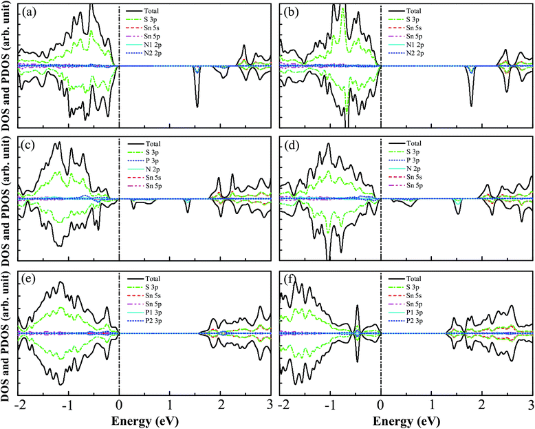 |
| | Fig. 4 The calculated DOS and PDOS for (a) N–N(i), (b) N–N(ii), (c) N–P(i), (d) N–P(ii), (e) P–P(i), and (f) P–P(ii) codoped SnS2 nanosheets. The black dashed line denotes the Fermi level. | |
3.4 Defect formation energy
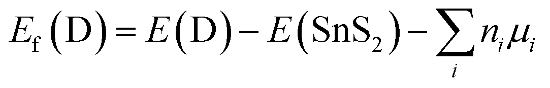
In order to search for the favorable synthetic conditions of doped SnS2 nanosheets, the defect formation energy (Ef) has been determined by adopting the following equation53,54| |
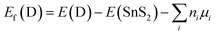 | (2) |
where E(D) and E(SnS2) stand for the total energies of the doped and pure SnS2 nanosheets, respectively, ni is the number of atoms removed (ni < 0) or added (ni > 0) to the pure system for the construction of doped SnS2 nanosheets, while μi is the chemical potential of the corresponding atom and the value of μi depends on the synthetic environment. Under the conditions of equilibrium between the SnS2 nanosheet and the reservoir of Sn and S atoms, the chemical potential of the constituent elements must follow the relation:| | |
μSn + 2μS = μSnS2(monolayer)
| (3) |
where μSnS2(monolayer) is the chemical potential of the SnS2 monolayer, which is obtained from the total energy of the SnS2 monolayer per unit cell. The chemical potential of Sn and S can not exceed that of the Sn bulk (μSn(bulk)) and S gas (μS(gas)), thus the following relationships must be obeyed:| | |
μminSn ≤ μSn ≤ μSn(bulk)
| (4) |
Moreover, in order to form the SnS2 nanosheet spontaneously, the minima of μSn and μS satisfy
| | |
μminSn = E(SnnS2n) − E(Snn−1S2n)
| (6) |
| | |
μminS = E(SnnS2n) − E(SnnS2n−1)
| (7) |
where
E(Sn
nSn
2n),
E(Sn
n−1Sn
2n), and
E(Sn
nSn
2n−1) are, respectively, the total energies of Sn
nSn
2n systems constructed by
n primitive cells without and with Sn and S defects. In order to facilitate discussion, we set Δ
μSn =
μSn −
μSn(bulk) and Δ
μS =
μS −
μS(gas) for this work. For dopants, we suppose that N
2 and P
4 molecules act as N and P reservoirs, respectively. The defect formation energies of doped SnS
2 nanosheets as a function of Δ
μS have been calculated, and are presented in
Fig. 5. In addition, the minimum defect formation energies of different doped systems are summarized in
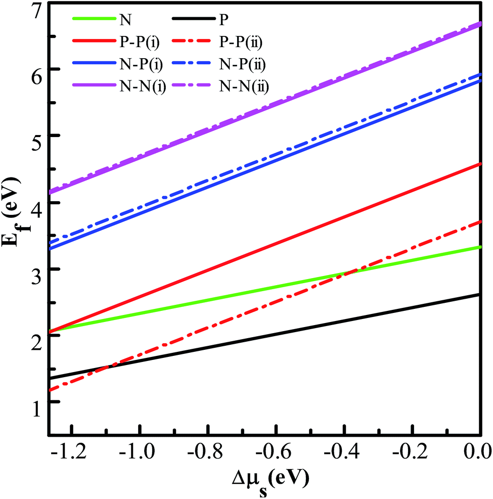
Table 1. As shown in
Fig. 5, it can be seen that the defect formation energies of both the NM-monodoped and all the codoped systems increase monotonically with the increase of the chemical potential of S. It is energetically favorable to form N (P)-monodoped and all codoped SnS
2 nanosheets under an S-poor condition. This is because the vacancy which plays an indispensable role for alternative doping is easily formed under an S-poor growth condition. Moreover, the P–P codoped systems have lower defect formation energies than other codoped configurations, which indicates that P–P codoped SnS
2 nanosheets are feasible experimentally. Here, in order to discuss the relative stability of codoped SnS
2 nanosheets with respect to the monodoped systems, we have also calculated the defect pair binding energies of codoped systems. The defect binding energies of N–N (
Eb(N + N)), N–P (
Eb(N + P)), and P–P (
Eb(P + P)) codoped SnS
2 nanosheets are calculated by adopting the following equations, respectively:
| | |
Eb(N + N) = 2E(N) − E(pure) − E(N + N)
| (8) |
| | |
Eb(N + P) = E(N) + E(P) − E(pure) − E(N + P)
| (9) |
| | |
Eb(P + P) = 2E(P) − E(pure) − E(P + P)
| (10) |
where
E(pure),
E(P),
E(N),
E(N + N),
E(N + P), and
E(P + P) are the total energies of pure, P monodoped, N monodoped, N–N codoped, N–P codoped, and P–P codoped systems with the same supercell, respectively. As shown in
Table 1, the defect binding energies of the N–P and P–P codoped systems are positive and that of the N–N codoped system is negative, which means that the N–P and P–P codoped systems are energetically favorable and the N–N codoped system is unfavorable in energy in comparison with the corresponding monodoped SnS
2 nanosheet. This is because of the strong Coulomb interaction between the dopants and the Sn atoms in the N–P and P–P codoped systems.
 |
| | Fig. 5 The calculated defect formation energies as a function of the chemical potential of S for the doped SnS2 nanosheets. | |
Table 1 The calculated minimum defect formation energies (Ef), the defect binding energies (Eb), and the corresponding chemical potentials of S and Sn for the doped systems. All the units are in eV
| Structure |
Ef |
Eb |
ΔμS |
ΔμSn |
| N |
2.06 |
— |
−1.27 |
−2.53 |
| P |
1.35 |
— |
−1.27 |
−2.53 |
| N–N(i) |
4.13 |
−0.02 |
−1.27 |
−2.53 |
| N–N(ii) |
4.16 |
−0.05 |
−1.27 |
−2.53 |
| N–P(i) |
3.30 |
0.11 |
−1.27 |
−2.53 |
| N–P(ii) |
3.39 |
0.02 |
−1.27 |
−2.53 |
| P–P(i) |
2.04 |
0.65 |
−1.27 |
−2.53 |
| P–P(ii) |
1.18 |
1.52 |
−1.27 |
−2.53 |
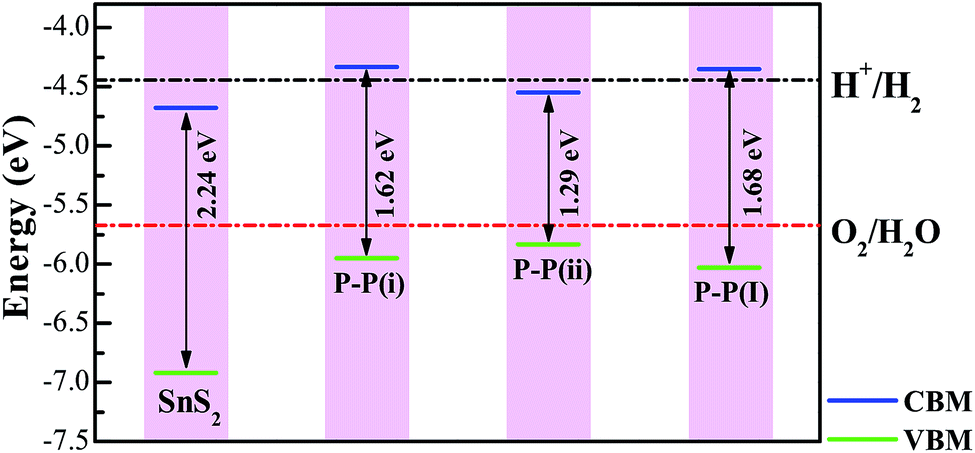
3.5 Band edge alignment
It is well known that an excellent photocatalyst should not only have an appropriate band gap, but also suitable band edge positions, i.e. the water reduction level and oxidation level must lie between the CB edge and VB edge so that both the hydrogen evolution reaction and oxygen evolution reaction become thermodynamically allowed. On the basis of the band edge positions, some photocatalysts are suitable for only hydrogen evolution and some photocatalysts are good for only oxygen evolution, which is called the Z-scheme photocatalysis system. Here, we have considered the situation of the standard water reduction level (−4.44 eV) and oxidation level (−5.67 eV) with respect to the vacuum level.55 A large vacuum space has been used to calculate the absolute position of the band edge for quantitatively comparing with the water redox potentials. As the calculated vacuum level (by averaging the LOCPOT file along the specified plane from VASP) is a relative value, we have shifted the energy value of the CBM (VBM) for each system by subtracting this value to obtain the absolute band edge position.
The calculated positions of the CBM and VBM of the pure and doped SnS2 nanosheets with respect to the standard hydrogen electrode potentials are indicated in Fig. 6. For the doped systems, the P–P(i) and P–P(ii) codoped SnS2 nanosheets have been considered in this work, as these cases result in significant reductions of the band gaps without introducing impurity states above the Fermi level. Apparently, the VBM of the pure SnS2 nanosheet is below the oxidation potential of H2O/O2, while the CBM is also lower than the reduction potential of H+/H2, which indicates that the pure SnS2 nanosheet is suitable for only oxygen production but not for hydrogen production, in good agreement with the previous theoretical reports.20,56,57 For the P–P(ii) codoped system, the VBM lies across the oxidation level of water and the CBM is below the reduction level of water, indicating that it is not beneficial for hydrogen production. However, this system may be considered as a Z-scheme type photocatalyst for oxygen production. For the P–P(i) codoped SnS2 nanosheet, the VBM is more negative than the water oxidation level and the CBM is higher than the water reduction level, which shows that this system is favorable for both the photo-reduction and photo-oxidation of water. Thus, the P–P(i) codoped SnS2 nanosheet is expected to be a promising candidate for hydrogen evolution from overall water splitting under visible light radiation.
 |
| | Fig. 6 The calculated VBM and CBM positions of pure and codoped SnS2 nanosheets with respect to the water redox potentials. | |
3.6 Optical properties
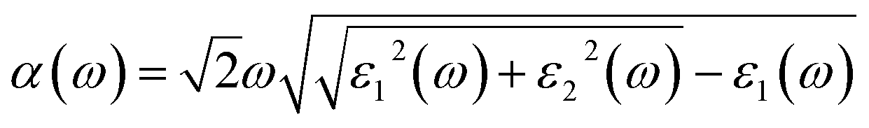
Optical properties play a critical role in evaluating the performance of photocatalysts in the visible light region. Thus, we have further investigated the optical absorption spectra of the P–P(i) codoped and pure SnS2 nanosheets. The P–P(i) codoped system has been considered, as it has a suitable band gap without introducing impurity states above the Fermi level and band edge positions. The absorption coefficient α(ω) satisfies the following relation58| |
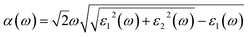 | (11) |
where ε1(ω) is the real part which is obtained using the Kramers–Kronig transformation, and ε2(ω) is the imaginary part which has been calculated by summing over a large amount of empty states. Fig. 7 displays the calculated absorption coefficient of pure and codoped SnS2 nanosheets. It indicates that the P–P(i) codoped SnS2 nanosheet can harvest a longer wavelength of the visible light spectrum compared to the pure SnS2 nanosheet for visible light photocatalysis, which can be attributed to the reasonable band gap reduction.
 |
| | Fig. 7 The optical absorption spectra of pure and codoped SnS2 nanosheets. | |
3.7 Effect of concentration
In order to investigate the effect of the doping concentration on the band gap, the electronic structure of the P–P(i) codoped SnS2 nanosheet has been calculated by using a larger 4 × 4 × 1 supercell containing a total of 48 atoms, as this configuration has an appropriate band edge position and a suitable band gap without introducing impurity states above the Fermi level. The concentration of dopant corresponds to 4.17 at%. For the sake of discussion, we refer to it as P–P(I) in this work. The calculated minimum defect formation energy for the P–P(I) codoped system is 2.04 eV, which is the same as that of the P–P(i) codoped SnS2 nanosheet. This indicates that the defect formation energy is hardly affected by the increase of the supercell size. The calculated DOS and PDOS of the P–P(I) codoped SnS2 nanosheet is presented in Fig. 8, which shows that the VBM is mainly dominated by S 3p states and the CBM is mainly composed of S 3p and Sn 5s states. The calculated band gap of this system is 1.68 eV. As shown in Fig. 6, the water reduction level and oxidation level lie between the CBM and VBM of the P–P(I) codoped SnS2 nanosheet, manifesting that this system is favorable for water splitting. On the other hand, the calculated absorption curve of the P–P(I) codoped system is shown in Fig. 7, which displays that an absorption shift towards the visible region is quite significant even at a lower concentration of dopant element.
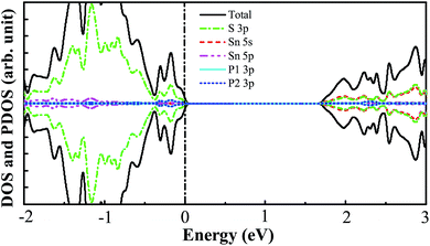 |
| | Fig. 8 The calculated DOS and PDOS of the P–P(I) codoped SnS2 nanosheet. The vertical dashed line indicates the Fermi level. | |
4 Conclusion
We have employed hybrid density functional calculations to systematically investigate the electronic structures of anionic monodoped (N and P) and codoped (N–N, N–P, and P–P) SnS2 nanosheets for the design of efficient water redox photocatalysts. The calculated results show that the defect formation energies of both the anionic monodoped and all the codoped systems decrease monotonically with the decrease of the chemical potential of S. The P–P codoped SnS2 nanosheets are not only more favorable than other codoped systems under an S-poor condition, but they also have a reduced band gap without introducing unoccupied impurity states above the Fermi level. Though the P–P(ii) codoped system gives a band gap reduction, this system is only suitable for oxygen evolution and not for hydrogen evolution, and thus it may serve as a Z-scheme photocatalyst for water splitting. The P–P(i) codoped system may be a potential candidate for photocatalytic water splitting to generate hydrogen because of the appropriate band gap and band edge positions, which overcome the disadvantage that the pure SnS2 nanosheet is not beneficial for hydrogen production. More importantly, the result of the optical absorption spectral analysis shows that the P–P(i) codoped SnS2 nanosheet absorbs a longer wavelength of the visible light spectrum as compared to the pristine SnS2 nanosheet. The P–P(I) codoped system has an absorption shift toward the visible region even at a lower doping concentration.
Conflicts of interest
There are no conflicts to declare.
Acknowledgements
This work was supported by the Natural Science Foundation of Chongqing under Grant No. CSTC-2017jcyjBX0035.
References
- A. Kudo and Y. Miseki, Chem. Soc. Rev., 2009, 38, 253–278 RSC.
- G. Wang, H. Yuan, A. Kuang, W. Hu, G. Zhang and H. Chen, Int. J. Hydrogen Energy, 2014, 39, 3780–3789 CrossRef CAS.
- S. J. A. Moniz, S. A. Shevlin, D. J. Martin, Z. X. Guo and J. W. Tang, Energy Environ. Sci., 2015, 8, 731–759 CAS.
- Y. Gai, J. Li, S. S. Li, J. B. Xia and S. H. Wei, Phys. Rev. Lett., 2009, 102, 36402 CrossRef PubMed.
- O. Khaselev and J. A. Turner, Science, 1998, 280, 425–427 CrossRef CAS PubMed.
- D. M. Guzman and A. Strachan, J. Appl. Phys., 2014, 115, 243701 CrossRef.
- H. Zhong, G. Yang, H. Song, Q. Liao, H. Cui, P. Shen and C. Wang, J. Phys. Chem. C, 2012, 116, 9319–9326 CAS.
- J. Liu and E. Hua, J. Phys. Chem. C, 2017, 121, 25827–25835 CAS.
- C. Tusche, H. L. Meyerheim and J. Kirschner, Phys. Rev. Lett., 2007, 99, 026102 CrossRef CAS PubMed.
- F. Claeyssens, C. L. Freeman, N. L. Allan, Y. Sun, M. N. R. Ashfold and J. H. Harding, J. Mater. Chem., 2005, 15, 139–148 RSC.
- X. Luo, G. Wang, Y. Huang, B. Wang, H. Yuan and H. Chen, J. Phys. Chem. C, 2017, 121, 18534–18543 CAS.
- J. Wang, J. Meng, Q. Li and J. Yang, Phys. Chem. Chem. Phys., 2016, 18, 17029–17036 RSC.
- J. Kim, S. S. Baik, S. H. Ryu, Y. Sohn, S. Park, B.-G. Park, J. Denlinger, Y. Yi, H. J. Choi and K. S. Kim, Science, 2015, 349, 723 CrossRef CAS PubMed.
- X. Wang, K. Maeda, X. Chen, K. Takanabe, K. Domen, Y. Hou, X. Fu and M. Antonietti, J. Am. Chem. Soc., 2009, 131, 1680–1681 CrossRef CAS PubMed.
- K. Srinivasu, B. Modak and S. K. Ghosh, J. Phys. Chem. C, 2014, 118, 26479–26484 CAS.
- C. Ataca, H. Sahin and S. Ciraci, J. Phys. Chem. C, 2012, 116, 8983–8999 CAS.
- Q. H. Wang, K. K. Zadeh, A. Kis, J. N. Coleman and M. S. Strano, Nat. Nanotechnol., 2012, 7, 699–712 CrossRef CAS PubMed.
- Y. F. Sun, Z. H. Sun, S. Gao, H. Cheng, Q. H. Liu, J. Y. Piao, T. Yao, C. Z. Wu, S. L. Hu, S. Q. Wei and Y. Xie, Nat. Commun., 2012, 3, 1057 CrossRef PubMed.
- Y. G. Li, Y. L. Li, C. M. Araujo, W. Luo and R. Ahuja, Catal. Sci. Technol., 2013, 3, 2214–2220 CAS.
- H. L. Zhuang and R. G. Hennig, Chem. Mater., 2013, 25, 3232–3238 CrossRef CAS.
- B. Luo, G. Liu and L. Z. Wang, Nanoscale, 2016, 8, 6904–6920 RSC.
- Y. Bai, Q. Zhang, G. Luo, Y. Bu, L. Fan and B. Wang, Phys. Chem. Chem. Phys., 2017, 19, 15394 RSC.
- J. Seo, J. Jang, S. Park, C. Kim, B. Park and J. Cheon, Adv. Mater., 2008, 20, 4269 CrossRef CAS.
- Y. Sun, H. Cheng, S. Gao, Z. Sun, Q. Liu, Q. Liu, F. Lei, T. Yao, J. He, S. Wei and Y. Xie, Angew. Chem., Int. Ed., 2012, 51, 8727 CrossRef CAS PubMed.
- R. Wei, J. Hu, T. Zhou, X. Zhou, J. Liu and J. Li, Acta Mater., 2014, 66, 163–171 CrossRef CAS.
- H. L. Zhuang and R. G. Hennig, Phys. Rev. B: Condens. Matter Mater. Phys., 2013, 88, 115314 CrossRef.
- Y. M. Liu, F. Wang, D. C. Kong, B. Hu, C. X. Xia and J. X. Su, Phys. Lett. A, 2017, 381, 1732–1737 CrossRef CAS.
- H. Guo, Y. Zhao, N. Lu, E. Kan, X. C. Zeng, X. Wu and J. Yang, J. Phys. Chem. C, 2012, 116, 11336–11342 CAS.
- X. An, C. Y. Jimmy and J. Tang, J. Mater. Chem. A, 2014, 2, 1000–1005 CAS.
- G. Wang, H. Chen, Y. Li, A. Kuang, H. Yuan and G. Wu, Phys. Chem. Chem. Phys., 2015, 17, 28743–28753 RSC.
- Z. Lin, A. Orlov, R. M. Lambert and M. C. Payne, J. Phys. Chem. B, 2005, 109, 20948–20952 CrossRef CAS PubMed.
- P. Liu, J. Nisar, B. Pathak and R. Ahuja, Int. J. Hydrogen Energy, 2012, 16, 11611–11617 CrossRef.
- W.-J. Yin, S.-H. Wei, M. M. Al-Jassim and Y. Yan, Phys. Rev. Lett., 2011, 106, 066801 CrossRef PubMed.
- B. Wang, P. D. Kanhere, Z. Chen, J. Nisar, B. Pathak and R. Ahuja, J. Phys. Chem. C, 2013, 44, 22518–22524 Search PubMed.
- P. Liu, J. Nisar, B. Sa, B. Pathak and R. Ahuja, J. Phys. Chem. C, 2013, 117, 13845–13852 CAS.
- P. Liu, J. Nisar, B. Pathak and R. Ahuja, Phys. Chem. Chem. Phys., 2013, 15, 17150–17157 RSC.
- P. Liu, J. Nisar, R. Ahuja and B. Pathak, J. Phys. Chem. C, 2013, 117, 5043–5050 CAS.
- F. Wang, P.-P. Ban, J. P. Parry, X.-H. Xu and H. Zeng, Rare Met., 2016, 35, 940–947 CrossRef CAS.
- P. E. Blochl, Phys. Rev. B: Condens. Matter Mater. Phys., 1994, 50, 17953–17979 CrossRef.
- G. Kresse and D. Joubert, Phys. Rev. B: Condens. Matter Mater. Phys., 1999, 59, 1758–1775 CrossRef CAS.
- G. Kresse and J. Furthmuller, Phys. Rev. B: Condens. Matter Mater. Phys., 1996, 54, 11169–11186 CrossRef CAS.
- M. Ernzerhof and G. E. Scuseria, J. Chem. Phys., 1999, 110, 5029–5036 CrossRef CAS.
- J. A. White and D. M. Bird, Phys. Rev. B: Condens. Matter Mater. Phys., 1994, 50, 4954–4957 CrossRef CAS.
- H. J. Monkhorst and J. D. Pack, Phys. Rev. B: Solid State, 1976, 13, 5188–5192 CrossRef.
- J. Heyd, G. E. Scuseria and M. Ernzerhof, J. Chem. Phys., 2003, 118, 8207–8215 CrossRef CAS.
- J. Heyd, G. E. Scuseria and M. Ernzerhof, J. Chem. Phys., 2006, 124, 219906 CrossRef.
- P. E. Blochl, O. Jepsen and O. K. Andersen, Phys. Rev. B: Condens. Matter Mater. Phys., 1994, 49, 16223–16233 CrossRef CAS.
- M. L. Toh, K. J. Tan, F. X. Wei, K. K. Zhang, H. Jiang and C. Kloc, J. Solid State Chem., 2013, 198, 224–230 CrossRef CAS.
- Y. Seminovski, P. Palacios and P. Wahnon, Thin Solid Films, 2013, 535, 387–389 CrossRef CAS.
- C. X. Xia, Y. T. Peng, H. Zhang, T. X. Wang, S. Y. Wei and Y. Jia, Phys. Chem. Chem. Phys., 2014, 16, 19674 RSC.
- S. K. Arora, D. H. Patel and M. K. Agarwal, Cryst. Res. Technol., 1993, 28, 623–627 CrossRef CAS.
- J. Wang, J. Huang, J. Meng, Q. Li and J. Yang, Phys. Chem. Chem. Phys., 2016, 18, 17517–17524 RSC.
- C. W. M. Castleton, A. Hoglund and S. Mirbt, Phys. Rev. B: Condens. Matter Mater. Phys., 2006, 73, 035215 CrossRef.
- C. G. V. de Walle and J. Neugebauer, J. Appl. Phys., 2004, 95, 3851–3879 CrossRef.
- V. Chakrapani, J. C. Angus, A. B. Anderson, S. D. Wolter, B. R. Stoner and G. U. Sumanasekera, Science, 2007, 318, 1424 CrossRef CAS PubMed.
- D. Yu, Y. Liu, L. Sun, P. Wu and W. Zhou, Phys. Chem. Chem. Phys., 2016, 18, 318–324 RSC.
- L. Sun, W. Zhou, Y. Liu, D. Yu and P. Wu, Appl. Surf. Sci., 2016, 389, 484–490 CrossRef CAS.
- S. Saha and T. P. Sinha, Phys. Rev. B: Condens. Matter Mater. Phys., 2000, 62, 8828–8834 CrossRef CAS.
|
| This journal is © The Royal Society of Chemistry 2018 |
Click here to see how this site uses Cookies. View our privacy policy here. 
 Open Access Article
 This Open Access Article is licensed under a Creative Commons Attribution-Non Commercial 3.0 Unported Licence
 ,
Hong Chen
,
Hong Chen