
 Open Access Article
 This Open Access Article is licensed under a Creative Commons Attribution-Non Commercial 3.0 Unported Licence
Ultrawide range tuning of direct band gap in MgZnO monolayer via electric field effect
Hongfei Chen a,
Changlong Tan*a,
Dan Suna,
Wenbin Zhaoa,
Xiaohua Tiana and
Yuewu Huangb
a,
Changlong Tan*a,
Dan Suna,
Wenbin Zhaoa,
Xiaohua Tiana and
Yuewu Huangb
aCollege of Applied Science, Harbin University of Science and Technology, Harbin 150080, China. E-mail: changlongtan@hrbust.edu.cn; Tel: +86-451-8639-0728
bSchool of Materials Science and Engineering, Harbin Institute of Technology, Harbin 150001, China
First published on 3rd January 2018
Abstract
Two-dimensional (2D) materials are building blocks for the next generation of electronic and optoelectronic devices. Tuning band gap in 2D materials over a broad range from ultraviolet to infrared is of scientific and technological importance for a wide range of applications, but its execution remains a challenge. Herein, tuning the band gap from 5.27 eV to 0.69 eV has been realized by utilizing an external electric field. Interestingly, under external electric field the MgZnO monolayer remains a direct band gap semiconductor, which has clear advantage for applications in optical devices. Moreover, the external electric field significantly leads to a red shift of the optical absorption peaks. The absorption coefficients and reflectivity decrease with increase in the external electric field in MgZnO monolayer. These findings should render these materials suitable for future applications in electronic and optoelectronic devices.
1. Introduction
Energy band gap plays a crucial role in the operation of semiconductor devices such as p–n junctions, transistors, and sensors.1–3 The tunable band gap is a highly desirable method to flexibly optimize performance of these devices. A narrow band gap greatly restricts their applications, particularly in optoelectronic devices with photoresponse in the blue and UV range. Therefore, band engineering is really important to the semiconductor materials.Zinc oxide (ZnO) has emerged as a promising semiconductor material with a wide direct band gap of 3.37 eV and a large exciton binding energy of 60 meV at room temperature.4 These features make it widely useful in photoelectric applications, such as transparent conductive oxides, light emitting devices and gas sensors.5–11 The successful fabrication of graphene in 2004 (ref. 12) led to new research in two-dimensional (2D) materials. These 2D materials exhibit diverse electronic properties due to quantum confinement in different dimensions, and have drawn the attention of the scientific community for extensive investigations.13–16 Doping is one of the best approaches to enhance electronic and optical properties of the materials. In our previous study, we discovered that there is a monotonous increase in the band gap with an increase in Mg concentration, and a direct band gap transition is always observed for MgZnO monolayer when Mg concentration is less than 50 at%.17
For the layered TMDs' applications in optoelectronics, tunable electronic properties are crucial. If the band gap can be tuned, meaning that a semiconductor with a lower band gap or a semiconductor-to-metal transition can be obtained, nanodevices with a wide range of tunable band gaps may be fabricated. Wu et al. investigated the energy gap modulation by the size of width under the transverse electric field.18 The band gap variation behaviors have been observed for the Si nanosheets subject to symmetrical and asymmetrical strains by Zhang et al.19 There are numerous strategies that have been proposed for band gap engineering in 2D materials such as doping some outer atoms, introducing nano-holes or applying strain. We have found that the use of external electric fields is one of the most effective methods to tune the band gap since electric gates are easy to set up and the effective strength is readily controlled by varying the bias between gates.20–23 Herein, we explored the possibility of using electric field to manipulate the electronic band structures of Mg-doped ZnO. The dopant concentration of Mg is 50 at%. Our results indicate that electric field can tune not only the magnitude of the band gap, but also the band dispersion. The wide range tuning direct band gap from 5.27 eV to 0.69 eV has been realized by external electric field, which has crucial implications for the applications of MgZnO monolayer in optoelectronics, luminescence, and solar cells.
2. Calculation methods
Our first principles calculations are based on the density functional theory (DFT) within a generalized gradient approximation (GGA). The calculations were performed using the CASTEP24 package with ultrasoft pseudo potentials by the Material Studios 8.0. The package is an ab initio quantum-mechanic code based on DFT.25 For each supercell, a vacuum region of 15 Å along the surface normal was set to ensure the cancellation of spurious interactions between periodic images. All the calculations were carried out with spin-polarization. The plane-wave cutoff energy was set at 380 eV and the Brillouin zone was sampled with 4 × 4 × 1 Monkhorst–Pack grid.26 All the structures were fully relaxed and the optimization was completed when the total energy and the maximum force converge to 10−6 eV per atom and 0.02 eV Å−1, respectively. The standard density functional theory underestimates the band gap of numerous transition metal oxides. To obtain a more accurate representation of the electronic structure of ZnO, we adopt the DFT + U method, in which the Hubbard parameter U is added to both Zn 3d and O 2p orbits (UZn,d = 10 eV and UO,p = 7 eV). This was also used in our previous study.27 The calculated band gap (3.37 eV) is in good agreement with the experimental results.283. Results and discussion
3.1 Structural properties
In this study, we investigated an optimized 2 × 2 × 1 supercell of ZnO monolayer with two Zn atoms replaced by two Mg atoms. The atomic structure of 2D ZnO monolayer was cut from initial bulk ZnO (0001) plane; the optimized structure of Mg-doped ZnO monolayer is shown in Fig. 2(a). The dopant concentration of Mg is 50 at%. Atomic relaxations from the DFT calculations indicate that MgZnO monolayer stabilizes in a hexagonal BN structure. To investigate the dynamic stability of monolayer MgZnO, we calculated the phonon spectra of MgZnO monolayer as shown in Fig. 1. According to Fig. 1, all phonon modes are real. Our phonon spectra calculations account for the stability of doped system MgZnO monolayer. The calculated Mg–O bond length is 1.899 Å, which is lower than the Zn–O bond length of 1.925 Å. This is due to the large difference in the atomic radii of Mg and Zn. The radius of Mg2+ is 0.65 Å, which is less than that of Zn2+ (0.74 Å). | ||
| Fig. 1 The phonon spectra of MgZnO monolayer. | ||
Then, we investigated the band-gap modulation by applying external electrical field as shown in Fig. 2(b). The field-induced gap modulation is effective in MgZnO and the critical field strength decreases dramatically with further increase in band gap width. A wide range of gaps from 0.69 to 5.27 eV can be observed, which are beneficial for broadband photoresponse. The width dependence can be explained by the field-induced electrostatic potential difference between the two ribbon edges. Due to the limits of computational ability, the range of the band gap was limited to 0.69 eV as it appeared difficult to achieve to 0 eV.
 | ||
| Fig. 2 (a) The band structure and (b) the dependence of the gap modulation under electric field of MgZnO monolayer. | ||
To study the stability of MgZnO monolayer under external electric field, we calculated the formation energy with different electric field in MgZnO monolayer (Fig. 3). The formation energies can be defined as follows:27
| Ef = EE-field − [Eperfect − nμZn + nμMg] | (1) |
 | ||
| Fig. 3 The formation energy under electric field of MgZnO monolayer. | ||
We also calculated band structure and density of states based on the optimized crystal structure, including the total and projected density of states as shown in Fig. 4 and 5, respectively. The Fermi level was set to zero energy. As reported in the previous calculations,17 the calculated band structure supports that the 50 at% concentration Mg-doped ZnO monolayer is a direct band gap semiconductor. This is due to the conduction band minimum and the valence band maximum both being located at point τ of the Brillouin zone as shown in Fig. 4(a). When the electrical field was added in MgZnO monolayer, it was interestingly observed that the MgZnO monolayer is also a direct band gap semiconductor. This is a key feature of monolayer TMDs as their unusual optical properties29,30 can selectively be induced by the electric-field effect in the surface of bulk TMDs or thin films. Moreover, the density of states was calculated to analyze the detailed electronic structure and the origin of the impurity energy levels of the MgZnO monolayer. As shown in Fig. 5, before and after applying the electrical field over the MgZnO monolayer, we found that the valence band primarily consists of the Zn-3d and O-2p states. The conduction band originates primarily from the Zn-4s, Zn-3p, Mg-2s and Mg-2p states.
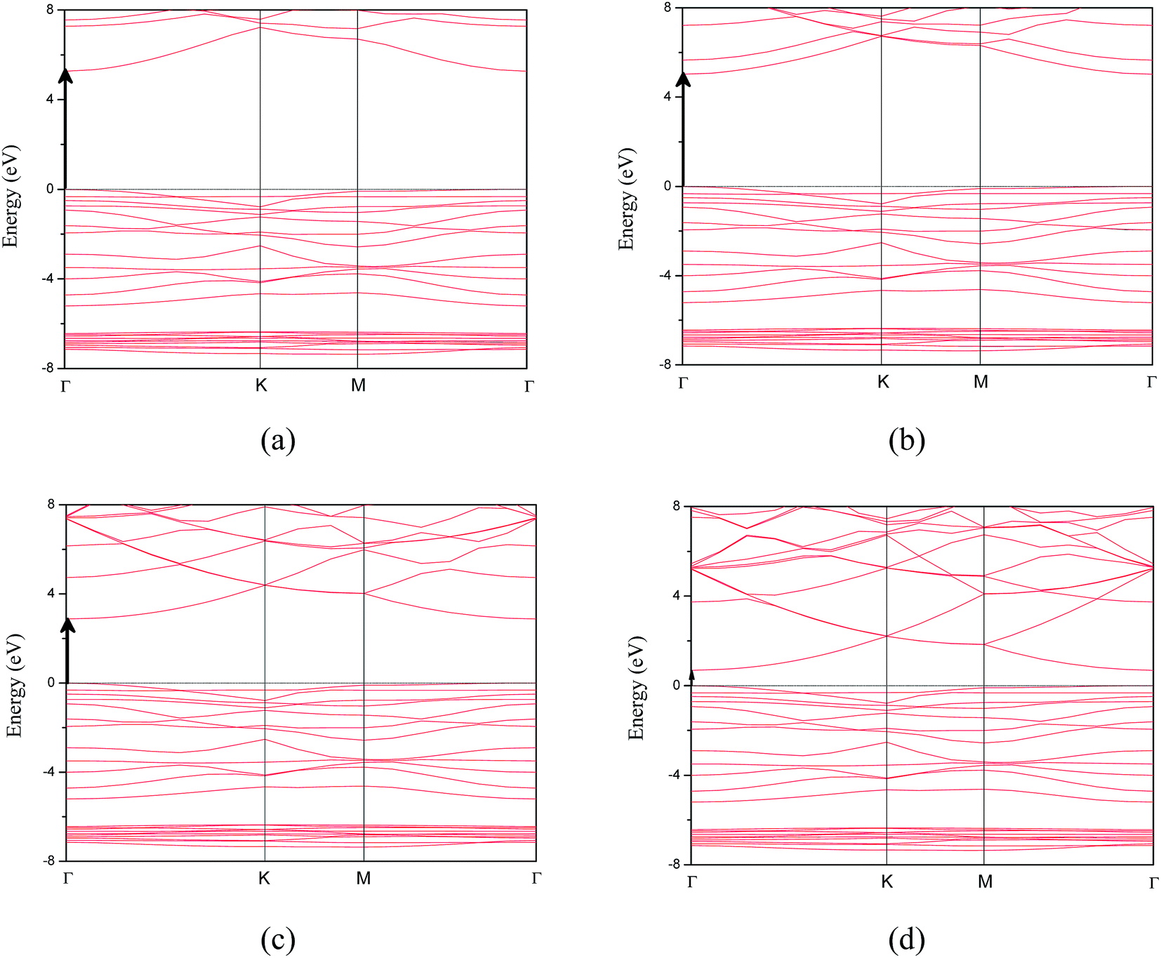 | ||
| Fig. 4 The band structures of MgZnO monolayer under electric field of (a) 0.0 V Å−1, (b) 0.5 V Å−1, (c) 1.0 V Å−1 and (d) 1.4 V Å−1. | ||
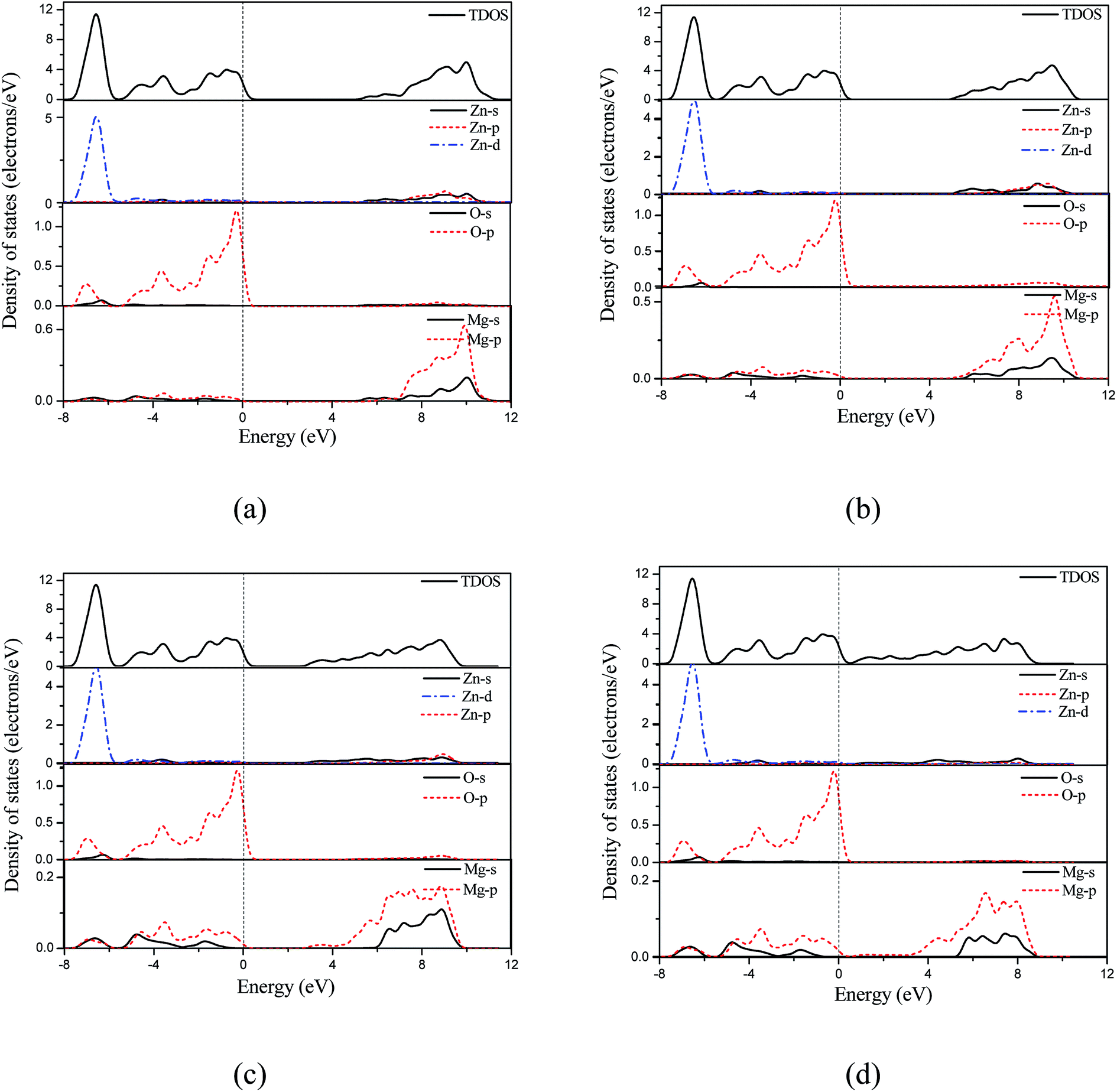 | ||
| Fig. 5 The density of states of MgZnO monolayer under electric field of (a) 0.0 V Å−1, (b) 0.5 V Å−1, (c) 1.0 V Å−1 and (d) 1.4 V Å−1. | ||
3.2 Optical properties of MgZnO monolayer
In general, the optical properties of semiconductors are closely related to their electronic structures and are of great importance to their application. Thus, we calculated and discussed the optical properties of MgZnO monolayer under electric field. The imaginary part ε2(w) of the dielectric function has been obtained from the electronic structure calculations, using the following expression:31
 | (2) |
In this expression, M is the dipole matrix, i and j are the initial and final states, respectively, fi is the Fermi distribution as a function of the ith state, and Ei is the energy of electron in the ith state.
The real part of dielectric function ε1(w) can be extracted using the Kramers–Krong relation:32
 | (3) |
Indeed, these two parts allow us to determine other properties, such as absorption coefficient α(ω) and the reflectance R(ω) using the following relations:33
 | (4) |
 | (5) |
To examine the effect of the MgZnO on the optical properties, we also investigated the optical properties of MgZnO monolayer with electric fields of 0.0, 0.5, 1.0 and 1.4. It is well known that the complex dielectric function of a material reflects the information between the energy band structure and optical transition. We first investigated the imaginary part of the dielectric function, which is plotted in Fig. 6. It is clear that there are three main peaks in MgZnO monolayer without electric field effect. The first peak at 5.90 eV should primarily be caused by the optical transition between the O 2p states in the highest valence band and the Zn-4s states in the lowest valance band. The second and third peaks are located at 9.46 and 12.89 eV, respectively. The main effect may be due to the transition of Zn 3d, O 2p and O2s states. On increasing the external electric field, the secondary peaks in the high energy red-shift to a lower energy side. This mechanism can be useful for the design and optimization of field-effect optoelectronic devices. In particular, Fig. 6 shows a new peak in the low energy (about 5 eV) under 1.0 electric field. On increasing the electric field, the new peak shifts to the lower energy side.
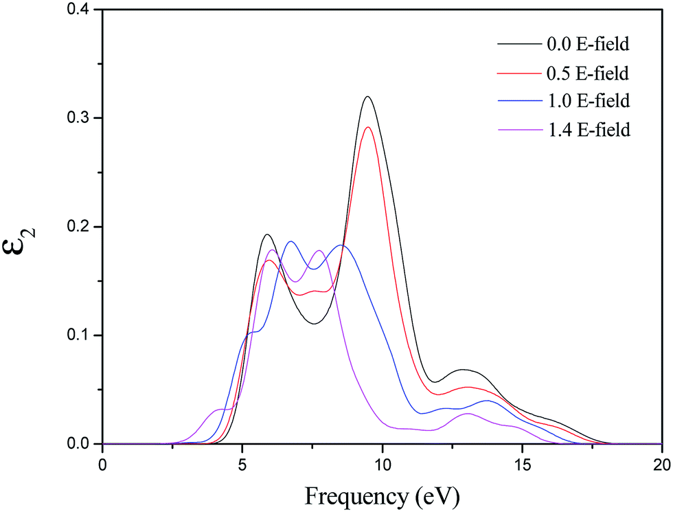 | ||
| Fig. 6 The variation with electric field of imaginary part of dielectric function of MgZnO monolayer. | ||
We also calculated the absorption coefficients and reflectivity of MgZnO monolayer by applying the external electrical field as shown in Fig. 7. For the absorption coefficients, the changes of line shapes, energy positions and strengths of the peaks are similar to those of imaginary part of the dielectric function. Furthermore, as shown in Fig. 7(b), the reflectivity decreases with increasing external electric field of MgZnO monolayer. Based on the above analysis, the application of external electric field is an effective method for MgZnO materials as ultraviolet optoelectronic devices.
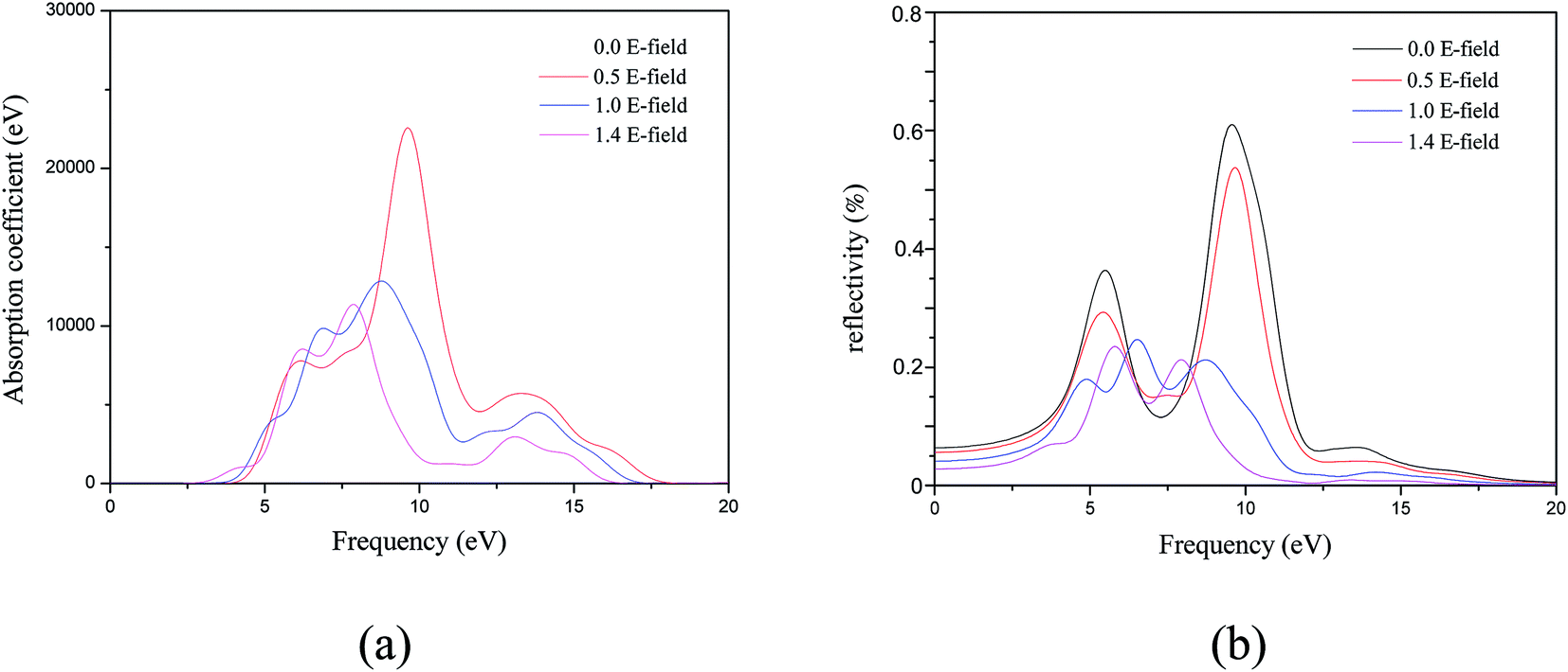 | ||
| Fig. 7 The variation with electric field of (a) absorption coefficient and (b) reflectivity of MgZnO monolayer. | ||
4. Conclusions
In summary, the external electric field inducing tenability of the electronic band structure in MgZnO monolayer has been comprehensively addressed using first-principles density functional theory in our study. The band gap of MgZnO monolayer shows a decrease with an increase in external electric field and can be tuned from 5.27 eV to 0.69 eV by increasing the external electric field. Moreover, we also found a red shift of the optical absorption peaks with increase in electric field. Furthermore, the absorption coefficients and reflectivity decreases on increasing external electric field over the MgZnO monolayer. Our findings suggest that the realization of ultrawide range tuning of band gap opens up exciting opportunities for the development of electronic optoelectronic devices based on MgZnO monolayer system.Author contributions
Changlong Tan conceived and designed the experiments; Changlong Tan, Dan Sun, Hongfei Chen performed the experiments; Changlong Tan, Dan Sun, Hongfei Chen, Xiaohua Tian analyzed the data; Changlong Tan, Dan Sun, Hongfei Chen, Xiaohua Tian and Yuewu Huang wrote the paper.Conflicts of interest
The authors declare no conflict of interestAcknowledgements
The authors acknowledge the supports of National Natural Science Foundation of China (Grant No. 51471064 and 51301054); the Program for New Century Excellent Talents (Grant No. 1253-NCET-009) and Program for Youth Academic Backbone in Heilongjiang Provincial University (Grant No. 1251G022).References
- P. Avouris, Nano Lett., 2010, 10, 4285–4294 CrossRef CAS PubMed.
- J. M. Marmolejo-Tejada and J. Velasco-Medina, Microelectron. J., 2016, 48, 18–38 CrossRef CAS.
- F. Schwierz, Nat. Nanotechnol., 2010, 5, 487–496 CrossRef CAS PubMed.
- Ü. Özgür, Y. I. Alivov, C. Liu, A. Teke, M. Reshchikov, S. Doğan, V. Avrutin, S.-J. Cho and H. Morkoc, J. Appl. Phys., 2005, 98, 11 CrossRef.
- Z. L. Wang, J. Phys.: Condens. Matter, 2004, 16, R829 CrossRef CAS.
- S. J. Pearton, D. P. Norton, K. Ip, Y. W. Heo and T. Steiner, Prog. Mater. Sci., 2005, 50, 293–340 CrossRef CAS.
- A. Tsukazaki, A. Ohtomo, T. Onuma, M. Ohtani, T. Makino, M. Sumiya, K. Ohtani, S. F. Chichibu, S. Fuke, Y. Segawa, H. Ohno, H. Koinuma and M. Kawasaki, Nat. Mater., 2005, 4, 42 CrossRef CAS.
- S. Chu, J. H. Lim, L. J. Mandalapu, Z. Yang, L. Li and J. L. Liu, Appl. Phys. Lett., 2008, 92, 152103 CrossRef.
- J. Huang, Z. Yin and Q. Zheng, Energy Environ. Sci., 2011, 4, 3861–3877 CAS.
- K. P. Shinde, R. C. Pawar, B. B. Sinha, H. S. Kim, S. S. Oh and K. C. Chung, J. Alloys Compd., 2014, 617, 404–407 CrossRef CAS.
- M. P. Lu, M. Y. Lu and L. J. Chen, Nano Energy, 2012, 1, 247–258 CrossRef CAS.
- K. S. Novoselov, A. K. Geim, S. V. Morozov, D. Jiang, Y. Zhang, S. V. Dubonos, I. V. Grigorieva and A. A. Firsov, Science, 2004, 306, 666–669 CrossRef CAS PubMed.
- Q. Tang and Z. Zhou, Prog. Mater. Sci., 2013, 58, 1244–1315 CrossRef CAS.
- K. J. Koski and Y. Cui, ACS Nano, 2013, 7, 3739–3743 CrossRef CAS PubMed.
- X. Song, J. Hu and H. Zeng, J. Mater. Chem. C, 2013, 1, 2952–2969 RSC.
- S. Z. Butler, S. M. Hollen and L. Y. Cao, ACS Nano, 2013, 7, 2898–2926 CrossRef CAS PubMed.
- C. L. Tan, D. Sun, X. H. Tian and Y. W. Huang, Materials, 2016, 9, 877 CrossRef PubMed.
- W. Wu, P. Lu, Z. Zhang and W. Guo, ACS Appl. Mater. Interfaces, 2011, 3, 4787–4795 CAS.
- C. Zhang, A. D. Sarkar and R.-Q. Zhang, J. Phys. Chem. C, 2011, 115, pp23682–23687 Search PubMed.
- N. D. Drummond, V. Zólyomi and V. I. Fal'ko, Phys. Rev. B: Condens. Matter Mater. Phys., 2012, 85, 075423 CrossRef.
- Z. Y. Ni, Q. H. Liu, K. C. Tang, J. X. Zheng, J. Zhou, R. Qin, Z. X. Gao, D. P. Yu and J. Lu, Nano Lett., 2012, 12, 113–118 CrossRef CAS PubMed.
- L. Li, E. C. O. Farrell, K. P. Loh, G. Eda, B. Ozyilmaz and A. C. Neto, Nature, 2015, 529, 185 CrossRef PubMed.
- Y. Zheng, T. Zhou, X. Zhao, W. K. Pang, H. Gao, S. Li, Z. Zhou, H. Liu and Z. Guo, Adv. Mater., 2017, 29, 1700396 CrossRef PubMed.
- M. D. Segall, P. J. D. Lindan, M. J. Probert, C. J. Pickard, P. J. Hassnip, S. J. Clark and M. D. Payne, J. Phys.: Condens. Matter, 1990, 14, 7892–7895 Search PubMed.
- D. Vanderbilt, Phys. Rev. B: Condens. Matter Mater. Phys., 1990, 41, 7892–7895 CrossRef.
- H. J. Monkhorst and J. D. Pack, Phys. Rev. B: Condens. Matter Mater. Phys., 1976, 13, 5188–5192 CrossRef.
- C. L. Tan, D. Sun, X. H. Tian and Y. W. Huang, Ceram. Int., 2016, 42, 10997–11002 CrossRef CAS.
- U. Ozgur, Y. I. Alivov, C. Liu, A. Teke, M. A. Reshchikov, S. Dogan, V. Avrutin, S. J. Cho and H. Morkoc, J. Appl. Phys., 2005, 98, 041301 CrossRef.
- A. Splendiani, L. Sun, Y. Zhang, T. Li, J. Kim, C. Y. Chim, G. Galli and F. Wang, Nano Lett., 2010, 10, 1271–1275 CrossRef CAS PubMed.
- K. F. Mak, C. Lee, J. Hone, J. Shan and T. F. Heinz, Phys. Rev. Lett., 2010, 105, 136805 CrossRef PubMed.
- C. M. I. Okoye, J. Phys.: Condens. Matter, 2003, 15, 5945 CrossRef CAS.
- B. Amin, I. Ahmad, M. Maqbool, S. Goumri-Said and R. Ahmad, J. Appl. Phys., 2011, 109, 023109 CrossRef.
- J. Sun, H. T. Wang, J. He and Y. Tian, Phys. Rev. B: Condens. Matter Mater. Phys., 2005, 71, 125132 CrossRef.
| This journal is © The Royal Society of Chemistry 2018 |