
 Open Access Article
 This Open Access Article is licensed under a Creative Commons Attribution-Non Commercial 3.0 Unported Licence
Single step electrodeposition process using ionic liquid to grow highly luminescent silicon/rare earth (Er, Tb) thin films with tunable composition
Shibin Thomasa,
Jeremy Mallet*a,
Hervé Rinnertb and
Michael Molinari *a
*a
aLaboratoire de Recherche en Nanosciences, LRN EA4682, Université de Reims Champagne-Ardenne, Campus Moulin de la Housse, BP 1039, 51687 Reims, France. E-mail: michael.molinari@univ-reims.fr; jeremy.mallet@univ-reims.fr
bUniversité de Lorraine, Institut Jean Lamour UMR CNRS 7198, 54506 Vandœuvre-lès-Nancy Cedex, B.P. 70239, France
First published on 19th January 2018
Abstract
A one-step method for the electrodeposition of silicon–erbium (Si/Er) and silicon–terbium (Si/Tb) thin films using room temperature ionic liquid (RTIL) has been successfully developed. By playing with the electrochemical parameters, the concentration of incorporated rare earth (RE) ions (Er3+ and Tb3+) in the thin films can be tuned. The obtained thin films have been characterized by electron microscopy and composition analysis techniques. The structural quality of the obtained thin films is characterized by a uniform distribution of Si atoms and RE ions throughout the thickness. The study of the optical properties, carried out by photoluminescence (PL) spectroscopy, demonstrates the efficient optical activity of the films with typical Er and Tb luminescence at room temperature depending on the RE content. The deposition method described is a promising strategy for incorporating RE ions in semiconducting thin films to achieve materials for opto-electronic applications.
1. Introduction
Rare earth doped semiconductors are intensively studied due to their unique electronic and optical properties.1,2 RE ions are characterized by their narrow and efficient emission lines in the visible and near infrared (NIR) range which are almost insensitive to their host matrices due to the shielding effect of outer 5s and 5p electrons. Among the RE ions, Er3+ has gained more attention because of its highly efficient light emission at 1.53 μm.3 Similarly, Tb3+ has strong radiative intra 4f transitions in the visible wavelengths close to the typical blue-green colour.4 So, materials incorporating these ions are considered as potential candidates in modern opto-electronics. As silicon is currently the most leading functional material for industrial applications, RE incorporation in Si represents a promising way of developing silicon based opto-electronics. RE incorporated Si materials are widely used for applications in telecommunication,5 photovoltaics6,7 and display applications such as electroluminescence8,9 or Light Emitting Diodes (LEDs).10A great number of techniques have been developed to incorporate the RE ions into silicon, such as ion implantation,11 magnetron co-sputtering12,13 and plasma enhanced chemical vapour deposition (PECVD).14,15 However these current synthesis methods involve constraining deposition conditions such as high vacuum, high temperature, different steps of growth and the use of potentially dangerous precursors which makes these processes complicated and expensive. Therefore, the development of low cost and non-constraining alternative techniques for the RE incorporation in Si is of primary importance.
Electrochemical growth methods have emerged as low cost techniques as it operates low temperatures and does not involve any high vacuum or other constraining conditions. Electrodeposition of metals and semiconductor compounds from aqueous electrolytes has been extensively studied by various researchers and it is currently a well-established field. However, elemental Si and RE metals cannot be electrodeposited from aqueous electrolytes due to their large reduction potential and also to the high reactivity of the common precursors such as Si or RE halides with water. Besides, the RE metals are highly corrosive in aqueous medium as they react with water to give hydrogen and metal hydroxides or oxides.16 Hence, the electrodeposition of Si and RE metals requires the use of a non-aqueous electrolytic medium such as RTILs,17–19 organic solvents20–22 or molten salts.23–25 Among these solvents, the RTILs offer a number of advantages such as wide electrochemical window, high ionic conductivity, superior thermal stability and negligible vapour pressure.26 In addition to being less corrosive than other non-aqueous electrolytes, RTILs allow deposition at relatively lower temperatures. Additionally, they offer high solubility to most of the semiconductor and reactive metal salts, including the salts of rare earth metals, facilitating their use as the solvent for electrodeposition.
There have been a number of reports on the electrodeposition of elemental Si or its alloys from RTILs.27–32 However, the use of RTILs for the deposition of RE metals is not well attended and there have been only very few attempts towards the realization of it.33,34 A comparison of the Er3+ electroreduction from different non-aqueous electrolytes including quaternary ammonium based ionic liquids has been reported recently by Small et al.,35 however, obtaining RE deposits with high purity remains challenging. To our knowledge, there are no other reports on the use of RTILs for the electrodeposition of Er and Tb, which are highly important dopants in Si based opto-electronic materials. These two RE metal ions differs in their optical emission properties, Er3+ emitting in the Near Infra-Red (NIR) and Tb3+ emitting in the visible range of the electromagnetic spectrum which enables to cover a large field of applications. Electrochemical incorporation of RE ions in silicon has been demonstrated in the literature,36–39 however, the technique is only limited to the porous Si (p-Si) systems which is a fragile material and suffers from instability issues to consider for opto-electronic applications. Additionally, the technique is a two-step approach where the p-Si is fabricated by anodic etching process in the first step followed by the incorporation of RE ions by electrochemical polarisation. The involvement of multi-step fabrication routes and the requirement of potentially dangerous chemicals such as HF makes the process complex and inappropriate for large scale production.
The present study demonstrates the successful electrodeposition of metallic Er and Tb with high purity from RTIL for the first time, and develops a novel electrochemical approach for obtaining Si/RE thin films by co-depositing RE metals with Si. Besides, it is shown that the RE content in Si thin films can be tuned by controlling the electrochemical parameters. Finally, the luminescence properties of the deposited Si/RE thin films have been investigated to confirm the potential of the materials for applications in modern opto-electronics.
2. Experimental
For the present study, 1-butyl-1-methylpyrrolidinium bis(trifluoromethylsulfonyl)imide ([Py1,4]TFSI) ionic liquid purchased from Solvionic was used as the solvent for electrodeposition of RE metals and Si. The quality of [Py1,4]TFSI given by the supplier is 99.99%. In order to reduce the water content, the IL was dried under vacuum at 100 °C for at least 5 days. The drying of the IL was performed in an argon filled glove box (Innovative Technology) with oxygen and moisture content below 1 ppm. Silicon tetrachloride (99.998%), erbium chloride (99.99%) and terbium chloride (99.99%) purchased from Sigma Aldrich were used as the precursors for silicon, erbium and terbium respectively.All the electrochemical studies were performed inside an Argon filled glove box using a three electrode based electrochemical cell. n-Doped silicon (100) substrate was used as the working electrode for the deposition. Prior to use, the Si substrates were treated with ammonium fluoride–hydrofluoric acid mixture etching solution to remove the natural oxide (SiOx) layer on the surface. Platinum wire was used as the quasi-reference electrode which provides relatively stable electrode potentials for the present electrochemical studies. A platinum wire was used as the counter electrode. Utmost care was given for the cleaning and drying of the electrochemical cell and the electrodes before performing the electrochemical experiments. All the electrochemical measurements were done using a Voltalab PGZ 100 potentiostat/galvanostat controlled by Voltamaster 4 software. The experiments were carried out at a controlled temperature of 70 °C which enables to limit possible heating effects during the process and thus enhances its reproducibility. The surface morphology of the deposited thin film was obtained by a Scanning Electron Microscopy (SEM, HITACHI S-3400N). The chemical composition of the deposit was analysed by Energy Dispersive X-ray spectroscopy (EDX) coupled to the SEM. The composition and homogeneity of the thin films were further analysed by Secondary Ion Mass Spectrometry (SIMS). The photoluminescence (PL) spectra were obtained using the 325 nm line of a He–Cd laser for the excitation and the sample emission was collected with a monochromator equipped with an InGaAs photomultiplier cooled at 140 K.
3. Results and discussion
3.1. Electrodeposition of Si
In order to study the electrochemical stability of the RTIL and to understand the electrochemical processes at the interface, Cyclic Voltammetry (CV) was performed. Fig. 1a shows the CV's of pure [Py1,4]TFSI (dashed line) and 0.01 M SiCl4 in [Py1,4]TFSI (solid line) recorded on Si (100) substrate at a scan rate of 10 mV s−1. The CV of pure [Py1,4]TFSI does not show any cathodic reduction peaks till −3.5 V, which indicates the stability of the IL in the cathodic scan. The rise of current below −3.5 V could be attributed to the breakdown of the organic cation, i.e. the cathodic reduction of [Py1,4]+ cation. The CV of the [Py1,4]TFSI confirms that the IL is pure, dry and electrochemically stable enough to be used as the solvent for electrodeposition. The electrochemical window of [Py1,4]TFSI is calculated to be around 5 V. The high electrochemical stability of the IL, especially in the cathodic regime, makes possible the electrodeposition of semiconductors and RE metals. As can be seen in the Fig. 1a, the CV of 0.01 M SiCl4 in [Py1,4]TFSI exhibits two reduction peaks, observed at −1 V and −2.5 V in the cathodic scan. The origin of the reduction peak at −1 V is not yet fully understood, however it could be related to some charging/discharging process occurring at the interface. In order to confirm that this reduction peak is not related to the electro reduction of Si, electrodeposition has been done by applying potentials between −1 V and −2 V. No observable deposits have been obtained on the substrate. The reduction peak at −2.5 V is due to the bulk reduction of silicon onto the working electrode, which is confirmed by the EDX analysis of the yellowish white film obtained on the substrate.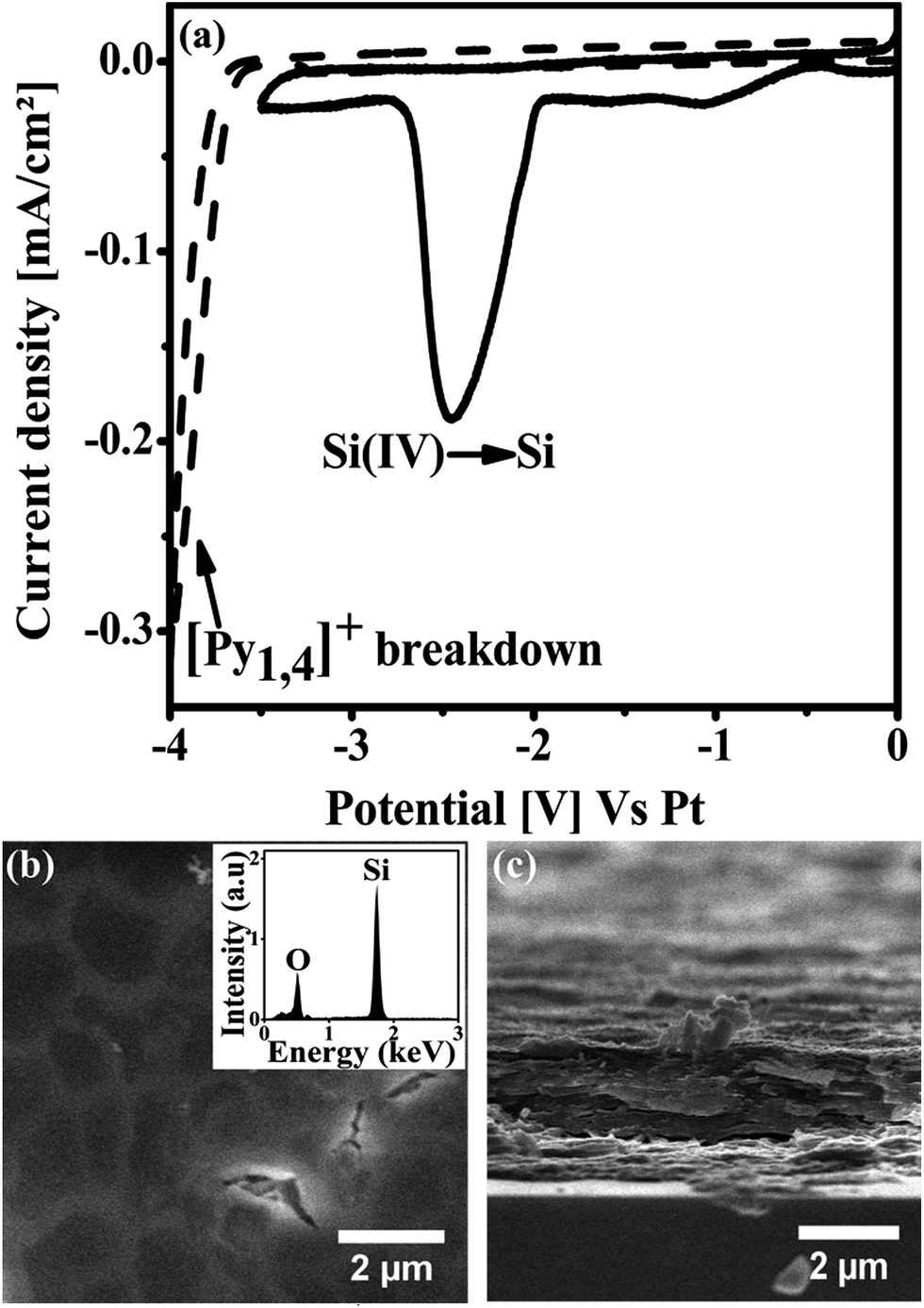 | ||
| Fig. 1 (a) CV (scan rate of 10 mV s−1) of pure [Py1,4]TFSI (dashed line) and [Py1,4]TFSI with 0.01 M SiCl4 (solid line) on Si (100) substrate vs. Pt at 70 °C. (b) Top view SEM image of the Si thin film obtained by potentiostatic deposition at −2.7 V vs. Pt. Inset shows the EDX profile of the Si deposit. (c) Cross-section SEM image of the Si thin film. | ||
Fig. 1b shows the top view SEM image of the Si deposit obtained by applying a constant potential of −2.7 V for 1 hour at 70 °C. The deposition leads to the formation of a homogeneous Si thin film on the electrode. The morphology of the deposit reveals the roughness of the film containing few cracks on the surface. These cracks observed at high magnification (Fig. 1b) could be a result of internal stresses during the deposition. EDX analysis (inset of Fig. 1b) performed simultaneously with SEM imaging shows that the thin film consists of only Si and O. No other impurities were detected in the detection limit of the EDX spectroscopy. The presence of oxygen is due to the oxidation of Si in air during the storage of deposit prior to the SEM and EDX observation. Fig. 1c shows the cross-section SEM image of the Si thin film. It is clear from the image that the thin film growth occurs in a laminar fashion resulting in a dense compact film at the end. The thickness of the deposit is measured to be 1.6 μm. Careful examinations of the SEM images, supported by the similarities of the present growth conditions with previous reports,27,28,40 suggest that the deposited Si is amorphous in nature. The above results shows that pure a-Si thin film was electrodeposited from [Py1,4]TFSI, which is an important preliminary step for the further studies described in this article.
3.2. Electrodeposition of RE (Er, Tb) metals
Prior to perform the co-deposition of RE metals with Si, the possibility of electrodeposition of pure RE metals from RTIL has been studied. The results described below shows the successful electrodeposition of pure Er and Tb metals from RTIL.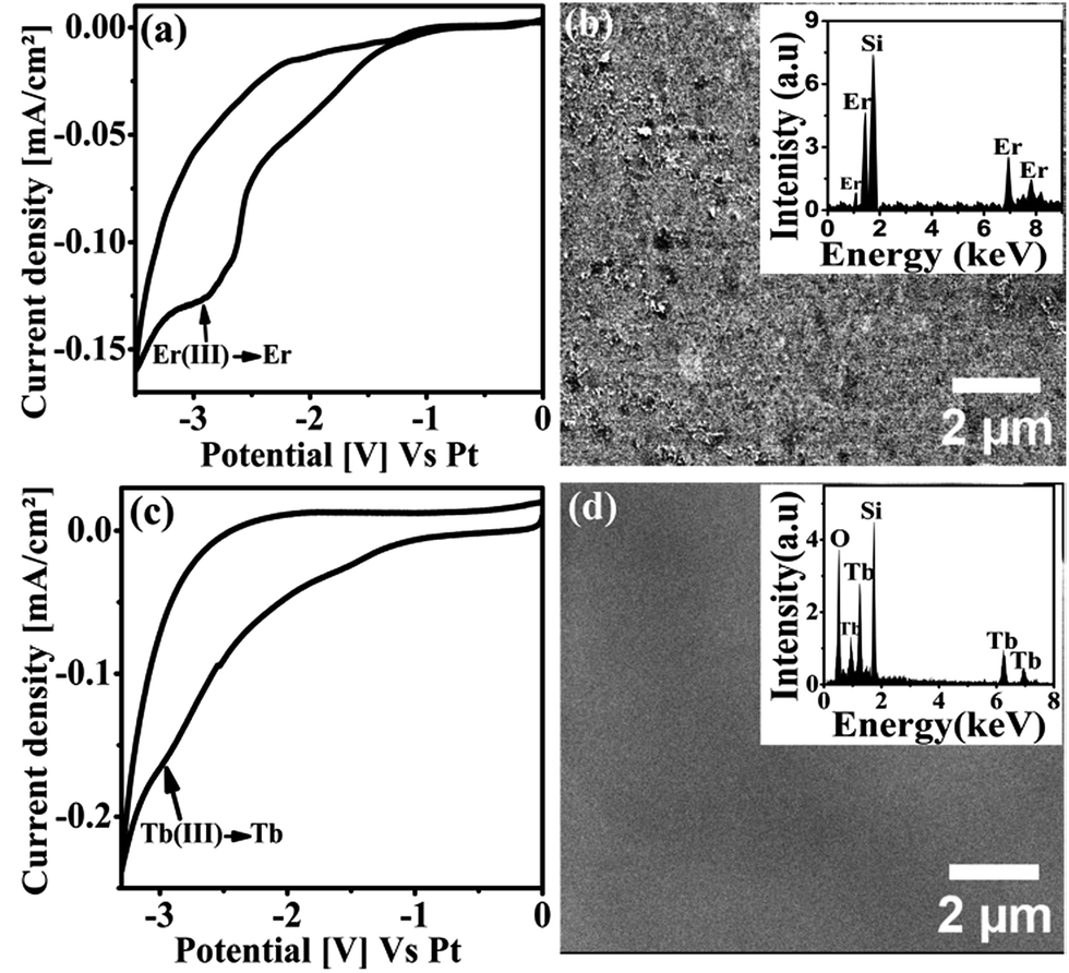 | ||
| Fig. 2 (a) CV (scan rate of 10 mV s−1) of [Py1,4]TFSI with 0.01 M ErCl3 on Si (100) substrate vs. Pt at 70 °C. (b) Top view SEM image of the Er thin film deposited by applying −3.2 V vs. Pt. Inset shows the corresponding EDX spectrum (c) CV (scan rate of 10 mV s−1) of [Py1,4]TFSI with 0.01 M TbCl3 on Si (100) substrate vs. Pt at 70 °C. (d) Top view SEM image of Tb thin film deposited by applying −3.2 V vs. Pt. Inset shows the EDX spectrum obtained from the deposit. | ||
After identifying the reduction potential of Er from the CV, potentiostatic electrodeposition was performed by applying −3.2 V for 1 hour onto Si (100) substrate using 0.01 M ErCl3 in [Py1,4]TFSI at 70 °C. The surface morphology of the obtained deposit was characterized by the SEM. Fig. 2b shows the representative top view SEM image obtained from the metallic Er thin film. It can be observed from the image that the potentiostatic deposition leads to a homogeneous deposition of Er on the substrate. The surface of the metallic thin film is rough and contains few micrometre sized clusters. The chemical composition of the thin film was analysed by EDX (Fig. 2b inset) which gave signals of mainly Er with no significant impurities or oxygen in the detection limit, meaning that the deposited thin film comprises of pure Er metal. The Si signal observed in the EDX spectrum is due to the Si (100) substrate used for deposition.
Metallic Tb was potentiostatically electrodeposited onto Si (100) substrate from 0.01 M TbCl3 in [Py1,4]TFSI by applying −3.2 V for 1 hour at 70 °C. Fig. 2d shows the top view SEM image of the deposited Tb thin film. The thin film evolves as a smooth homogeneous layer on the substrate. The EDX analysis (Fig. 2d inset) reveals the presence of Tb and O in the thin film. Metallic Tb is well known for its affinity towards oxygen.41 The Tb deposit undergoes oxidation in air to form its oxides (Tb1−xOx) as it is exposed to the ambient atmosphere. The Si signal is arising from the Si (100) substrate used. The result shows that pure Tb thin film is successfully electrodeposited from the RTIL, which turns into Tb1−xOx once exposed to the air.
3.3. Co-deposition of RE (Er, Tb) metals with Si
Understanding the potential for RTILs in electrodepositing both Si and RE (Er, Tb) metals is mandatory to study the possibility of co-depositing Si with RE metals, as the principle of the co-deposition is to use the two precursors (Si and RE) in the solution and to work at a given potential appropriate for the deposition of the two metals. The results of the investigation are described below.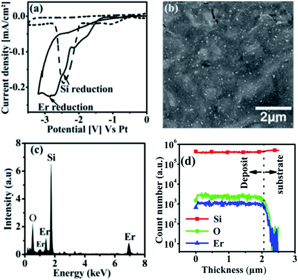 | ||
| Fig. 3 (a) CV (scan rate of 10 mV s−1) of [Py1,4]TFSI with 0.01 M SiCl4 and 0.01 M ErCl3 (solid line) on Si (100) substrate vs. Pt at 70 °C. The dashed line represents the CV of [Py1,4]TFSI with 0.01 M SiCl4 alone. (b) Top view SEM image of the Si/Er thin film obtained by applying −3.2 V vs. Pt. (c) The EDX spectrum obtained from the Si/Er thin film. (d) SIMS depth profile of the deposit. | ||
The CV was used to determine the potential range for performing the co-deposition of Si with Er. The co-deposition of Si/Er thin film was done potentiostatically by applying −3.2 V for 1 hour at 70 °C. Fig. 3b shows the top view SEM image of the deposited Si/Er thin film. It can be seen clearly from the image that the deposit comprises of a thin film homogeneously covering the substrate with some roughness observed on the surface. The deposit grows uniformly in the beginning of the deposition to make a smooth thin film covering the electrode. As the deposition progresses, the higher electrical resistance of the deposited Si/Er layer and the internal stresses formed at the surface cause non-uniform distribution of the particles, leading to the formation of micro islands and small cracks on the surface. X-ray diffraction experiments (not shown here) shown that the deposited thin film is amorphous in nature. In order to confirm the presence of Er in the Si thin film, EDX analysis was performed on the deposit. Fig. 3c shows the EDX spectrum for the Si/Er deposit. The spectrum shows the signals corresponding to Si, O and Er which indicates clearly the successful incorporation of Er in the Si thin film. The presence of oxygen is due to the unavoidable oxidation of Si in the atmosphere. An estimation of the elemental composition of the thin films using EDX shows that the content of Er in the thin film varies between 8–13 atomic percentages (at%). In order to gain insights on the homogeneity of the thin film along the thickness, SIMS depth profile analysis has been performed on the deposit. Fig. 3d shows the SIMS depth profile of the Si/Er thin film. The depth profile reveals the signals of Si, Er and O. As can be seen from the spectrum, the thin film has uniform composition throughout the depth, demonstrated by the uniform ionic yields of Si, Er and O starting from the uppermost surface till the substrate interface.
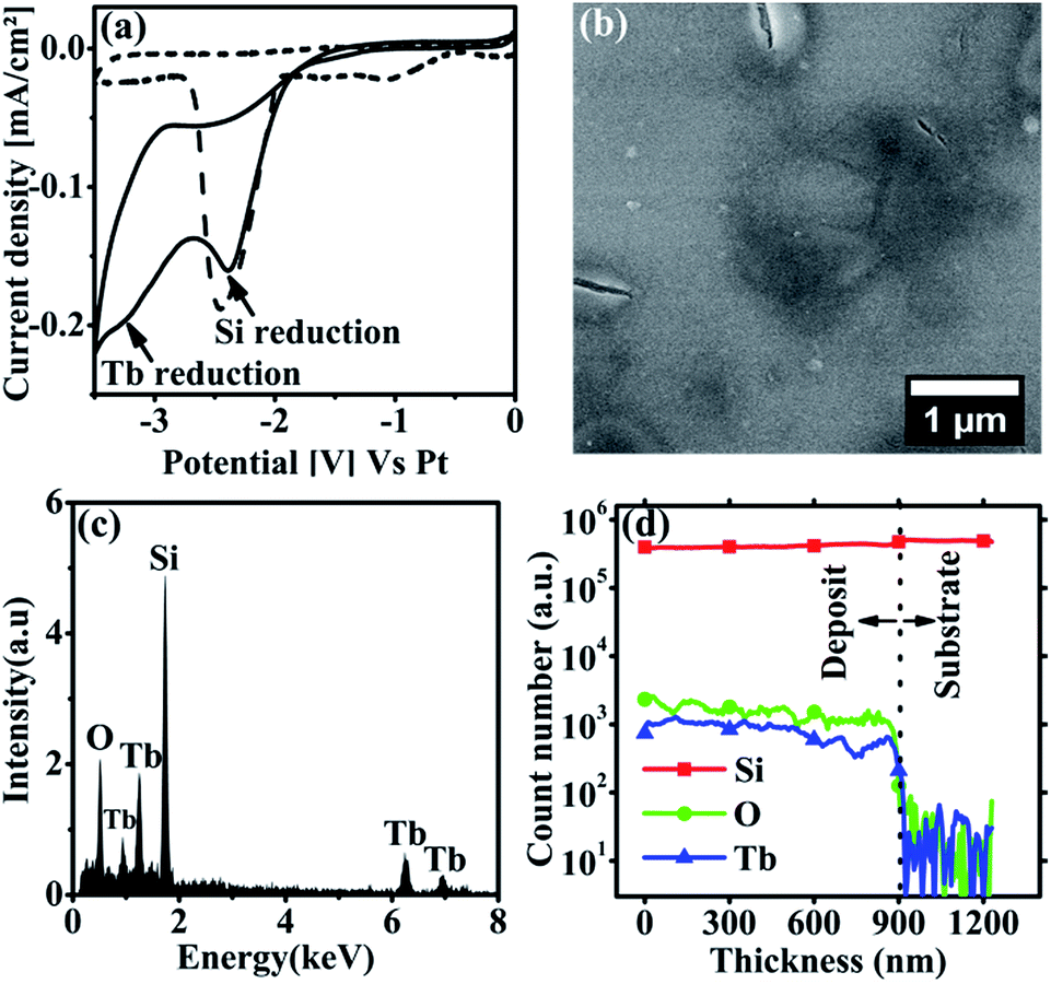 | ||
| Fig. 4 (a) CV (scan rate of 10 mV s−1) of [Py1,4]TFSI with 0.01 M SiCl4 and 0.01 M TbCl3 (solid line) on Si (100) substrate vs. Pt. at 70 °C. The dashed line represents the CV of [Py1,4]TFSI with 0.01 M SiCl4 alone. (b) Top view SEM image of the Si/Tb thin film obtained by applying −3.2 V vs. Pt. (c) The EDX spectrum obtained from the Si/Tb thin film. (d) SIMS depth profile of the deposit. | ||
The co-deposition of Si/Tb thin film was done potentiostatically onto Si (100) substrate by applying −3.2 V for 1 hour at 70 °C. Fig. 4b shows the top view SEM image of the obtained Si/Tb thin film. Contrary to the Si/Er thin film, the morphology of Si/Tb thin film shows a flat and smooth deposit with few small cracks on the surface. It is worth comparing this with the SEM images of the pure RE metal deposits (Fig. 2b and d) where the metallic Er thin film was observed to be rougher while the Tb thin film was very flat and smooth. It suggests that the nature of the RE metal can possibly influence the surface morphology of the deposit. Fig. 4c shows the EDX spectrum obtained from the Si/Tb thin film. The spectrum gives the signatures for Si, Tb and O, indicating the successful incorporation of Tb in the Si thin film. Both Si and Tb contribute to the oxide content in the deposit as both the elements have strong affinity towards oxygen.
To confirm the homogeneity of the Tb incorporation in the thin film, SIMS depth profile analysis was performed. Fig. 4d shows the depth profile of the Si/Tb thin film. As evident from the spectrum, a quite uniform distribution of Tb and Si throughout the thickness of the deposit is observed. Additionally, the oxygen, which is bound to the Si and Tb here, is also found to be uniformly distributed along the thickness of the film. The SIMS depth profile confirms that the homogeneity and uniform chemical composition of the thin film are maintained throughout the growth.
3.4. Concentration of RE (Er, Tb) in Si thin films-tunability
For the optical applications of the thin films, it is important to control the concentration of RE ions in the Si thin film. So, the possibility of controlling the RE concentration in the thin films by adjusting the electrochemical parameters has been studied.Fig. 5 shows a schematic representation of a voltammogram showing the potential regimes to deposit different elements comprising the thin film. As can be seen in the figure, the voltammogram is divided into three potential regions. Region A (−1 to −1.8 V) represents the cathodic potential range in which no observable deposit is obtained by electrodeposition. Neither Si nor RE metals can be deposited at this potential range. Region B (−1.8 V to −2.6 V) represents the cathodic potentials in which pure Si is being electrodeposited and no significant contribution from the RE metal ions is detected. Region C (−2.7 V to −3.5 V) in the voltammogram represents the potential range in which a co-deposition of Si and RE metals occurs, resulting in the Si/RE thin films.
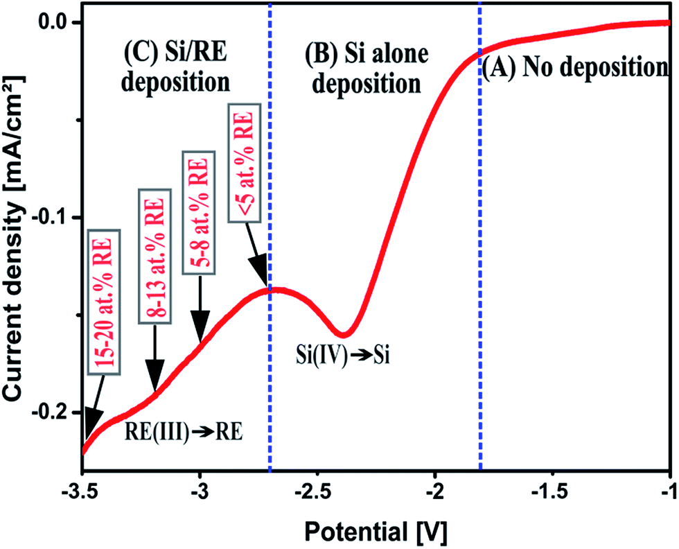 | ||
| Fig. 5 Schematic representation of the cathodic potential regions for electrodeposition of pure Si and RE (Er, Tb) incorporated Si thin films. | ||
Region C in Fig. 5 is of great importance as it gives the range of potentials in which RE metals are being co-deposited with Si. Herein it is shown that it is possible to easily control the RE ion content in the Si thin film by varying a single electrochemical parameter: the applied potential. Electrochemical co-deposition of Si and RE (Er and Tb) was performed by applying different potentials in the range from −2.7 V to −3.5 V.
The deposited thin films were analysed by EDX to check the composition of the deposits and for the estimation of the RE content in the thin films. Table 1 shows the dependence of RE content in the deposits with the applied potential. An applied potential of −2.7 V resulted in Si thin films with very low (<5 at%) RE content while the application of −3.5 V gave deposits containing 15–20 at% of RE. It is clear from Table 1 that the decrease of the applied potential leads to an increase of RE content in the thin films. It is important to point out here that the deposits obtained by applying −3.5 V shows the inclusion of some impurities such as sulfur and carbon, which is due to the decomposition of the IL at higher negative potentials. However a thorough cleaning of the deposits by immersing it in ethanol for prolonged period resulted in decreasing the impurity levels to negligible values, meaning that the impurities are rather a surface contamination than being incorporated in the thin film. The above results show that the electrodeposition in RTILs offers not only a single step process for the incorporation of RE ions in Si, but also provides an easy way to control the concentration of RE ions in the thin films.
| Applied potential (V vs. Pt) | Atomic% of RE (Tb, Er) in deposit |
|---|---|
| −2.7 V | <5% |
| −3 V | 5–8% |
| −3.2 V | 8–13% |
| −3.5 V | 15–20% |
3.5. Optical properties
For applications of the thin films in silicon-based light emitting systems, PL measurements were carried out on both Si/Er and Si/Tb thin films. The Si/Er thin film obtained by applying −3 V, having approximately 8 at% of Er, was chosen for the initial PL experiments. The PL measurements were done with an excitation at 325 nm. The black solid line in Fig. 6a shows the PL emission spectrum obtained from Si/Er thin film at room temperature (RT). As evident from the spectrum, the PL gave a weak emission at 1530 nm, which is characteristic of the 4I15/2–4I13/2 intra 4f transition in Er3+ ions in Si. The peak shoulder observed at 1545 nm is due to the stark splitting of the Er3+ energy levels resulting in the peak splitting of the luminescence band.42 In order to obtain an efficient PL emission, the Er incorporated Si materials has to be annealed under oxygen atmosphere, which is an important step to optically activate the Er3+ ions in the Si matrix.43–45 Therefore the Si/Er thin film was annealed at 650 °C under oxygen for 5 minutes. The red solid line in Fig. 6a shows the PL spectrum obtained at RT from the annealed Si/Er thin film. The PL gave a strong emission band at 1530 nm which is highly intense compared to the PL obtained from the non-annealed deposit. The high temperature annealing process enhances the oxygen diffusion into the Si/Er thin film and leads to the formation of Er–O complexes,46 which act as efficient electronic traps. In addition, the complexation of Er with oxygen produces a solvation shell around the Er3+ ions, thereby reducing the temperature quenching and at the same time promoting the radiative transitions.47 Hence, an increased number of optically active emitting centres in the annealed Si/Er thin film results in the higher luminescence intensity.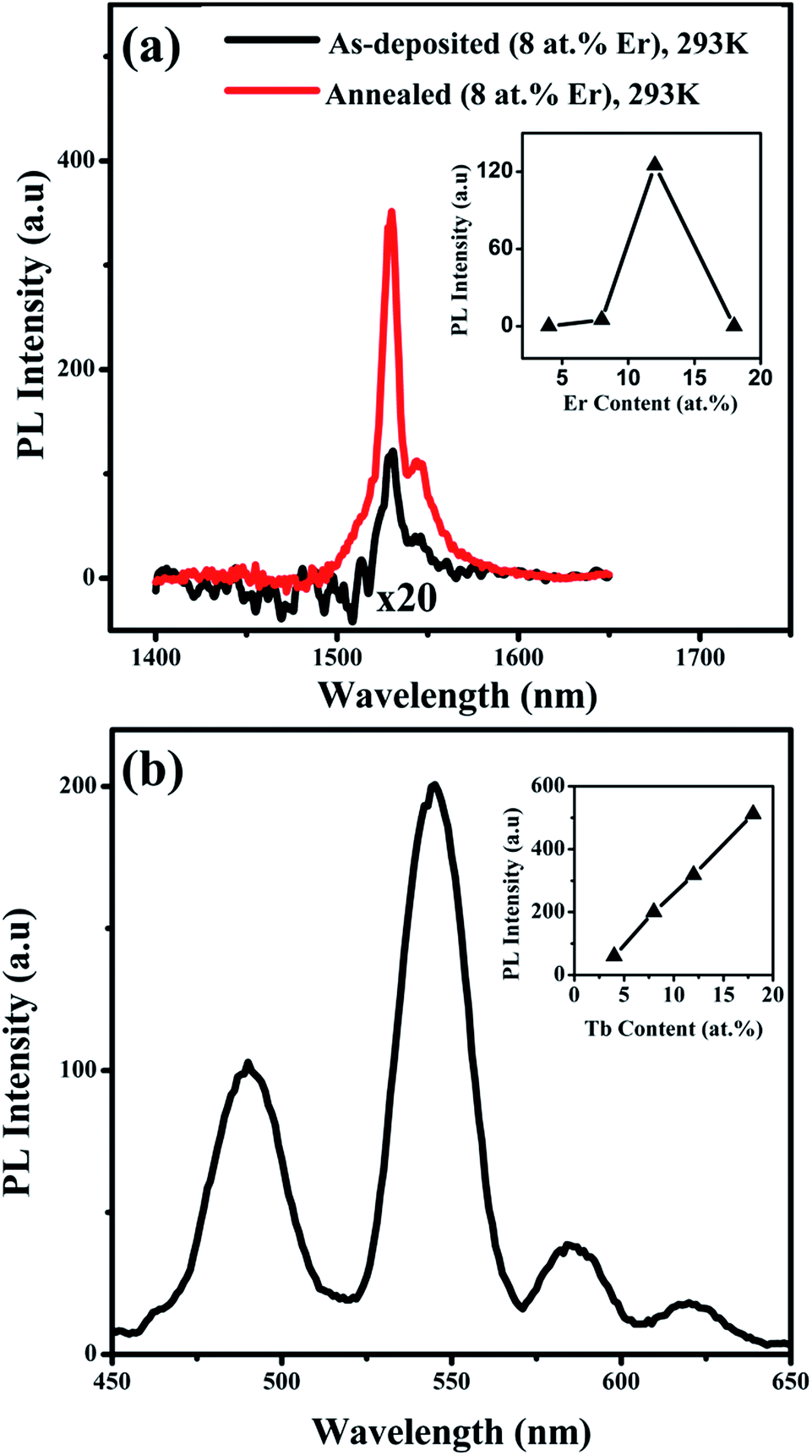 | ||
| Fig. 6 (a) PL emission spectrum obtained at RT from as-deposited Si/Er thin film (black) and PL emission spectrum at RT from annealed Si/Er thin film (red) using 325 nm laser source. The inset shows the variation of PL intensity at RT with the Er content in as-deposited Si/Er thin films. (b) The PL emission spectrum obtained at RT from the as-deposited (by applying −3 V vs. Pt) Si/Tb thin film. Inset shows the variation of PL intensity at RT with the Tb content in the deposits. | ||
The inset of Fig. 6a shows the variation of the PL intensity at RT against Er content in the as-deposited thin films. No PL emission was detected from thin film with less than 5 at% of Er and a very weak PL was obtained from the deposit containing 8 at% of Er. The maximum PL intensity was obtained from the thin film containing 12 at% of Er in the deposit. The higher Er3+ concentrations may lead to the formation of micro-clusters of erbium silicates such as Er2SiO5![[thin space (1/6-em)]](https://www.rsc.org/images/entities/char_2009.gif) 48,49 or Er2Si2O7,50,51 which are also luminescent in nature. However, it is observed that further increase in Er content than 12 at% results in the quenching of the PL emission. The Si/Er thin film containing 20 at% of Er did not give any detectable PL emission at RT. The higher concentration of Er in the thin film leads to the clustering of Er3+ ions which results in the concentration quenching of the luminescence due to the cross-relaxation processes.52,53 It is important to note here that the low temperature electrodeposition in RTILs leads to the incorporation of Er in amorphous Si (a-Si) and not in crystalline Si (c-Si) as in the case of most of the other growth techniques which could explain the observed intense emission signal. It is known that the a-Si offers better solubility for the Er3+ ions than the c-Si, and so a higher concentration of Er3+ can be achieved in a-Si compared to the c-Si.1,52,54 More importantly, it is reported that the a-Si clusters have a sensitizing effect on the Er3+ ions,55–57 which helps to improve the luminescence efficiency of Er3+ in Si. Therefore, the electrochemical co-deposition technique elaborated here is very important in this aspect as it gives the advantage of obtaining Er incorporated a-Si in a single step.
48,49 or Er2Si2O7,50,51 which are also luminescent in nature. However, it is observed that further increase in Er content than 12 at% results in the quenching of the PL emission. The Si/Er thin film containing 20 at% of Er did not give any detectable PL emission at RT. The higher concentration of Er in the thin film leads to the clustering of Er3+ ions which results in the concentration quenching of the luminescence due to the cross-relaxation processes.52,53 It is important to note here that the low temperature electrodeposition in RTILs leads to the incorporation of Er in amorphous Si (a-Si) and not in crystalline Si (c-Si) as in the case of most of the other growth techniques which could explain the observed intense emission signal. It is known that the a-Si offers better solubility for the Er3+ ions than the c-Si, and so a higher concentration of Er3+ can be achieved in a-Si compared to the c-Si.1,52,54 More importantly, it is reported that the a-Si clusters have a sensitizing effect on the Er3+ ions,55–57 which helps to improve the luminescence efficiency of Er3+ in Si. Therefore, the electrochemical co-deposition technique elaborated here is very important in this aspect as it gives the advantage of obtaining Er incorporated a-Si in a single step.
Contrary to the Si/Er thin film, no thermal annealing treatment is required for obtaining efficient PL from the Si/Tb thin films because of the inherent affinity of Tb towards the oxygen.41 The PL emission properties of the Si/Tb thin films were studied by excitation with 325 nm wavelength laser source. The PL spectrum obtained at RT from Si/Tb thin film deposited by applying −3 V (8 at% Tb) is shown in Fig. 6b. The spectrum shows emission bands in the visible wavelengths resulting from the radiative transitions between the intra 4f energy levels of the Tb3+ ions. In the spectra, four main PL bands can be identified where the most intense peak at 543 nm corresponds to the 5D4–7F5 transition. The other observed transitions are 5D4–7F6 (486 nm), 5D4–7F4 (583 nm), and 5D4–7F3 (620 nm). It is interesting to note here that no PL emission from the higher energy 5D3 is detected from the thin films, as the cross relaxation processes produces an increase in the population of 5D4 states at the expense of 5D3 state.58 The stark splitting in the PL bands is not clearly identifiable from the spectrum because of the setup spectral resolution as the wavelengths corresponding to each stark level are very close (541 and 545 nm) for the predominant PL band. The spectral shapes also depend on the local environment surrounding the Tb3+ ions, and such spectral shape is often observed in comparable materials.59,60
The inset of Fig. 6b compares the PL emission intensities at RT of Si/Tb thin films with different Tb concentrations in the deposit. It is clear that the PL intensity increases with the increase in Tb content in the deposits. As evident from the graph, the deposit containing the lowest Tb content (<5 at%) also shows a detectable PL emission. In contrast to the Si/Er thin films, Si/Tb thin film containing 15–20 at% of Tb shows the highest PL intensity. The oxides (Tb2O3 or Tb4O7) 61–63 of Tb formed at higher Tb3+ concentrations should have a significant contribution to the PL emission observed from the deposit. No concentration quenching effect is observed in the Si/Tb thin films till 20 at% of Tb content, which is the maximum RE content obtained by the current electrodeposition technique. The absence of concentration quenching phenomena in Si/Tb deposits could be due to the high penetration depth of Tb in Si64 and also to the high degree of oxidation of Tb in the deposit. It is reported that the presence of oxygen helps to reduce the segregation of RE in Si and makes the incorporation of it easier by forming RE–O complexes.65,66
4. Conclusions
In summary, a single step electrochemical method for the incorporation of RE ions (Er, Tb) in Si thin film using RTIL has been demonstrated for the first time. The electrodeposited Si/RE thin films are of good structural quality with uniform distribution of RE ions in the film. It is shown that the concentration of RE ions in the thin films can be easily tuned by adjusting the applied potential. Additionally, the electrodeposition of metallic Er and Tb from RTILs has been successfully demonstrated. The electrochemical co-deposition in RTIL results in the incorporation of RE ions directly in amorphous Si, the combination of which found to be efficient for optical applications. The PL measurements show strong luminescence emission at 1.53 μm from Si/Er thin films and in the visible wavelengths (450–650 nm) from Si/Tb thin films. The intense PL emissions at room temperature confirm the quality of the electrodeposited thin films for applications in opto-electronics. The method described provides a simple and low cost alternative for the RE incorporation in Si. The obtained results also prove the versatility of the RTILs as a solvent for electrodeposition of semiconductors and RE incorporated semiconducting materials.Conflicts of interest
There are no conflicts to declare.Acknowledgements
The authors would like to acknowledge Region Champagne-Ardenne, the DRRT Champagne-Ardenne and the European FEDER for the financial support through the Synapse project and their support of the Nano'mat platform.References
- A. J. Kenyon, Prog. Quantum Electron., 2002, 26, 225–284 CrossRef CAS.
- P. G. Kik and A. Polman, MRS Bull., 2013, 23, 48–54 CrossRef.
- A. Polman, J. Appl. Phys., 1997, 82, 1–39 CrossRef CAS.
- G. Chang-xin, Z. Wei-ping and S. Chao-shu, J. Lumin., 1981, 24, 297–300 CrossRef.
- J. D. B. Bradley and M. Pollnau, Laser Photonics Rev., 2011, 5, 368–403 CrossRef CAS.
- X. Huang, S. Han, W. Huang and X. Liu, Chem. Soc. Rev., 2013, 42, 173–201 RSC.
- J. De Wild, A. Meijerink, J. Rath, W. Van Sark and R. Schropp, Sol. Energy Mater. Sol. Cells, 2010, 94, 1919–1922 CrossRef CAS.
- M. E. Castagna, S. Coffa, M. Monaco, A. Muscara, L. Caristia, S. Lorenti and A. Messina, Mater. Sci. Eng., B, 2003, 105, 83–90 CrossRef.
- W. Gao, T.-k. Li, Y. Ono and S.-T. Hsu, J. Rare Earths, 2006, 24, 673–678 CrossRef.
- B. Zheng, J. Michel, F. Y. G. Ren, L. C. Kimerling, D. C. Jacobson and J. M. Poate, Appl. Phys. Lett., 1994, 64, 2842–2844 CrossRef CAS.
- F. Namavar, F. Lu, C. H. Perry, A. Cremins, N. M. Kalkhoran and R. A. Soref, J. Appl. Phys., 1995, 77, 4813–4815 CrossRef.
- S. Cueff, C. Labbé, J. Cardin, K. Hijazi, J.-L. Doualan, O. Jambois, B. Garrido and R. Rizk, Phys. Status Solidi C, 2011, 8, 1027–1032 CrossRef CAS.
- F. Gourbilleau, P. Choppinet, C. Dufour, M. Levalois, R. Madelon, C. Sada, G. Battaglin and R. Rizk, Phys. E, 2003, 16, 341–346 CrossRef CAS.
- F. Iacona, D. Pacifici, A. Irrera, M. Miritello, G. Franzò, F. Priolo, D. Sanfilippo, G. Di Stefano and P. G. Fallica, Appl. Phys. Lett., 2002, 81, 3242–3244 CrossRef CAS.
- A. Podhorodecki, J. Misiewicz, J. Wojcik, E. Irving and P. Mascher, J. Lumin., 2006, 121, 230–232 CrossRef CAS.
- J. E. Powell, Inorg. Chem., 1964, 3, 1070 CrossRef.
- S. Zein El Abedin, N. Borissenko and F. Endres, Electrochem. Commun., 2004, 6, 510–514 CrossRef CAS.
- R. Al-Salman, S. Z. El Abedin and F. Endres, Phys. Chem. Chem. Phys., 2008, 10, 4650–4657 RSC.
- N. Borisenko, S. Zein El Abedin and F. Endres, in Electrodeposition from Ionic Liquids, Wiley-VCH Verlag GmbH & Co. KGaA, 2008, pp. 147–165 Search PubMed.
- M. Bechelany, J. Elias, P. Brodard, J. Michler and L. Philippe, Thin Solid Films, 2012, 520, 1895–1901 CrossRef CAS.
- T. Munisamy and A. J. Bard, Electrochim. Acta, 2010, 55, 3797–3803 CrossRef CAS.
- Y. Nishimura and Y. Fukunaka, Electrochim. Acta, 2007, 53, 111–116 CrossRef CAS.
- A. L. Bieber, L. Massot, M. Gibilaro, L. Cassayre, P. Taxil and P. Chamelot, Electrochim. Acta, 2012, 62, 282–289 CrossRef CAS.
- S. K. Cho, F.-R. F. Fan and A. J. Bard, Angew. Chem., Int. Ed., 2012, 51, 12740–12744 CrossRef CAS PubMed.
- G. M. Haarberg, L. Famiyeh, A. M. Martinez and K. S. Osen, Electrochim. Acta, 2013, 100, 226–228 CrossRef CAS.
- H. Ohno, in Electrodeposition from Ionic Liquids, Wiley-VCH Verlag GmbH & Co. KGaA, 2008, pp. 47–82 Search PubMed.
- J. Mallet, F. Martineau, K. Namur and M. Molinari, Phys. Chem. Chem. Phys., 2013, 15, 16446–16449 RSC.
- J. Mallet, M. Molinari, F. Martineau, F. Delavoie, P. Fricoteaux and M. Troyon, Nano Lett., 2008, 8, 3468–3474 CrossRef CAS PubMed.
- F. Martineau, K. Namur, J. Mallet, F. Delavoie, F. Endres, M. Troyon and M. Molinari, IOP Conf. Ser.: Mater. Sci. Eng., 2009, 6, 012012 CrossRef.
- D. Kowalski, J. Mallet, S. Thomas, A. W. Nemaga, J. Michel, C. Guery, M. Molinari and M. Morcrette, J. Power Sources, 2017, 361, 243–248 CrossRef CAS.
- A. M. Elbasiony, M. Olschewski, E. Abedin, S. Zein and F. Endres, ChemElectroChem, 2015, 2, 1361–1365 CrossRef CAS.
- A. Lahiri, M. Olschewski, T. Carstens, E. Abedin, S. Zein and F. Endres, ChemElectroChem, 2015, 2, 571–577 CrossRef CAS.
- K. Binnemans, Chem. Rev., 2007, 107, 2592–2614 CrossRef CAS PubMed.
- L. J. Small, J. M. Sears, T. N. Lambert, T. J. Boyle and R. F. Hess, RSC Adv., 2016, 6, 89564–89571 RSC.
- L. J. Small, J. M. Sears, T. N. Lambert, T. J. Boyle and R. F. Hess, RSC Adv., 2016, 6, 89564–89571 RSC.
- T. Kimura, A. Yokoi, H. Horiguchi, R. Saito, T. Ikoma and A. Sato, Appl. Phys. Lett., 1994, 65, 983–985 CrossRef CAS.
- M. Gong, J. Shi, W. Wong, K. Shiu, W. Zheng and K. Cheah, Appl. Phys. A: Mater. Sci. Process., 1999, 68, 107–110 CrossRef CAS.
- G. Mula, T. Printemps, C. Licitra, E. Sogne, F. D'acapito, N. Gambacorti, N. Sestu, M. Saba, E. Pinna and D. Chiriu, Sci. Rep., 2017, 7, 5957 CrossRef PubMed.
- B. Gelloz, R. Mentek and N. Koshida, Phys. Status Solidi C, 2012, 9, 2318–2321 CrossRef CAS.
- N. K. Shah, R. K. Pati, A. Ray and I. Mukhopadhyay, Langmuir, 2017, 33, 1599–1604 CrossRef CAS PubMed.
- G. L. P. Berning, H. C. Swart and B. de Witt, Appl. Surf. Sci., 1993, 64, 1–7 CrossRef CAS.
- H. Isshiki, A. Polman and T. Kimura, J. Lumin., 2003, 102–103, 819–824 CrossRef CAS.
- S. Coffa, G. Franzò, F. Priolo, A. Polman and R. Serna, Phys. Rev. B: Condens. Matter Mater. Phys., 1994, 49, 16313–16320 CrossRef CAS.
- A. Polman, G. N. v. d. Hoven, J. S. Custer, J. H. Shin, R. Serna and P. F. A. Alkemade, J. Appl. Phys., 1995, 77, 1256–1262 CrossRef CAS.
- A. R. Zanatta and F. L. Freire, Phys. Rev. B: Condens. Matter Mater. Phys., 2000, 62, 2016–2020 CrossRef CAS.
- P. Favennec, H. l'Haridon, D. Moutonnet, M. Salvi and M. Gauneau, Jpn. J. Appl. Phys., Part 1, 1990, 29, L524 CrossRef CAS.
- J. Michel, J. Benton, R. Ferrante, D. Jacobson, D. Eaglesham, E. Fitzgerald, Y. H. Xie, J. M. Poate and L. Kimerling, J. Appl. Phys., 1991, 70, 2672–2678 CrossRef CAS.
- H. S. Kamineni, V. K. Kamineni, R. L. Moore, S. Gallis, A. C. Diebold, M. Huang and A. E. Kaloyeros, J. Appl. Phys., 2012, 111, 013104 CrossRef.
- J. Zheng, W. Ding, C. Xue, Y. Zuo, B. Cheng, J. Yu, Q. Wang, G. Wang and H. Guo, J. Lumin., 2010, 130, 411–414 CrossRef CAS.
- M. Miritello, P. Cardile, R. L. Savio and F. Priolo, Opt. Express, 2011, 19, 20761–20772 CrossRef CAS PubMed.
- M. Miritello, R. Lo Savio, F. Iacona, G. Franzò, A. Irrera, A. M. Piro, C. Bongiorno and F. Priolo, Adv. Mater., 2007, 19, 1582–1588 CrossRef CAS.
- D. J. Eaglesham, J. Michel, E. A. Fitzgerald, D. C. Jacobson, J. M. Poate, J. L. Benton, A. Polman, Y. H. Xie and L. C. Kimerling, Appl. Phys. Lett., 1991, 58, 2797–2799 CrossRef CAS.
- D. S. Lee, J. Heikenfeld, A. J. Steckl, U. Hommerich, J. T. Seo, A. Braud and J. Zavada, Appl. Phys. Lett., 2001, 79, 719–721 CrossRef CAS.
- T. Oestereich, C. Swiatkowski and I. Broser, Appl. Phys. Lett., 1990, 56, 446–447 CrossRef CAS.
- G. W. Adeola, H. Rinnert, P. Miska and M. Vergnat, J. Appl. Phys., 2007, 102, 053515 CrossRef.
- G. Franzò, S. Boninelli, D. Pacifici, F. Priolo, F. Iacona and C. Bongiorno, Appl. Phys. Lett., 2003, 82, 3871–3873 CrossRef.
- A. Meldrum, A. Hryciw, A. N. MacDonald, C. Blois, T. Clement, R. DeCorby, J. Wang and Q. Li, J. Lumin., 2006, 121, 199–203 CrossRef CAS.
- H. Amekura, A. Eckau, R. Carius and C. Buchal, J. Appl. Phys., 1998, 84, 3867–3871 CrossRef CAS.
- M. Klak, G. Zatryb, J. Wojcik, J. Misiewicz, P. Mascher and A. Podhorodecki, Thin Solid Films, 2016, 611, 62–67 CrossRef CAS.
- B. Kaleli, M. Kulakci and R. Turan, Opt. Mater., 2012, 34, 1935–1939 CrossRef CAS.
- L. Li, S. Wang, G. Mu, X. Yin and L. Yi, Sci. Rep., 2017, 7, 42479 CrossRef CAS PubMed.
- H. Choi, J. H. Kim, S.-s. Yi, B. K. Moon and J. H. Jeong, Journal of Alloys and compounds, 2006, 408, 816–819 CrossRef.
- S. V. Belaya, V. V. Bakovets, I. P. Asanov, I. V. Korolkov and V. S. Sulyaeva, Chem. Vap. Deposition, 2015, 21, 150–155 CrossRef CAS.
- D. E. Nazyrov, Semiconductors, 2006, 40, 630–631 CrossRef CAS.
- J. S. Custer, A. Polman and H. M. v. Pinxteren, J. Appl. Phys., 1994, 75, 2809–2817 CrossRef CAS.
- R. Serna, M. Lohmeier, P. M. Zagwijn, E. Vlieg and A. Polman, Appl. Phys. Lett., 1995, 66, 1385–1387 CrossRef CAS.
| This journal is © The Royal Society of Chemistry 2018 |