
Engineering two-dimensional layered nanomaterials for wearable biomedical sensors and power devices
Xianyi
Cao
 a,
Arnab
Halder
a,
Yingying
Tang
a,
Chengyi
Hou
*b,
Hongzhi
Wang
b,
Jens Øllgaard
Duus
a and
Qijin
Chi
*a
a,
Arnab
Halder
a,
Yingying
Tang
a,
Chengyi
Hou
*b,
Hongzhi
Wang
b,
Jens Øllgaard
Duus
a and
Qijin
Chi
*a
aDepartment of Chemistry, Technical University of Denmark, DK-2800 Kongens Lyngby, Denmark. E-mail: cq@kemi.dtu.dk; Fax: +45 45883136; Tel: +45 45252032
bState Key Laboratory for Modification of Chemical Fibers and Polymer Materials, College of Materials Science and Engineering, Donghua University, Shanghai 201620, P. R. China. E-mail: hcy@dhu.edu.cn
First published on 11th September 2018
Abstract
High-quality personalized medicine and health management have increasingly demanded wearable biomedical electronic devices (WBEDs) towards being more flexible and stretchable. This modern-life oriented trend has driven tremendous efforts from both academia and industrial enterprises devoted to research and development of new-generation WBEDs for improving the quality of home medicine. The development of such WBEDs crucially depends on design and assembly of new-types of materials. Thanks to superior physicochemical properties derived by their two-dimensional (2D) layered structural nature, 2D layered nanomaterials (2DLNs) hold notable advantages and are offering a promising material platform for energy, sensing, and wearable electronic applications. By using 2DLNs as versatile building modules, a number of technical breakthroughs have recently been achieved for manufacturing state-of-the-art 2DLNs-supported flexible/stretchable sensors and power devices, which could help WBEDs further achieve enhanced flexibility/stretchability and realize remarkable performance improvements. This review aims to offer timely and comprehensive evaluations of the current status, remaining challenges, and future perspectives of 2DLNs-supported wearable biomedical sensors and power devices, with the emphasis on the latest advancements and the significance of 2DLNs in device design and fabrication.
 Xianyi Cao | Xianyi Cao received his Bachelor's degree in Chemical Engineering and Technology from Harbin Institute of Technology, China. After receiving his Master degree in Food Chemistry in 2014 from Jilin University, China, he moved to the Department of Chemistry, Technical University of Denmark, where he is currently pursuing his PhD degree under the supervision of Profs. Qijin Chi and Jens Øllgaard Duus. His primary research interests are in design, synthesis and characterization of two-dimensional nanomaterials and their applications in flexible electronic devices for energy conversion and storage, chemosensors and biosensors. |
 Chengyi Hou | Chengyi Hou is currently an associate professor at Donghua University. He received his PhD degree in 2014, majored in materials science and engineering, from Donghua University, China. In 2014–2017, he was honored as a H. C. Ørsted-Marie Curie postdoc fellow with Prof. Qijin Chi working at Department of Chemistry, Technical University of Denmark, Denmark. He has engaged in the development of innovative methods and experimental approaches to address the key scientific and technical challenges related to scalable synthesis, processing and assembly of nanomaterial-based soft (bio)electronics. Dr Hou has explored the potential biomedical applications of several types of nanomaterials as electronic skin, micro-reactors, artificial muscle and three-dimensional biological scaffolds. |
 Qijin Chi | Qijin Chi received his PhD in analytical and physical chemistry from Changchun Institute of Applied Chemistry, Chinese Academy of Sciences. After his postdoc experiences as a DFG fellow in Germany and as a JSPS fellow in Japan, he joined DTU Chemistry, Technical University of Denmark (DTU), where he is currently an associate professor. Dr Chi is a member of several professional societies, notably as a member of the Danish Academy of Natural Sciences and a fellow of Royal Society of Chemistry (FRSC). His current research interests focus on design and chemical synthesis of nanostructured materials for their applications in electrochemistry, flexible and wearable chemical sensors and biosensors, electrocatalysis, and energy storage and conversion. |
1. Introduction
1.1. Wearable electronic devices for biomedical purposes
Wearable biomedical electronic devices (WBEDs) are a class of sensing devices that can be attached to human epidermal tissues and used to detect diverse signals (e.g., blood pressure, blood glucose, pulse rate, and motion) related to activities of the human body.1 If we take a broader perspective, then they could further include sensing devices that can monitor changes of surrounding indexes (e.g., air pollutants and pathogens) crucial to human health.2Fig. 1a shows typical health-related data that can be obtained from some representative WBEDs (Fig. 1b, left).3–8 These physiological and surrounding indexes can provide a wide range of clinical clues that are important for point-of-care (POC), disease prevention, early diagnosis, and rehabilitation therapy.1 With the rapid development of internet of medical things (IoMT) (Fig. 1c), WBEDs have shown great promise in reducing public healthcare costs and improving the quality of human life.9 The thriving market of WBEDs was estimated as $3.3 billion worldwide in 2015, and it is projected to reach $7.8 billion by 2020 with an average annual growth rate of 17.7%.10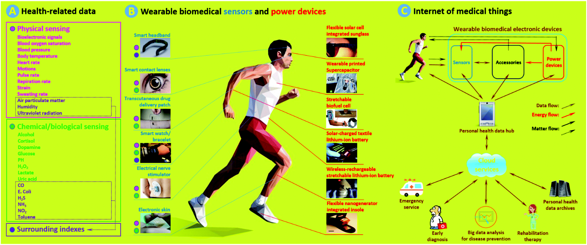 | ||
| Fig. 1 (a) Typical health-related data that can be obtained from WBEDs. (b) Representative wearable biomedical sensors (blue, left) and power devices (red, right). The coloured dots next to different sensors stand for probable sensing data types (pink: physical signal sensing, green: chemical/biological signal sensing, purple: surrounding index sensing) of corresponding sensors. (c) Schematic of a simple IoMT network. Matter flows with dotted-type dashes stand for: (1) some power devices such as biofuel cells and nanogenerators which need to acquire energy sources from a human body; (2) some accessories can execute simple medical procedures, such as transcutaneous drug delivery; (3) chemical/biological sensing require sampling from body fluid or exocrine secretion. Adapted from ref. 3–8 and 13–18 with permission. Copyright 2018, Nature Publishing Group. Copyright 2018, John Wiley & Sons. Copyright 2018, Royal Society of Chemistry. Copyright 2018, American Chemical Society. Copyright 2018, Elsevier. | ||
Considered from the angle of structural functionalities, WBEDs consist of two main functional units: sensors and power devices (Fig. 1c, upper right). Sensors are sensing components used for acquiring and recognizing various health-related physical and chemical/biological signals (Fig. 1b, left).3–8 Sensing performances are highly dependent on sensitive and specific recognition of sensors using intensity variation of monitored signals. Therefore, adopting functional materials with suitable physicochemical properties for fabricating sensors is an essential issue. In most instances, sensors are also integrated with some accessories, which are a series of auxiliary functional components capable of processing data and making specific responses, such as signal transducing/conditioning/indicating and actuated sampling/treating and data caching/communicating.11,12 Power devices (Fig. 1b, right) are responsible for providing required power to the whole WBEDs.13–18 Common power devices used in WBEDs include batteries, supercapacitors (SCs), and photovoltaics (PVs).19 Depending on specific working regions and power-supplying requirements, these power devices are suitably adopted and effectively integrated with sensors as well as other functional units. Recently, biofuel cells (BFCs) and nanogenerators (NGs) are also receiving increased attention since they are leading a new approach by which energy sources can be acquired from the human body itself.19,20
With regard to mainstream WBEDs currently dominating the global market, most of their sensors are still engineered and fabricated based on conventional printed circuit board (PCB) designs, which are mainly constituted by inorganic semiconductor (e.g., Si, Ge, GaAs) based electronic elements, printed metal (e.g., Cu, Al) wirings and resin-based materials.21 These components are generally quite rigid, making as-fabricated sensors lacking flexibility and stretchability. On the other hand, commonly employed power devices, such as Li-ion batteries (LIBs), are also rigid and planar. Their electrode active materials may detach from metal current collectors during repeated deformation, resulting in irreversible performance degradation.19 Due to this distinct structural mismatch between rigid/planar structural units and soft/curvilinear human body, WBEDs often fail to exhibit their optimal overall performances and provide sufficient comfortableness for users under potentially intense and frequent strain deformation.22 Thus, owing to urgent demands of next-generation WBEDs with better deformability and body compliance, worldwide academic and industrial circles are imminently eager to effectively integrate enhanced flexibility and stretchability into newly-developed wearable sensors and power devices. Specifically speaking, in addition to achieving those basic sensing/power-supplying performance indexes, sensors and power devices applied in next-generation WBEDs should also meet the following requirements: (1) they can function properly in a suitable elastic deformation range, and the broader the better; (2) even after several deformation processes, they can recover their mechanical and sensing/power-supplying performances without any obvious irreversible degradation.23
Aiming to address these, there are generally three main engineering strategies. First, adopting cutting-edge micro- and nanomanufacturing technologies to process conventional PCB materials in unconventional ways could provide some alternative solutions. This is based on the fact that with decreasing material thickness, material bending stiffness also will decrease. Therefore, compared with corresponding bulk rigid materials, micro- and nanostructures could be more flexible.24 A previous study has shown that the flexural rigidity of Si nanomembranes with 2 nm thickness can be theoretically 15 orders of magnitude smaller than those of Si wafers with 200 μm thickness.25 Unfortunately, most materials used in sensors and power devices of conventional WBEDs cannot achieve stretchability by this way. Integration of newly-emerging organic transistors and base materials, as well as some bio-inspired stretchable substrates, could help ameliorate this problem to some extent.26–28 Second, inspired by diverse natural structures and phenomena, many fascinating structural designs have been utilized to endow some components of WBEDs (especially power devices) with greatly enhanced stretchability and deformability, such as buckling design, serpentine design, origami design, and textile design.19 However, these designs are non-intrinsic, which means they cannot change flexibility and stretchability of every single structural unit. When adopting these designs, how to realize effective structural integration of different functional units without affecting sensing performances and user comfortableness is also worthy of consideration. Third, developing new classes of intrinsically flexible/stretchable materials and realizing their effective replacement for rigid materials used in sensors and power devices of conventional WBEDs have received much attention. Diverse one-dimensional (1D) nanomaterials as well as three-dimensional (3D) nanomaterials/nanostructures have been employed for constructing functional units of several novel prototypes of WBEDs.19,29–34 Many of them have achieved quite noticeable improvements on overall device performances and offer potential promise to further technological upgrades. However, these studies remain in infant stages of development and still have some intrinsic drawbacks related to materials and processing technologies.
Although all of above strategies are quite useful for the development of WBEDs with better deformability and body compliance, intrinsic material flexibility/stretchability is still a predominant property since it determines the theoretical upper limit of specific component performances. Thus, both user groups and business circles are urgently expecting a new technological revolution that can bring intrinsic performance breakthroughs in the area of WBEDs, and such revolution could most likely be invoked by designing and developing new classes of materials with desirable structural and functional properties. To this end, tremendous efforts are demanded from physicists, chemists, and material scientists, in addition to researchers working in the areas of biomedical science and engineering.
1.2. Why use two-dimensional layered nanomaterials
As mentioned above, a critical step in developing high-performance WBEDs is to explore advanced functional nanomaterials used for constructing different functional units of WBEDs. As a novel family of nanomaterials, two-dimensional (2D) layered nanomaterials (2DLNs) are becoming a major focus of this stage from both fundamental and application points of view. Since Novoselov, Geim and coworkers presented their Nobel Prize awarded (Physics, 2010) groundbreaking research on isolating graphene (the first 2DLN) monolayers from graphite bulk crystals,35 intense research endeavors have been paid worldwide to comprehend the intrinsic characteristics of 2DLNs and explore their cutting-edge applications in micro- and nanoelectronics, catalysis, and bioengineering as well as energy storage and conversion.36Defined by their structural features, 2DLNs are a class of nanomaterials with a well-ordered 2D planar structure (lateral size >100 nm) but only one- or few-atom-layer thick (typical thickness <5 nm).37 Represented by graphene, 2DLNs are derived from a series of layer-structured compounds.38 These layer-structured compounds can be structurally regarded as orderly stacking of corresponding 2DLNs in the direction perpendicular to 2D planes, and with strong intraplane chemical bonding but weak interplane van der Waals (vdW) interactions. 2DLNs have many extraordinary physicochemical properties that are far different from those of their corresponding bulk materials and which are attributed to their unique structural characteristics.39 For example, monolayer graphene possesses an ultrathin and planar nanostructure comprised of sp2-bonded carbon atoms arranged in a honeycomb lattice.40 Owing to this unique structure, it can exhibit many fascinating properties such as high theoretical specific surface area (2630 m2 g−1), superior carrier mobility (∼200![[thin space (1/6-em)]](https://www.rsc.org/images/entities/char_2009.gif) 000 cm2 V−1 s−1), magnificent optical transmittance (∼97.7%), ultrahigh intraplane mechanical strength (∼1.0 TPa, Young's modulus), high thermal conductivity (3080–5150 W m−1 K−1), and room-temperature quantum hall effect,41 which make graphene highly attractive in developing advanced energy, electronic, and biomedical applications. In spite of its superior properties, graphene has also shown some disadvantages. For instance, lack of an intrinsic band gap is a vital drawback of graphene, which restricts its extensive application in semiconductor electronic/optoelectronic areas.41 Fortunately, this drawback not only has motivated the research on graphene-based nanocomposites42 and heteronanostructures43 as well as interface functionalization and band gap engineering, but also triggered enormous efforts towards the design, synthesis, and applications of other 2DLNs.44 These ‘beyond graphene’ 2DLNs (Fig. 2) span from hexagonal boron nitride (h-BN), transition metal oxides (TMOs: ZnO, WO3, MnO2, TiO2, Co3O4, etc.), transition metal carbides (MXenes: Ti3C2Tx (T: surface functional groups), Ti2CTx, etc.), layered metal hydroxides (LMHs: Ni-LMH, NiFe-LMH, MgFe-LMH, etc.), transition metal chalcogenides (TMCs: MoS2, ReS2, WSe2, MoTe2, etc.), perovskites (BaTiO3, CH3NH3PbI3, etc.), graphitic carbon nitride (GCN), elemental graphene analogues (silylene, germanene, phosphorene, antimonene, etc.), to bio-inspired carbons.45–53
000 cm2 V−1 s−1), magnificent optical transmittance (∼97.7%), ultrahigh intraplane mechanical strength (∼1.0 TPa, Young's modulus), high thermal conductivity (3080–5150 W m−1 K−1), and room-temperature quantum hall effect,41 which make graphene highly attractive in developing advanced energy, electronic, and biomedical applications. In spite of its superior properties, graphene has also shown some disadvantages. For instance, lack of an intrinsic band gap is a vital drawback of graphene, which restricts its extensive application in semiconductor electronic/optoelectronic areas.41 Fortunately, this drawback not only has motivated the research on graphene-based nanocomposites42 and heteronanostructures43 as well as interface functionalization and band gap engineering, but also triggered enormous efforts towards the design, synthesis, and applications of other 2DLNs.44 These ‘beyond graphene’ 2DLNs (Fig. 2) span from hexagonal boron nitride (h-BN), transition metal oxides (TMOs: ZnO, WO3, MnO2, TiO2, Co3O4, etc.), transition metal carbides (MXenes: Ti3C2Tx (T: surface functional groups), Ti2CTx, etc.), layered metal hydroxides (LMHs: Ni-LMH, NiFe-LMH, MgFe-LMH, etc.), transition metal chalcogenides (TMCs: MoS2, ReS2, WSe2, MoTe2, etc.), perovskites (BaTiO3, CH3NH3PbI3, etc.), graphitic carbon nitride (GCN), elemental graphene analogues (silylene, germanene, phosphorene, antimonene, etc.), to bio-inspired carbons.45–53
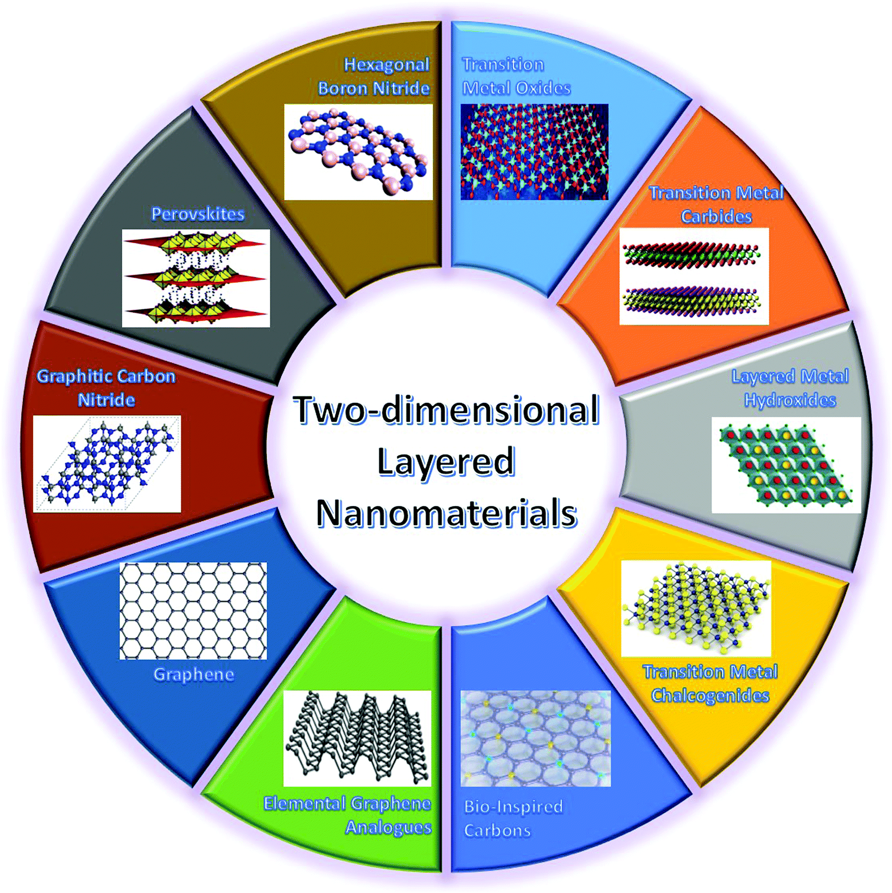 | ||
| Fig. 2 Highlights of major types of 2DLNs with their representative crystal structures illustrated. Adapted from ref. 45–53 with permission. Copyright 2018, Nature Publishing Group. Copyright 2018, American Chemical Society. Copyright 2018, Royal Society of Chemistry. | ||
The 2DLN portfolio can be enriched further since many elemental and compound nanomaterials with a 2D layered structure are not covered yet. This continually expanded material library can further cover a wide range of beneficial physicochemical properties, which could boost diverse state-of-the-art applications, especially WBEDs, achieving better comprehensive performances.54 A typical example is the obstacle of lacking band gap in graphene has been successfully overcome by other 2DLNs with their band gap range sufficiently covered from 0 to more than 5 eV (Fig. 3), which is of great significance to the design of diversified high-performance semiconductor components for sensor applications.55 Moreover, ultrahigh specific surface area and abundant redox active sites as well as possibilities of further structural regulation of some 2DLNs have endowed them with great potential as advanced electrode active materials of batteries, SCs, and BFCs.19,56,57 Besides, engineering advanced 2DLN based composites by hybridizing 2DLNs with other functional materials could effectively surmount the deficiencies of individual constituents, optimize their structures and properties, and even generate novel functionalities that the individual constituents do not possess.42,58,59
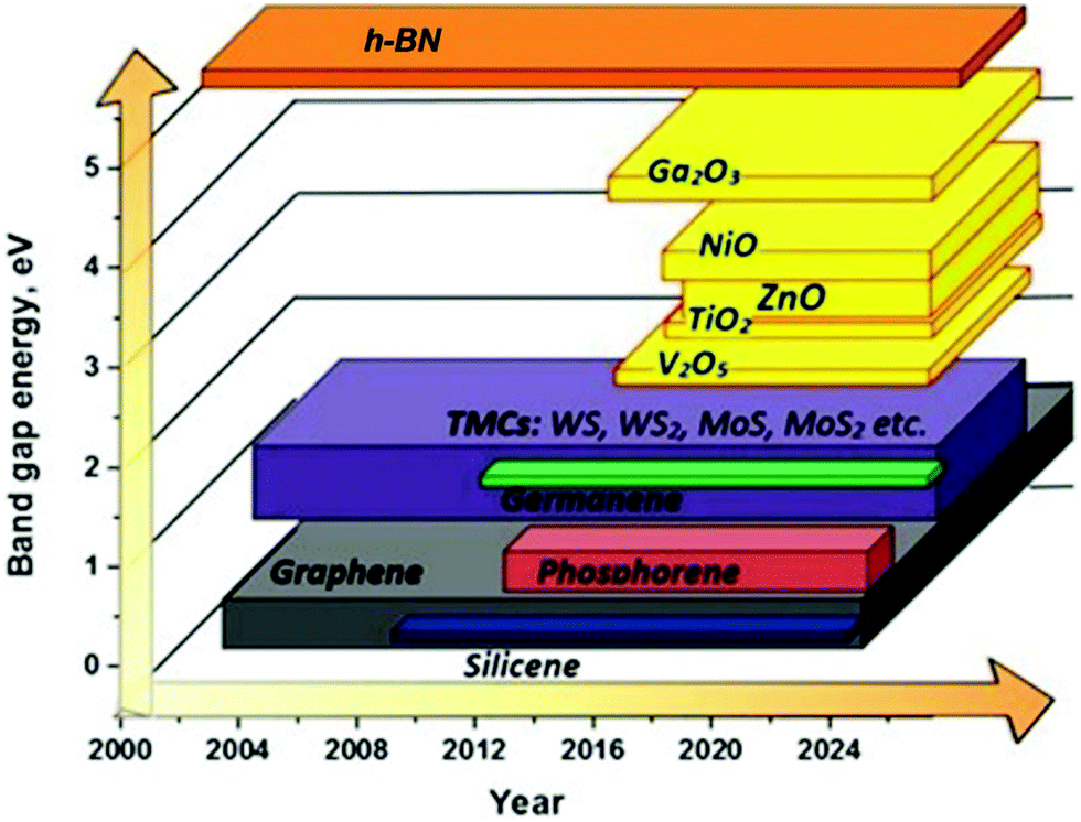 | ||
| Fig. 3 Illustration of the family evolution of 2DLNs showing the representative band gap values of various 2DLNs on the vertical axis plotted against time on the horizontal axis. Reproduced from ref. 55 with permission. Copyright 2018, MDPI. | ||
From the perspective of WBED development, compared with their counterparts in other dimensionalities, the 2DLN family possesses many unique and highly-targeted superiorities. First, the atomic thickness and large lateral size of 2DLNs endow them with ultrahigh theoretical specific surface areas, which attracts a lot of attention when developing high-performance flexible electrodes for energy conversion and storage, as well as other interface-active applications.23,36,42,60 Second, high exposure of 2DLN atoms provides more possibilities for surface modification/functionalization and elemental doping, which can help realize flexible regulation on material properties such as band gap.44,61 Third, combining thin-film-like macroscopic properties with quantum confinement microscopic features, 2DLNs possess both high compatibility with conventional semiconductor processing technologies and novel electronic/optoelectronic characteristics stemming from quantum effects.62 Fourth, by filtration, spin-coating, spray-coating or inkjet-printing, many solution-processed 2DLNs can be facilely fabricated into free-standing continuous homogenous films, which is of great significance to cost-efficient industrial manufacturing of electronic/optoelectronic components.12 Last, their strong intraplane chemical bonding and ultrathin thickness offer them terrific mechanical strength, flexibility, and optical transparency, all of which are quite favorable properties in developing flexible and transparent electronics for wearable applications.62
It should be noted that inspired by 2DLNs, 2D non-layered nanomaterial (2DNLN) research is also becoming a very hot area recently.37,63 The principal difference of 2DNLNs with 2DLNs is that 2DNLNs (e.g., metals, some TMOs, TMDs, and perovskites with special crystalline phases) form strong chemical bonding in three dimensions, reflecting the non-layered nature of their macroscopic bulk phase. Although 2DNLNs may bring up some new functionalities and advantageous properties, they still have some unshakable superiorities. On one hand, compared with 2DNLNs, it is still much easier to synthesize them with well-controlled thickness and surface state owing to their basic structural features, which will benefit precise tuning of electronic/optoelectronic properties.37,44 On the other hand, current synthetic strategies of 2DNLNs are widely based on template synthesis or substrate-supported growth. Realizing high-quality template removal and product transfer remains a critical challenge.37,63 On the contrary, facile, efficient and low-cost solution processability of 2DLNs make them more favorable for scalable production.44 All of the above have provided sufficient prerequisites for the bright prospect of developing high-performance 2DLNs-supported WBEDs.
In the following discussion, we will first briefly describe common synthetic methods for preparing the aforementioned 2DLNs. Then, we will give an overview of a series of prototypes/products of 2DLNs-supported new-fashioned wearable biomedical sensors (as well as sensor accessories), power devices, and typical integrated systems composed of both of them. At the end, we also provide some personal viewpoints on current challenges and possible countermeasures and give an outlook for this promising field.
2. Syntheses of two-dimensional layered nanomaterials
Various preparation techniques, including mechanical exfoliation (ME),35 liquid exfoliation (LE),64 chemical vapor deposition (CVD),65 physical vapor deposition (PVD),66 electrochemical deposition (ECD),67 wet chemical synthesis (WCS),68 reagent-free electrophoretic synthesis,69 and unzipping of 1D nanomaterials,70 have been developed for the fabrication of 2DLNs (Fig. 4). From the perspective of methodology, these methods can be largely classified into three categories, i.e., ‘top-down’, ‘bottom-up’ and other approaches.69,71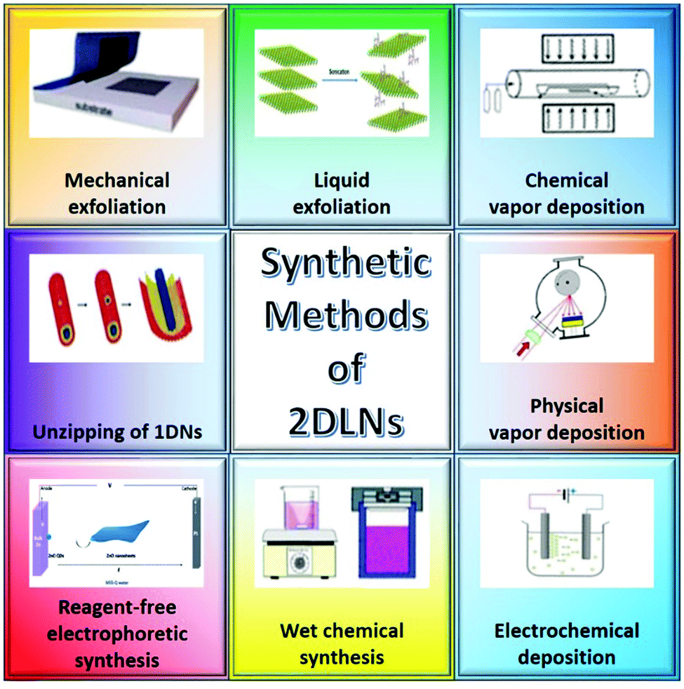 | ||
| Fig. 4 Schematic of various synthetic methods of 2DLNs. Adapted from ref. 69 and 71 with permission. Copyright 2018, American Chemical Society. Copyright 2018, Royal Society of Chemistry. | ||
2.1. ‘Top-down’ approach
The ‘top-down’ approach relies on the exfoliation of layered bulk crystals into single- or few-layer nanosheets, in which various driving forces are used to break vdW interaction between stacked layers.ME was first applied to peel off highly oriented pyrolytic graphite repeatedly with scotch tape to separate monolayer graphene.35 Since then, this method has evolved as a typical top-down strategy for obtaining atomically thin 2DLN sheets from layered bulk materials, such as MoS2,72 WSe2,73 and h-BN.74 This method is relatively fast, convenient and economical, and the as-prepared 2DLNs can exhibit large lateral size, excellent crystallinity, and few defects, thus making them very suitable for investigation of their intrinsic properties and prototype validation of devices.72 However, mass production and high yield cannot be achieved by this method, which is its main limitation. Thus, the use of this method is restricted to laboratory-scale studies.
LE is a reliably alternative method, which can significantly promote ‘top-down’ synthesis to a large scale.64 In this method, synthesized samples or commercial chemicals are sonicated in an appropriate solvent for a period to exfoliate the bulk materials into mono- or few-layer nanosheets. This method was first used for the synthesis of graphene oxide (GO) from pre-oxidized graphite.75 After that, some organic solvent, surfactant, or polymer assisted LE methods were developed to prepare diverse 2DLNs, such as graphene,76 GCN,77 TMCs,78 TMOs,79 and h-BN.80 By choosing appropriate intercalators, exfoliation efficiency during sonication could be greatly improved by weakening the vdW interactions between atomic layers, and meanwhile desired functionalization to the 2DLNs could also be achieved.81 However, these methods, in general, suffer from poor controllability of layer numbers and low yields of monolayer nanosheets.82 Li+ intercalation was employed for liquid exfoliating TMCs, which has been validated to be very efficient for synthesizing monolayer nanosheets with high yields.83 An electrochemical Li+ intercalation method was proposed to accurately regulate the intercalation process, by which high-quality TMCs and h-BN monolayer products were obtained on a large scale.83 A tetrabutylammonium hydroxide-assisted intercalation method was also reported to exfoliate layered perovskite-type niobate.84 It should be noted that all above-mentioned LE methods could potentially cause a high density of surface defects and stubborn impurities, and pose technical difficulties to separate co-existing monolayer and multilayer nanosheets.37
2.2. ‘Bottom-up’ approach
The bottom-up approach can realize the gradual growth of 2DLNs directly in solution (i.e., WCS) or on suitable substrates/templates/interfaces by vapor deposition (i.e., CVD/PVD), or electrochemical deposition (i.e., ECD).Among ‘bottom-up’ strategy-based synthetic methods, CVD and PVD are two representative techniques widely used in the semiconductor industry for fabricating various solid thin films.85 By utilizing CVD or PVD, high-quality 2DLNs with large lateral size, few surface defects, and tunable layer numbers can be deposited onto different substrates, which can be further used for large-scale fabrication of various electronic devices.86 In a typical CVD process for 2DLN synthesis, gaseous precursors react with each other or decompose in a CVD reaction chamber, depositing 2DLNs on desired surfaces. High-quality MoS2 nanosheets were successfully synthesized on insulating SiO2 substrates by a two-step approach.65 A Mo thin layer was first pre-deposited on the substrate, followed by introducing sulfur vapor into a tube furnace to react with the Mo layer. Monolayer h-BN was also successfully synthesized on Ni(111) by CVD through the thermal decomposition of B-trichloroborazine.87
Unlike CVD, a PVD-based method for 2DLN synthesis employs simpler physical processes (e.g., laser ablation, electron bombardment, electric arc, electrical resistance heating, glow discharge plasma sputtering) to vaporize surface molecules of a bulk material target, followed by depositing 2DLN on suitable surfaces. Pulsed laser deposition (PLD) is a representative PVD method, by which laser pulses are used to strike and ablate the bulk material target.66 This method has been used for preparing 2D MoS2,66 GaSe,88 and phosphorene.89 During the process, several experimental parameters, such as laser spot size, laser intensity, substrate temperature, incident angle, and ablation time, are crucial for determining quality of the 2DLNs films. A filtered cathodic vacuum arc can be employed to deposit amorphous carbon thin films on catalytic Ni films grown on SiO2–Si substrates.90 After a post-annealing process in vacuum, the obtained carbon thin films are converted into large-area few-layer graphene. In general, both CVD and PVD are suitable for large-scale device fabrication. However, it should be noted that both of them require quite high equipment and consumables costs.37
In contrast, ECD offers a feasible and low-cost technique for preparation of 2DLNs. By varying applied potential, current, and time, the thickness of 2DLN films can be effectively tuned. Some TMCs and TMOs, such as MoSe291 and NiCo2O4,92 have been successfully synthesized by this method. In most cases, however, it is challenging to obtain mono- or few-layer 2DLN-based thin films by this method, plus nanosheet quality and integral film uniformity needs to be improved.92
WCS is another one of the most traditional and simplest methods to prepare materials from liquid phase, by which a variety of 2DLNs have been synthesized under mild conditions simply and cost-effectively.37 Hydro-/solvothermal synthesis, an inspiration originated from geology, is an evolved WCS route in which liquid phase crystallization occurs under relatively high temperature and pressure. In laboratory research, a typical hydro-/solvothermal synthetic process is generally conducted in an autoclave, which is a hermetically sealed vessel made of chemically inert materials that can resist high temperature and pressure for a prolonged period of time (several hours to days). The most significant advantage of hydro-/solvothermal synthesis over other WCS methods is that various 2DLNs can be prepared with high purity, better dispersity, and optimized crystalline microstructures. Many crystalline phases difficult to create under ambient conditions can be easily prepared using this technique. Combined with its facile solution processability, this technique has great potential for large-scale production. This high-yield and low-cost approach has evolved into an extensively used synthetic technique by which diverse 2DLNs with high crystallinity have been synthesized, such as TMCs,68 TMOs,55 and LMHs.93 However, it is noticed that even employing a quite effective hydro-/solvothermal process, products containing a high proportion of monolayer sheets are still rare. In addition, surfactants are often needed to achieve a nanoscale control of product morphology.68
2.3. Other approaches
In addition to the above-mentioned preparation techniques, some other synthesized methods cannot be simply classified into ‘top-down’ or ‘bottom-up’ approaches. Very recently, Hou and co-workers developed an ultra-green reagent-free electrophoretic method for cost-effective and rapid preparation of 2D few-atom-thick TMO nanosheets that can be further transformed into nanofilms.69,94 The method combines top-down building block synthesis and bottom-up electrophoretic assembly in aqueous solutions under ambient conditions using only bulk metal and water as starting materials without involving any additional reagents. By this method, several kinds of 2D TMO (including ZnO and Fe2O3) nanosheets can be synthesized simply and rapidly. These 2D few-atom-thick TMO nanosheets exhibit freestanding and flexible features, with plenty of exposed polar facets and large ratios of lateral size to thickness (>10000). Unzipping of 1D nanomaterials (1DNs) is another newly emerging distinct method for 2DLN preparation. Not belonging to either ‘top-down’ or ‘bottom-up’ approaches, this method seems more relevant to be described as a sort of spatial structure adjustment. By this method, graphene nanoribbons were prepared for the first time from multi-walled carbon nanotubes (CNTs).70 Recently, this method was also adopted for synthesizing h-BN95 and WS296 nanosheets.
2.4. A comparison of main synthetic approaches
Although 2DLNs can be synthesized via different approaches, for the synthesis of a specific 2DLN, the structure, quality, and properties of its final product are highly dependent on the adopted method. On the other hand, considering both basic properties of as-synthesized 2DLNs and the perspective of their industrialized applications, different synthetic methods also have their own strengths and weaknesses. For instance, the mainstream synthetic routes of graphene include ME, CVD, and oxidation–exfoliation–reduction. ME is capable of producing high-quality graphene with micrometer-scale lateral size and few defects, whose structures, constituents, and properties are relatively closer to those of perfect graphene, thereby very suitable for fundamental research.72 However, as we have summarized, extremely low yields and poor size controllability make ME virtually impossible for mass production. The quality of CVD-synthesized graphene can be on a par with that of ME-prepared graphene.37 Besides, CVD can even produce graphene with centimeter-scale lateral size and offer better thickness tunability.37 Furthermore, CVD processability endows graphene with sufficient potential to be integrated into current mature semiconductor technologies.85 Nevertheless, high production cost and deficient process technologies are still two major barriers for CVD-synthesized graphene.37 Compared with ME that directly obtains graphene from graphite, oxidation–exfoliation–reduction employs an indirect route.97 First, graphite is oxidized into graphite oxide in liquid phase. Then, graphite oxide is liquid-exfoliated into GO. After that, by thermal, chemical, or electrochemical reduction, GO is finally reduced to the final product, the so-called reduced GO (rGO). Although rGO obtained from oxidation–exfoliation–reduction is deemed as a member of the graphene family, it has unneglectable differences with graphene produced from ME or CVD.97 Due to increased defect concentration and the unavoidable residual of oxygen-containing functional groups, rGO largely deviates from the perfect graphene structure. The mechanical and electronic properties of rGO are thereby significantly inferior to those of graphene produced from ME or CVD.97,98 However, oxidation–exfoliation–reduction is a highly scalable method for graphene production with high yields and adequate processing convenience, which can lower production cost and realize kilogram-scale production.98,99 This is significant for exploring advanced energy storage applications that could make use of graphene on a relatively large scale. Besides, abundant oxygen-containing functional groups of GO provide a greater probability of engineering diverse graphene-based 2D nanocomposites.42One cannot expect there is such a 2DLN whose properties can perfectly fulfill various demands in different application areas. For all above-mentioned synthetic methods, some drawbacks also exist for each of them. The above discussion aims to remind researchers/engineers when adopting a 2DLN for a specific application purpose, all three key aspects including material properties, device requirements, and production scalability/costs should be soundly considered before making a final choice. A comprehensive comparison of various primary synthetic methods for 2DLNs is summarized in Table 1. But, there are still some novel and distinct synthetic methods of 2DLNs, which are not included there. Although some high-quality 2DLNs have been produced by these methods, they either fail to achieve high yields for large-scale applications, or require quite high raw material and equipment costs, thereby requiring further improvements. Moreover, CVD, WCS, and thermal annealing are three frequently used techniques for synthesizing various advanced 2DLN based composites, whose optimized structures, enhanced performances, and newly-emerging functionalities could help 2DLNs further enlarge their application scopes and improve their application potentials. More detailed introductions related to syntheses of 2DLNs and their composites can be found in several previous reviews.86,105
| Synthetic method | Brief description | Advantage | Disadvantage | 2DLN |
|---|---|---|---|---|
| a For LE by direct sonication. b For LE with an oxidation–reduction intercalation pretreating process. c For hydrothermal/solvothermal syntheses. d For unzipping 1DNs by direct oxidation under high temperature. e For unzipping 1DNs by intercalation–exfoliation strategy. | ||||
| Mechanical exfoliation | Use adhesive Scotch tapes to cleave layered bulk crystals and leave mono- or few-layer 2DLNs on a substrate | High quality | Labor intensive | Graphene35 |
| Few structural defects | Time-consuming | MoS2, WSe272 | ||
| Relatively large lateral size | Extremely low yield | WSe2, TaS2, TaSe273 | ||
| Low cost | Non-massive production | h-BN74 | ||
| Glue residual | ||||
| Liquid exfoliation | Exfoliate layered bulk crystals by direct sonication in solvents or in presence of surfactants or polymers, or adopt an intercalation pretreating process before sonication | Solution processability | Relatively small lateral size | GO75 |
| Massive production | Weak controllability of layer numbera | Graphene76 | ||
| Low cost | Low yield of mono- or few-layera | GCN77 | ||
| Simplicity | Surfactants required frequentlya | MoS2, WS2, NbSe2, h-BN78 | ||
| High yield of mono- or few-layer 2DLNsb | Some structural defectsb | MoO379 | ||
| h-BN80 | ||||
| NbSe2, h-BN83 | ||||
| Chemical vapor deposition | One or more precursors decompose and/or react under vapor state, depositing 2DLNs on exposed substrate surfaces | High quality | High temperature | MoS265 |
| Very large lateral size | High vacuum | h-BN87 | ||
| Few structural defects | High cost | Graphene100 | ||
| Massive production | Time-consuming | |||
| Excellent controllability of layer number | Complicity | |||
| Physical vapor deposition | Employ physical processes to vaporize surface layer molecules of a bulk material target, followed by depositing 2DLNs on exposed substrate surfaces | High quality | High vacuum | MoS266 |
| Large lateral size | High cost | GaSe88 | ||
| Few structural defects | Complicity | Phosphorene89 | ||
| Massive production | ||||
| Fast processing | ||||
| Electrochemical deposition | Use electrochemical reactions to propel the redox of precursors and deposit 2DLNs on electrode surface | Solution processability | Low quality | MoSe291 |
| Massive production | Weak controllability of layer number | NiCo2O492 | ||
| Low cost | Hardly obtain mono- or few-layer 2DLNs | Ti3C2101 | ||
| Simplicity | Many structural defects | |||
| Wet chemical synthesis | Direct synthesize 2DLNs in liquid phase | Solution processability | Surfactants required frequently | Bio-inspired 2D carbon53 |
| Massive production | Some structural defects | MoS268 | ||
| Low cost | Relatively high temperature and pressurec | MnO2102 | ||
| Simplicity | Ni-LMH103 | |||
| CsPbBr3104 | ||||
| Reagent-free electrophoretic synthesis | Combine the anodic oxidation with electric-field-induced assembly upon electrolysis of water | Solution processability | Some structural defects | ZnO69 |
| No chemicals | Fe2O394 | |||
| Low cost | ||||
| Simplicity | ||||
| Unzipping of 1DNs | Unzip 1DNs into 2DLNs by direct oxidation under high temperature or intercalation–exfoliation strategy | Simplicity | Some structural defects | h-BN95 |
| Massive production | Low yieldd | WS296 | ||
| Solution processabilitye | High temperatured | |||
| Weak controllability of layer numberd | ||||
| Small lateral size especially in widthe | ||||
In addition, current industrial-grade techniques still suffer from intractable dust and liquid waste as well as other potential environmental pollution risks. With on-going technology upgrading, we expect that revolutionary preparation techniques will be brought forward to produce environmentally-friendly diverse 2DLN products with excellent functional properties, large scale, and low cost. These advanced production techniques will undoubtedly help lay a solid foundation for developing future cutting-edge applications represented by 2DLNs-supported WBEDs.
3. Two-dimensional layered nanomaterials supported wearable sensors for biomedical applications
As previously discussed, sensing objects of WBEDs can be largely classified into two signal types: i.e., physical sensing and chemical/biological sensing. Physical sensing aims to detect variations of physical (e.g., mechanical, thermal, optical, electrical) signals around target organs or areas. For example, it can be directly used for monitoring body motion,106,107 body temperature and heart rate,108 as well as ultraviolet (UV) emission109 and humidity110 around a human body. Chemical/biological sensing is generally based on molecular recognition behaviors induced by chemical, electrochemical and biological reactions. It can be applied for probing signals of various chemical/biological molecules (e.g., glucose, H2O2, lactate) in body fluids, exocrine secretions, and surroundings.108,111 Besides, there are still many accessories that function with sensors synergistically for improving sensing performances or performing specific tasks. For example, in most cases, sensors need to be integrated with transducing systems (e.g., field-effect transistors (FETs)), which can transform or modulate as-collected original signals into more easy-to-read forms.55 By integrating a series of physical and biological sensors with thermoresponsive microneedles, well-controllable thermally-actuated transcutaneous drug delivery can also be achieved by monitoring-therapy all-in-one devices for coping with diabetes.5 In this chapter, we focus on several recent advances achieved by 2DLNs-supported wearable sensors for both physical and chemical/biological sensing, as well as introduce some 2DLNs-supported accessories including transducers, amplifiers, memristors, signal indicators, actuators, and conductive substrates.3.1. Two-dimensional layered nanomaterials supported wearable biomedical sensors for physical signal sensing
Some physical signals, such as body temperature, pulse rate, respiration rate and blood pressure, can well reflect basic running conditions of a human body. Monitoring these physical signals is thus of vital importance for health administration and disease prevention.108 In this section, wearable sensors for monitoring diverse physical signals are reviewed. Distinguished by specific signal types, their working mechanisms and corresponding functions of adopted 2DLN constituents are emphatically introduced respectively.2DLNs with excellent thermosensitivity or thermoconductivity are being widely explored for their potential applications in advanced personal thermal monitoring and management.113–116 Hereinto, graphene-family materials supported temperature sensors have received most attention based upon their significant capacitance/resistivity changes under temperature variations.108 Besides, superior thermoconductivity and physicochemical stability of graphene-family materials could help achieve better sensitivity and anti-interference performance. Sadasivuni and coworkers reported a flexible, partially transparent and efficient temperature sensor based on a composite film consisting of rGO and a naturally abundant, environment-friendly and biocompatible polymer, cellulose.117 rGO nanosheets were first synthesized by partial reduction of GO through low-temperature annealing. Then, a rGO–cellulose composite solution was uniformly cast on glass substrates for characterizations. The capacitance of rGO–cellulose films was found to increase monotonically with elevated testing temperatures, and a good linear relation was obtained between 25 and 80 °C. The temperature sensing characteristics are explained in terms of tunneling conduction of charge carriers. However, this method as well as other capacitive temperature sensing methods still need further investigation due to lack of sufficient sensitivity to small temperature variation and anti-interference performance (e.g., to humidity) for highly precise body temperature measurements.
Vuorinen et al. reported a simple and convenient approach for fabricating flexible resistive temperature sensors by inkjet-printing.118Fig. 5a shows the multi-layered structure of a printed temperature sensor. The bottom part is a polyethylene terephthalate (PET) sheet which provides good mechanical support so that damage during handling can be reduced. The middle part is a skin-conformable polyurethane (PU) plaster adhesive bandage, which consists of a PU surface layer, a polyacrylate adhesive layer, and a protective paper. The topmost functional layer is fabricated by first screen-printing a stretchable Ag ink as conductors, and then inkjet-printing a transparent ink containing graphene and poly(3,4-ethylenedioxythiophene):poly(styrenesulfonate) (PEDOT:PSS, a widely-used commercial conductive polymer) to prepare the temperature sensor. The final graphene and PEDOT:PSS composite (GRPP) based temperature sensor is lightweight and thin, which can seamlessly fit human soft skins (Fig. 5b). An ambient environment sometimes can bring severe interferences to temperature-sensing performance, especially when sensing elements are totally exposed to the atmosphere. Nevertheless, in this study, interferences from other environmental factors such as humidity could be significantly reduced by further simply employing a drop-casted fluoropolymer coating. Under an optimized condition, this temperature sensor can finely monitor temperature changes with a TCR higher than 6 × 10⁻⁴ °C−1 between 35 and 45 °C. Although the performance is not as good as that of commercial platinum temperature sensors with a TCR of 39.2 × 10⁻⁴ °C−1, this GRPP-based temperature sensor holds great potential in acting as a rapid fever indicator, owing to its low cost and disposability.
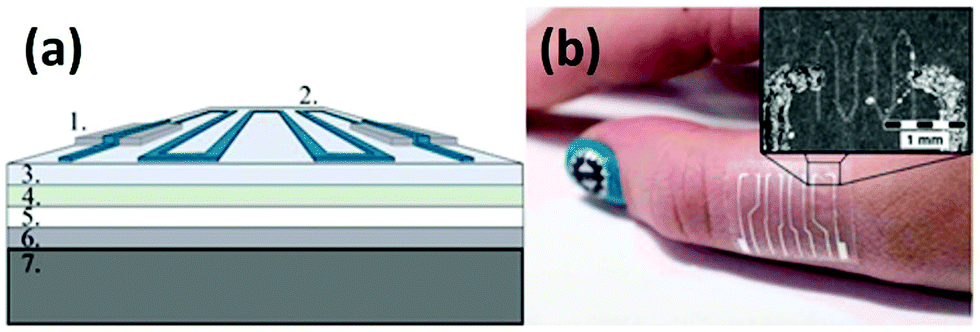 | ||
| Fig. 5 (a) Structural schematic of an inkjet-printed GRPP-based temperature sensor. (1) Screen-printed Ag conductors, (2) wave-patterned GRPP temperature-sensing element, (3) PU surface layer, (4) adhesive layer, (5) protective paper, (6) PET film, and (7) cooling/heating element. (b) A photograph of the GRPP-based temperature sensor, which contains four parallel sensors to constitute a sensor array, being attached to the skin. Reproduced from ref. 118 with permission. Copyright 2018, Nature Publishing Group. | ||
By integrating with other functional components and necessary accessories, 2DLNs-based temperature sensors can be used for developing some advanced WBEDs capable of realizing more complicated biomedical managements, such as precise human motion monitoring. Wang and Hou's group introduced an all graphene-based device that can sense human body touch through detecting body temperature based upon thermoelectric effects of graphene.119 According to this unique sensing principle, an all-graphene sensor pad can enable human touch locating and pressure level measuring under zero working voltage.
Boland and coworkers presented their research on the influence of adding graphene to a lightly cross-linked commercial silicone polymer, Silly Putty (Crayola, Easton, PA), which is a highly viscoelastic material under ambient conditions.125 In this study, graphene was prepared by LE of graphite in N-methyl-pyrrolidone, followed by being transferred into chloroform and mixed with Silly Putty directly. The obtained graphene and Silly Putty composite (G-putty) achieved excellent conductivity and stiffness from graphene, and meanwhile still retained the viscoelastic characteristics of Silly Putty. Due to the low matrix viscosity in this composite, graphene nanosheets in G-putty can shift and respond to deformation, therefore composing a mobile network, which can break and reform during mechanical deformation in a time-dependent manner. The possibility of measuring pulse rate, respiration rate, and joint motion using G-putty was tested and it achieved an unprecedented sensitivity. With further calibration, the peak-to-peak amplitude of the waveform was converted to pulse pressure, and a normal value of ∼40 mmHg for human body can be successfully determined.
Yao and coworkers reported a fractured microstructure design to conductive sponges, which was used for fabrication of a flexible and low-cost piezoresistive pressure sensor. GO synthesized by a modified Hummers method was dip-coated on commercial PU sponges.123 Through a multi-step procedure including acid activation, hydrothermal reduction, and compression treatment, fractured rGO wrapped PU sponges (rGO–PUS) were obtained. Its piezoresistive sensing mechanism is based on resistivity change of this conductive sponge caused by variation of the contact among conductive nanofibers during compressive deformation. The sensitivity of pressure sensors was significantly enhanced due to the unique structural design, and its cycling stability was high as reflected by repeatable and reproducible output of signals over 10000 cycles’ tests without detectable performance degradation. These advantages make rGO–PUS a promising material for manufacturing low-cost artificial skin.
Wu et al. reported the first experimental study of the piezoelectric properties of 2D MoS2.126 A monolayer MoS2 flake was produced by ME (Fig. 6a) and further prepared into a flexible mechanical sensor (Fig. 6b). The results showed that cyclic stretching and releasing MoS2 flakes with an odd number of atomic layers can produce piezoelectric voltage and current signals, whereas no signal is observed for flakes with an even number of layers and bulk MoS2 with a thickness more than 100 nm (Fig. 6c). For odd-layer samples, their piezoelectric output is large and decreases roughly as the inverse of layer number. These results confirm that monolayer MoS2 with broken inversion symmetry has a strong intrinsic piezoelectric response, whereas centrosymmetric bilayers and bulk MoS2 crystals are non-piezoelectric.127 The superior piezoelectric feature as well as large mechanical flexibility/stretchability of monolayer MoS2 demonstrates its great potential in wearable mechanical sensing applications.
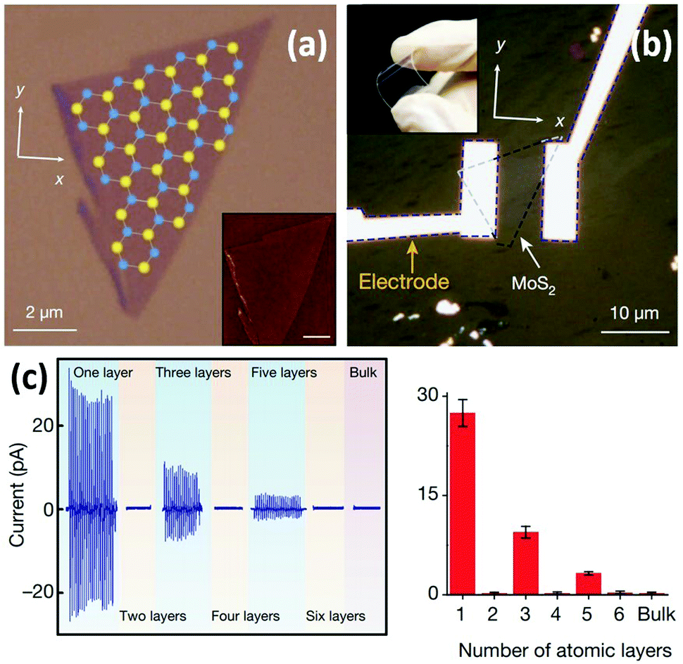 | ||
| Fig. 6 A monolayer MoS2-based flexible piezoelectric mechanical sensor. (a) An optical image of the monolayer MoS2 flake with superimposed lattice orientation derived from second-harmonic generation results. Inset: An atomic force microscopy (AFM) image of a MoS2 flake. (b) An optical image of the monolayer MoS2-based flexible sensor with electrodes at the zigzag edges of the MoS2 flake. Inset: A photograph exhibiting its flexibility. (c) Variations of piezoelectric signals with increasing number of atomic layers in MoS2 flakes. For each device, mean values from 20 technical replicates are indicated. Error bars represent standard deviation. Reproduced from ref. 126 with permission. Copyright 2018, Nature Publishing Group. | ||
More recently, Feng and coworkers reported large-scale growth of 2D In2Se3 nanosheets by a templated CVD method, and further fabricated a 2D In2Se3 nanosheet-based wearable piezoresistive strain sensor array using a simple mask process (Fig. 7a).128 The as-fabricated strain sensor array contained 5 × 5 sensing units (or sub-sensors) with well-patterned spacings and channels (Fig. 7b), and was attached to the back of a finger joint with a model showing the position of each sub-sensor further constructed (Fig. 7c). The five sub-sensors along the middle of the array (marked as A, B, C, D, and E in Fig. 7c–e) showed high sensitivity to the uniaxial strain variation induced by finger bending, demonstrating the high applicability of this 2D In2Se3 nanosheet-based wearable piezoresistive strain sensor array in electronic skins (E-skins) for motion monitoring.
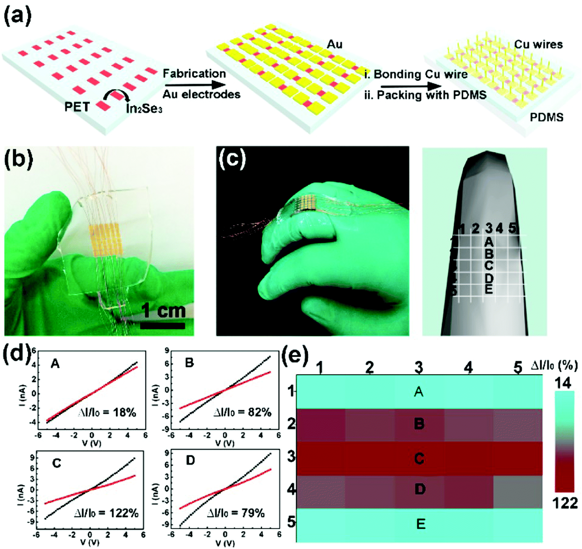 | ||
| Fig. 7 A 2D In2Se3 nanosheet-based strain sensor array and its spatial resolution test. (a) Schematic of the fabrication process of the In2Se3 thin film flexible strain sensor array. (b) A photograph of the strain sensor array (containing 5 × 5 sub-sensors) based on a patterned In2Se3 thin film. The channel length and width are 0.5 and 1.9 mm respectively, with 0.5 mm device spacing. (c) A photograph (left) and a 3D model (right) of the strain sensor array attached onto a middle finger to show positions of A, B, C, D and E sub-sensors. (d) I–V curves measured from the corresponding devices. (e) Spatial distribution of relative current changes in the strain sensor array during finger bending. Reproduced from ref. 128 with permission. Copyright 2018, American Chemical Society. | ||
Many efforts have been devoted to fabricating 2DLN-derived 3D aerogels owing to their elastic and piezoresistive properties. For example, 2D graphene nanosheets assembled 3D aerogels can show sensitive resistive responses to applied pressures (Fig. 8).107 The chemically converted graphene aerogel (CCGA) is connected with a lamp and a battery to form a simple circuit (Fig. 8a). The lamp gradually become brighter/darker, indicating resistance changes of the CCGA under increased/decreased compressive strain. Resistance of the CCGA in the longitudinal direction decreased from 69.4 (original state) to 6.6 Ω (90% of maximum strain), exhibiting the high sensitivity of CCGA under compressive strain (Fig. 8b). The CCGA was quite durable under repeated compressing/releasing at 50% strain without obvious sensitivity degradation (Fig. 8c). The advantages of having such an elastic structure was further demonstrated in Fig. 8d–h, in which insoles containing a group of such 3D graphene assemblies can realize walking monitoring. The resistance of each graphene aerogel varied sequentially with the footsteps on/off the insole (Fig. 8g). Note that when a 70 kg man stepped on the insole, the pressure applied on the aerogel could reach about 70 kPa, exceeding operation ranges (i.e., the maximum compressive strength) of most current 2D nanomaterial based wearable mechanical sensors. This graphene-assembled sensor could accurately sense the whole movements of different parts of feet (Fig. 8h), so that it offers new opportunities for human whole movement monitoring.
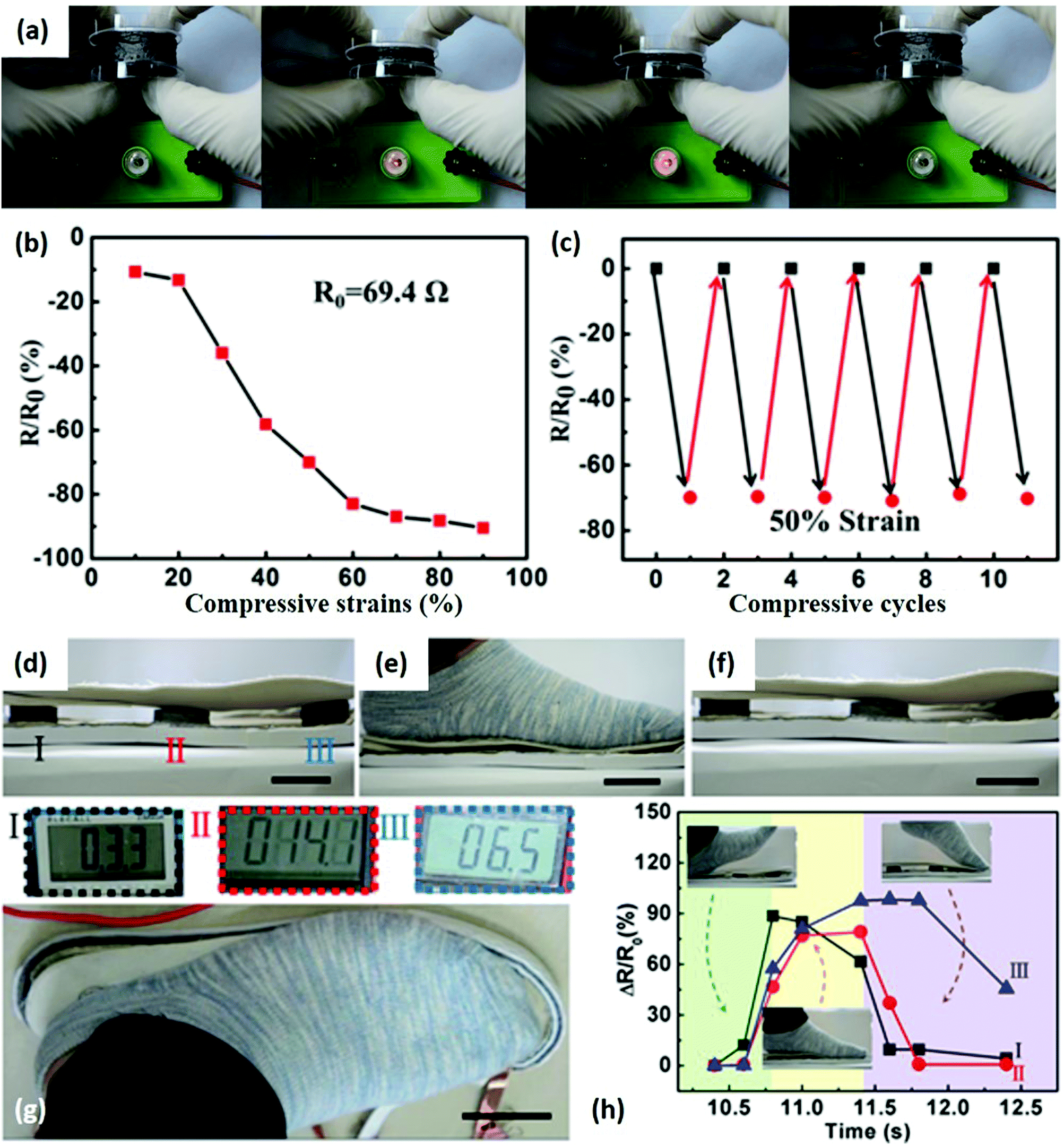 | ||
| Fig. 8 A CCGA-based step sensor. (a) Photographs illustrating resistance changes of a CCGA under compressive strain. Higher compressive strain led to a brighter lamp in the circuit. (b) Resistance of CCGA as the function of applied compressive strain. (c) Resistance changes under repeated compressive strain at a strain of 50%. (d–f) CCGAs sandwiched in insoles were compressed and released when a foot moved on and off the insole. (g) The resistances of CCGAs were measured by a multimeter. (h) The resistance variations of each graphene aerogel measured in one footstep during walking. Scale bars: 4 cm. Reproduced from ref. 107 with permission. Copyright 2018, Elsevier. | ||
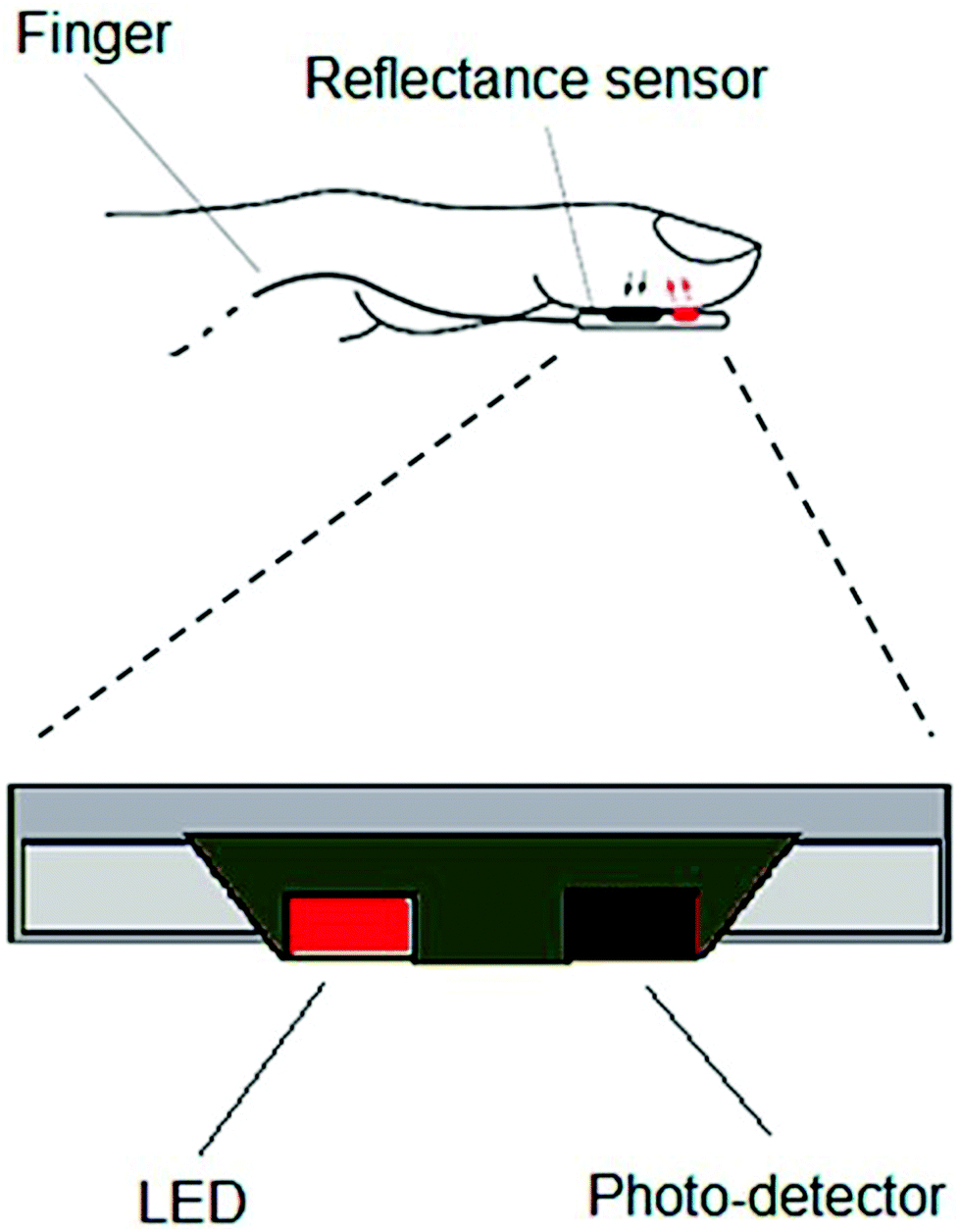 | ||
| Fig. 9 Schematic of a typical optoelectronic sensor for pulse rate measurement. Reproduced from ref. 129 with permission. Copyright, 2018 MDPI. | ||
2DLNs possess many remarkable properties such as strong light–matter interactions, extremely high charge carrier mobility, excellent intrinsic flexibility, high mechanical strength, good thermal conductivity, and ease of scalable processing, which can afford great promise towards the development of high-performance 2DLNs-based flexible photodetectors.130 For example, owing to its zero band gap and semi-metallic nature, graphene can interact with light over a wide spectral range from terahertz (THz) to UV wavelengths, thereby making it suitable for developing various broadband photodetectors.130 Although low light absorption and short exciton lifetime of graphene lead to low responsivity of graphene-based photodetectors, this could be effectively improved by suitable material functionalization, adopting special device structure, and developing graphene-based heterostructures.131 Furthermore, other 2DLN semiconductors with direct or indirect band gaps such as MoS2 and phosphorene possess not only quite high charge carrier mobility, but also high on/off ratio, showing a great potential in logic switching devices for diverse electronic applications.131 Compared with broadband photoresponse of graphene, MoS2 and phosphorene could bring a more selective and sensitive photoresponse, which could be quite significant for wearable biomedical applications.131 Electronic/optoelectronic properties of 2DLN semiconductor materials are strongly dependent on material structural symmetry and thickness.126,131 Thus, by carefully choosing suitable 2DLN semiconductor materials and controlling their thickness, optimized responsivity and fast response speed can be achieved with corresponding photodetectors.131 Main working mechanisms of 2DLNs based photodetectors include photoconductive effects, photogating effects, photovoltaic effects, photothermoelectric effects, and bolometric effects.132 These mechanisms have already been introduced in several previous papers and are thus not detailed here.130–132
Zheng et al. fabricated a flexible, transparent, highly stable and ultra-broadband photodetector based on 2D centimeter-scale and high-crystalline WSe2 films that can be synthesized by PLD on flexible and transparent polyimide (PI) substrates.133 Indium tin oxide (ITO) was further deposited by PLD on the substrate to provide the device conductivity. The obtained WSe2-based photodetector exhibits average transparency of 72% in the visible range and superior photoresponsive characteristics, such as an ultra-broadband detection window from 370 to 1064 nm, a very high external quantum efficiency up to 180%, a high reversible responsivity of 0.92 A W−1, and a fast response time of 0.9 s. These excellent optoelectronic properties as well as outstanding mechanical flexibility and stability in air make the WSe2-based photodetector very promising for wearable optoelectronic sensing applications. Song et al. presented a scalable solvothermal method to produce vdW heterostructures consisting of TMCs and graphene.134 A macroscale freestanding heterostructured thin film with excellent mechanical flexibility was fabricated by simply filtering a Bi2Se1.5Te1.5 and graphene nanocomposite (BSTG). The photoresponse of this BSTG-based flexible device under visible/infrared light emitting and 532 nm laser illumination at different laser powers was systematically evaluated. The result showed that the photocurrent could be effectively turned on and off and tuned by different laser powers. The flexible photodetector showed a broadband photoresponse and excellent durability in a bending test, demonstrating its potential for flexible optoelectronic devices. Song et al. reported the fabrication method of 2D solution-processed monolayer CsPbBr3 nanosheets and its application in high-performance flexible photodetectors.104 This 2D CsPbBr3 nanosheet-based photodetector exhibited strong responsivity at 517 nm and possessed a great potential to be used for green light detection.
Photodetectors can also be used for monitoring environmental light radiation. UV exposure can help our body produce vitamin D. However, it is also widely recognized as a major environmental risk factor for various skin diseases.135 Realizing real-time determination of UV exposure can help optimize our vitamin D uptake and effectively lower the risk of skin diseases. Wang and coworkers successfully synthesized large-scale 2D Pb1−xSnxSe nanoplates with a thickness of 15–45 nm on mica sheets by vdW epitaxy (vdWE), a kind of CVD method.136 The 2D Pb1−xSnxSe nanoplates are triangle or square with smooth surface (Fig. 10a). The nanoplate thickness was highly dependent on source and substrate temperature during synthesis. Under an optimal condition, the thickness of a square nanoplate was measured to be 21 nm by AFM (Fig. 10b). The 2D Pb1−xSnxSe nanoplates-based flexible optoelectronic device was fabricated in situ (Fig. 10c). Further results showed that the photodetector exhibited a broad spectral detection range from UV to infrared light with fast, reversible and stable responsivity at 800 nm (Fig. 10d). Sun et al. developed a universal molecular self-assembly approach to the synthesis of ultrathin 2D TMOs nanosheets (including TiO2, ZnO, WO3, and Co3O4) by rationally employing lamellar reverse micelles.45 Flexible photodetectors based on these TMOs were prepared, and their photoresponsive behaviors under 325 nm UV emission was investigated. Results showed that the time-dependent responses of these devices are highly stable and reproducible, and no degradation was found. These findings show a great potential of utilizing these 2D TMOs for practical UV sensing.
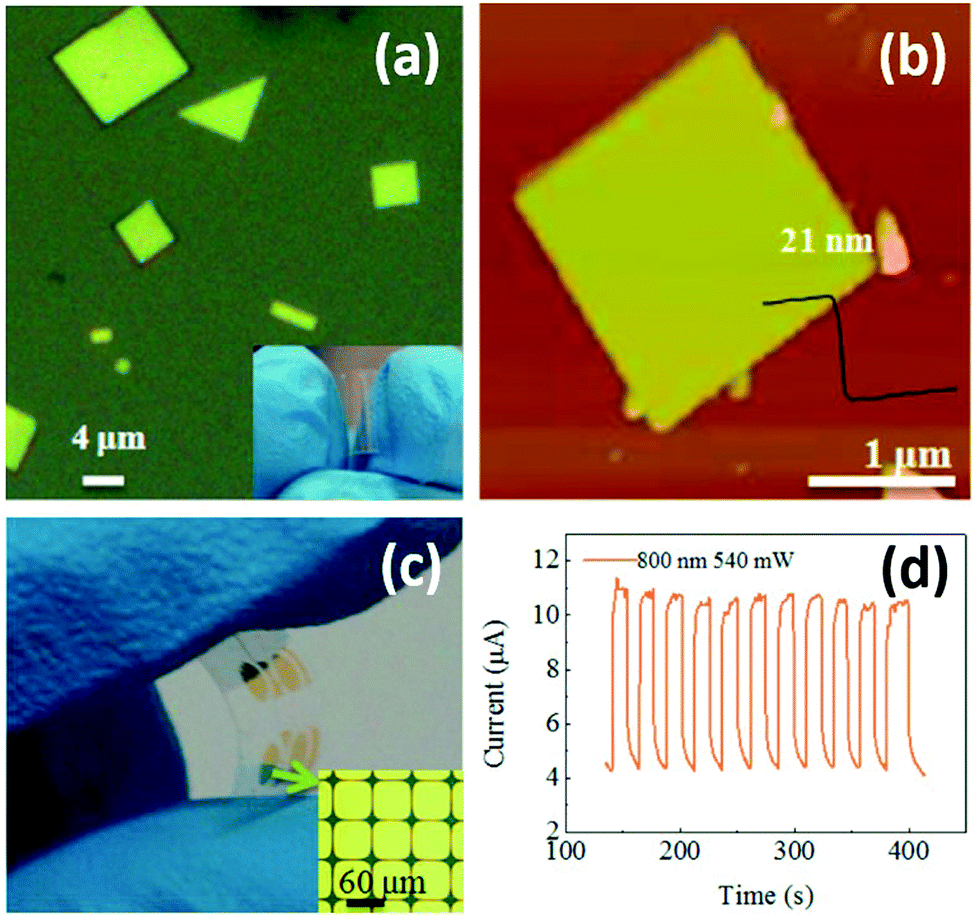 | ||
| Fig. 10 2D Pb1−xSnxSe nanoplates synthesized by vdWE and their application in flexible optoelectronic devices. (a) An optical image of 2D Pb1−xSnxSe nanoplates. Inset: An optical image of a flexible mica sheet. (b) A typical AFM image of a single 2D Pb1−xSnxSe nanoplate. (c) An optical image of the 2D Pb1−xSnxSe nanoplates-based flexible optoelectronic device. Inset: An optical image of the electrode pattern. (d) Time-dependent photoresponse of the 2D Pb1−xSnxSe nanoplates-based device under a laser beam of 800 nm wavelength and 540 mW light power at a bias of 2 V. Reproduced from ref. 136 with permission. Copyright 2018, American Chemical Society. | ||
 | ||
| Fig. 11 Graphene-based flexible electrodes for dynamic ECG monitoring. (a) Schematic of a graphene-based flexible electrode. (b and c) Photographs of a graphene-based flexible electrode and a GP. (d) An assembled electrode. (e) Schematic of the graphene textile. (f and g) Photographs of a graphene textile electrode. (h) Comparison of ECGs recorded by the graphene textile electrode when the patient was seated and resting, walking, swinging arms, and after exercise. Reproduced from ref. 139 with permission. Copyright 2018, MDPI. | ||
Borini et al. reported a graphene-based flexible humidity sensor, which showed an unprecedented response speed (∼30 ms response and recovery times) to a modulated humid airflow with an optimal film thickness by impedance analysis, owing to the 2D nature of GO and its super permeability to water.145 Based on this fast response humidity sensor, a ‘whistling’ recognition analysis was demonstrated, indicating the sensor has opened a door to various applications, such as touchless user interfaces. Yasaei et al. explored the humidity sensing performance of LE-produced phosphorene nanosheets (PNSs) and observed an ultrasensitive and selective signal response toward humid air with a very minor drift over time (Fig. 12a).144 Free-standing stacked PNSs-based films were further prepared by vacuum filtration and used to fabricate a humidity sensor. Drain current of the PNSs-based humidity sensor increased by ∼4 orders of magnitude as the relative humidity (RH) varied in the range of 10% to 85%, which indicates that the sensor possessed very high sensitivity (Fig. 12b). A stability test revealed that response of the BP film sensors remained nearly unchanged after exposure to ambient conditions for 3 months.
 | ||
| Fig. 12 A PNSs-based flexible sensor for humidity sensing. (a) Signal responses of stacked PNSs to different analytes. The left inset shows a typical sensor fabricated on a flexible polytetrafluoroethylene film that was attached onto a scotch tape for mechanical support and Ga–In eutectic contact. The right inset magnifies the same curves. (b) Current values of the sensor vs. RH at 25 °C. The inset shows a schematic of the custom-made chamber used for the experiment. Reproduced from ref. 144 with permission. Copyright 2018, American Chemical Society. | ||
Surface acoustic wave (SAW) devices are a kind of very important building blocks for electronics, which have been widely used for humidity monitoring due to their high sensitivity, small size, and ability to be interfaced with wireless communication systems. Xuan et al. reported a flexible SAW-based RH sensor.146 The sensor was fabricated on a PI substrate (Fig. 13a) with GO used as a sensing layer due to its large surface area and excellent hydrophilicity. With increasing humidity, the absorbed water molecules by the GO layer would accumulate, inducing a mass loading effect, leading to the resonant frequency shifting. The sensor had two resonant peaks (A0 and S0 Lamb wave modes) with large amplitudes (Fig. 13b), further exhibiting high sensitivity up to 145.83 ppm %RH−1 and fast response of only 4.4 (from 80% to 10% RH) and 25 s (from 10% to 80% RH) (Fig. 13c). The device also displayed great flexibility and stability, therefore holding great potential for wearable humidity sensing applications.
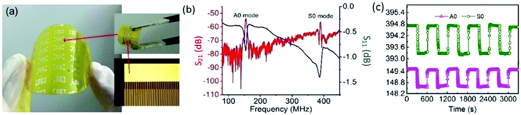 | ||
| Fig. 13 A flexible SAW-based RH sensor with GO as the sensing layer. (a) A photograph of the flexible humidity sensor fabricated on PI substrate with the enlarged part showing interdigitated transducers. (b) The transmission spectrum (S21, red) and the reflection spectrum (S11, blue) of the device with an acoustic wavelength of 12 μm. (c) Repeatability and response of the sensor for humidity changing between 80% and 10% RH. Reproduced from ref. 146 with permission. Copyright 2018, Elsevier. | ||
3.2. Two-dimensional layered nanomaterials supported wearable biomedical sensors for chemical/biological signal sensing
Under the quick pace of modern life, people hope to obtain their daily health information and routine diagnosis results simpler, faster, and timely. Making appointments with clinics frequently, lining up for visiting doctors or waiting for the examination of large medical equipment can be very time-consuming and vexatious, and should be reduced or avoided as much as possible. The rapid development of wearable chemical/biological sensor technologies could help us to achieve such a goal through continuous POC monitoring of major biomarkers in body fluid or exocrine secretion, based on a series of electrochemical, biochemical, or optoelectronic signal recognition processes. Combined with some other functional components such as real-time actuation units for treatment (e.g., drug release), this could also be a very feasible and convenient solution for diagnosis and therapy for many chronic or homeostasis-related diseases. Besides, wearable chemical/biological sensors are also very useful for monitoring indoor air quality and realizing real-time, dynamic and customized environmental control.Owing to their large specific surface areas, excellent electronic conductivity, high sensibility to surface chemical states and superior capabilities on optical/optoelectronic/electrochemical signal regulation, many 2DLNs have been employed for recognizing analytes (e.g., small biomolecules, ions, gas molecules, and bacteria) existing in solution or atmosphere with high sensitivity and selectivity.147 By integrating with enzymes or aptamers, constructing host–guest inclusion complexes, or utilizing synergistic effects of different functional materials, 2DLNs-supported wearable chemical/biological sensors could achieve even better sensing performances. Depending on specific designs of sensing processes, working mechanisms of different sensors could be varied greatly. In this section, distinguished by analyte locations, various 2DLNs-supported wearable chemical/biological sensors are described.
He et al. presented a novel type of flexible electrodes based on Pt–Au alloy nanoparticles (PtAuNPs) decorated free-standing rGO–CNT–ionic liquid (IL) loaded GPs, and explored their practical application in electrochemical nonenzymatic sensing of glucose in human blood samples.148 In this study, a GO and CNT mixture dispersion was hydrothermally-reduced to prepare a 3D ‘skin-skeleton’ structural rGO–CNT aerogel, which was further ground with IL to prepare a rGO–CNT–IL gel ink. Free-standing GPs were prepared by roll-printing a GO aqueous dispersion onto a piece of commercial printing paper, followed by hydroiodic acid reduction. The rGO–CNT–IL gel was dropped and roll-printed onto GPs, and then PtAuNPs were ultrasonic-electrodeposited onto the rGO–CNT–IL loaded GPs to obtain the final flexible nanohybrid electrodes (PtAuNPs@rGO–CNT–IL@GPs) (Fig. 14a). From Fig. 14b and c, highly dense PtAuNPs were observed to be uniformly grown into the 3D structure. Due to the synergistic contributions of different ingredients, the electrodes could exhibit excellent sensing performances to blood glucose (limit of detection (LOD): 8 μM) as well as superior mechanical properties (Fig. 14d). Therefore, these electrodes are very promising to be applied for next-generation wearable blood glucose testing devices. Liu and coworkers prepared flower-like 2D CuCo2O4 nanosheets anchored on commercial flexible graphite papers using a facile hydrothermal method followed by a post-annealing treatment.149 The as-prepared functional graphite papers could be used as electrodes for nonenzymatic glucose sensors with good sensitivity and selectivity, extraordinary linear response, and a low LOD of 5 μM. Moreover, these electrodes could also exhibit excellent supercapacitive properties (1131 F g−1 at 1 A g−1, superior high-rate performance and good long-term cycling stability), which showed great promise for functioning as a multifunctional platform used in WBEDs.
 | ||
| Fig. 14 PtAuNPs@rGO–CNT–IL@GPs as flexible electrodes for electrochemical non-enzymatic sensing of glucose in human blood samples. (a) The fabrication process of PtAuNPs@rGO–CNT–IL@GPs. (b and c) Scanning electron microscope (SEM) images of PtAuNPs@rGO–CNT–IL@GPs. Inset of (b): A photograph of the PtAuNPs@rGO–CNT–IL@GP. (d) Typical amperometric response of PtAuNPs@rGO–CNT–IL@GP electrode to successive additions of 0.1, 0.2, and 0.5 mM glucose in stirring phosphate-buffered saline (pH 7.4) at an applied potential of +0.2 V. Inset of (d): The corresponding calibration curves. Reproduced from ref. 149 with permission. Copyright 2018, Elsevier. | ||
Lactate is an important biomarker for a variety of diseases, such as heart failure, drug toxicity, and metabolic disorders. Labroo and Cui developed a flexible graphene-based enzymatic biosensor to detect lactate.150 A biosensor was fabricated by transferring CVD synthesized graphene onto a flexible PET substrate, followed by immobilizing a bioreceptor on graphene nanosheets (Fig. 15a and b). The sensor exhibited a high detection sensitivity from 0.08 to 20 μmol L−1 with a fast steady state measuring time of 2 s (Fig. 15c), and was still able to rapidly detect low concentrations of lactate sensitively under different mechanical conditions.
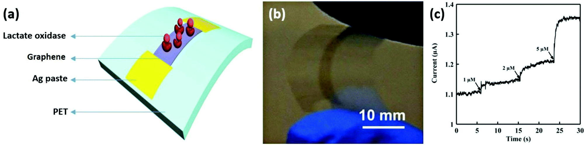 | ||
| Fig. 15 A flexible graphene-based enzymatic biosensor for lactate detection. (a) Schematic of lactase oxidase functionalized graphene attached on a flexible PET substrate. (b) A photograph of the biosensor. (c) A current–time curve of the lactate sensor to 1 μM, 2 μM, and 5 μM of lactate. Reproduced from ref. 150 with permission. Copyright 2018, Elsevier. | ||
Dopamine (DA) is extensively distributed in the mammalian central nerve system and plays a significant role in metabolism and nervous activity. Ng et al. presented the fabrication of a flexible rGO-based microelectrode array (MEA) using a modified nanoimprint lithography (NIL) technique for DA sensing.151 GO synthesized by a modified Hummers’ method was first spin-coated onto a conductive ITO layer modified flexible PET film (ITO–PET). Then, electrochemical reduction was conducted, followed by a NIL process to obtain the final rGO-based MEA. The as-prepared MEA exhibited very high SNR in sensing DA, as well as simultaneously sensing tyrosine and H2O2. Sensitivity was almost unaffected under a continuous flow condition when the rGO-based MEA was incorporated into a microfluidic device. Furthermore, the sensor showed good wearability due to its remarkable mechanical stability. Zan and coworkers reported the construction of a novel nanohybrid electrode by structurally integrating 2D assembled dendritic Pt nanoparticles (PtNPs) on flexible GPs, which shows superior performance in detecting DA released from living cells (LOD: 5 nM).152
H2O2 is a resultant or intermediate of numerous biochemical reactions. Chi et al. explored Au nanoparticles (AuNPs) as a catalyst for preparing core–shell structured nanoparticles (Au@PBNPs) with AuNP core and Prussian blue (PB) shell, and used Au@PBNPs to functionalize GPs as advanced electrochemical H2O2 sensors.153 With the doping of Au@PBNPs, conductive, flexible, and free-standing composite GPs can be easily fabricated by vacuum filtration. The composite electrode exhibited high performance in electrocatalytic H2O2 reduction. A synergistic interaction between Au@PBNPs and graphene supports may play a key role in enhancing H2O2 sensing performances. With a similar approach, nanohybrid paper electrodes consisting of rGO nanosheets and PB nanoparticles were fabricated, which also exhibited superior capabilities towards H2O2 and enzymatic glucose detection.154
Mailly-Giacchetti et al. reported the fabrication of a graphene-based solution-gated FET on a flexible poly(ethylene 2,6-naphthalenedicarboxylate) substrate for pH sensing.155 The FET pH sensor was capable of exhibiting a high sensitivity of 22 mV pH−1. Moreover, the study showed that both the use of a flexible substrate and the presence of moderate amounts of organic residues attached to graphene would not significantly influence electrical signal responses of the sensor to pH variation, which would simplify large-scale fabrication of the graphene-based pH sensor.
Lee et al. reported a new class of graphene-based diabetes monitoring/therapy devices.5 In conjunction with a sweat-control layer, the flexible skin-mounted graphene-hybrid sensing array was capable of sweat-based glucose sensing. By rational transforming, precisely measured sweat glucose concentrations could be used for estimating blood glucose levels. Ancillary functions including RH, pH, tremor, and temperature sensing could give assistance to correct measured values of sweat glucose concentration and regulate transcutaneous drug delivery. In addition, connections of the graphene-hybrid wearable sensor to a portable/wireless power supply and a data transmission unit would enable POC treatments of diabetes.
Kinnamon et al. demonstrated a portable biosensor for detecting a typical stress biomarker, cortisol, in human sweat.156 LE-processed MoS2 nanosheets were loaded onto flexible nanoporous polyamide substrates and surface functionalized with cortisol antibodies towards developing an affinity biosensor specific to the physiological relevant range of cortisol in perspired human sweat. MoS2 nanosheets could offer large surface areas and abundant binding sites for antibody loading. Their semi-conducting nature and appropriate direct band gap could also help achieve better sensitivity. Cortisol sensing was performed by measuring impedance changes associated with cortisol binding along the MoS2 nanosheets. High sensitivity (1 ng mL−1) and specificity were achieved by this method.
Liao et al. proposed a flexible organic electrochemical transistor-based sensor for uric acid (UA) detection.157 The Pt gate electrodes were modified with a polyaniline (PANI) and Nafion–graphene bilayer film that could effectively block the interference from charged biomolecules. Graphene was used for improving electrocatalytic activity and conductivity of the gate electrode. Uricase (UOx) was immobilized onto the surface of PANI, and the functional groups of GO could readily react with amine groups of UOx and reactive moieties of the conductive PANI layer, resulting in optimized enzyme immobilization. The UA sensor demonstrated good selectivity and a LOD of 10 nM, and the proposed strategy was also successfully applied for cholesterol and glucose detection.
Jiang et al. prepared a free-standing sulfonic acid functionalized GO (fSGO) based electrolyte film, which was used as an alcohol fuel cell sensor for the detection of alcohol vapor, whose value could be further used for estimating blood alcohol content.158 Due to the high proton conductivity of fSGO, the sensor could detect ethanol vapor with excellent sensitivity (25 ppm) and selectivity. These results exhibit a promising application potential of fSGO films in a wearable breathalyzer.
Yun et al. demonstrated a bendable and washable electronic textile NO2 gas sensor composed of commercially available yarn and rGO.159 The gas sensor possessed several remarkable features including chemical durability, mechanical stability, and ultrahigh sensitivity (0.1 ppm) at room temperature, which might due to the robust rGO wrapping on the yarn surface and the large accessible surface area of the rGO-functionalized yarn.
Sayed et al. fabricated a high-performance CO gas sensor based on laser-reduced rGO deposited on flexible PET substrates.160 The CO gas sensor was comprised of four interconnected rGO strips in a Wheatstone bridge verification circuit. Physically adsorbed CO molecules on rGO could induce resistivity decrease of rGO, wherein CO molecules acted as electron donors. At 100 ppm of CO, the sensor could exhibit an average response and recovery time of 70 and 40 s at room temperature.
Utilizing an inkjet-printing technique, Seekaew et al. fabricated a novel flexible NH3 gas sensor made of GRPP films with high uniformity over a large area (Fig. 16).161 The gas sensor exhibited high response and selectivity to NH3 in a low concentration range of 25–1000 ppm at room temperature. The excellent signal response is attributed to increased specific surface area by graphene and enhanced interactions between the sensing film and NH3 molecules via π electron networking.
 | ||
| Fig. 16 Schematic of the fabrication process of a flexible NH3 gas sensor based on GRPP films. Reproduced from ref. 161 with permission. Copyright 2018, Elsevier. | ||
Cho et al. described a poly(styrenesulfonate) (PSS) doped PANI and graphene nanocomposite (PSPA@G) and its application in H2S detection.162 PSPA@G exhibited good compatibility with PET substrates, thus making it suitable for constructing flexible electrodes. Due to the strong π–π stacking interaction between PANI and graphene, charge transport in the fabricated electrode was greatly improved; therefore, an ultrahigh sensitivity for H2S detection was achieved (LOD: 1 ppm).
Toluene is known as a neurotoxic volatile organic compound (VOC) that can cause sick building syndrome.163 Choi et al. developed a highly sensitive, transparent and flexible toluene sensor by depositing sensing material Co-metalloporphyrin functionalized graphene on PET substrates.164 The sensor was successfully applied for detection of 10 ppm toluene at room temperature, and further exhibited optical transparency, mechanical flexibility, and high responsiveness by combining the excellent mechanical and electrical properties of graphene and catalytic activity of Co-metalloporphyrin.
Effective pathogen detection is necessary for the repression of microbial foodborne diseases, microbial infection, and other infectious diseases. Basu et al. fabricated a low-cost graphene-based Escherichia coli (E. coli) sensor.165 Graphene was deposited on Cu foil by CVD, and subsequently transferred onto a flexible acetate substrate to fabricate an E. coli sensor (Fig. 17a and b). Impedance analysis was conducted to characterize impedance variation as a function of E. coli concentration on the graphene's surface. The residual methyl groups of graphene acted as active binding sites for E. coli. With increasing E. coli concentration, the resistance of graphene decreased owing to the increased hole doping induced by negatively charged E. coli (Fig. 17c). The sensor could detect E. coli down to a clinically relevant concentration of ca. 106 cfu mL−1 (defined as colony-forming unit per milliliter). Mannoor et al. described a silk bioresorption approach to interfacing passive and wireless graphene nanosensors onto tooth enamel.166 By the self-assembly of antimicrobial peptides onto graphene, even single-cell levels of bacteria detection can be achieved remotely and bio-selectively. This highly sensitive and selective sensor may play a vital role in the defense against pathogenic threats at the point of contamination.
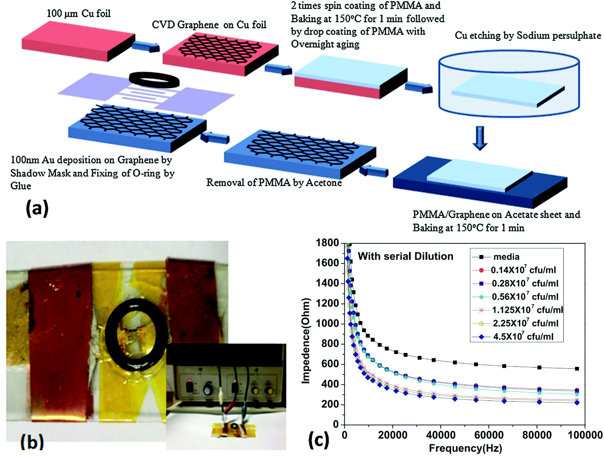 | ||
| Fig. 17 The graphene-based E. coli sensor. (a) Schematic of the fabrication process. (b) A photograph of the sensor. (c) Impedance versus frequency plots with different concentrations of E. coli. Reproduced from ref. 165 with permission. Copyright 2018, Elsevier. | ||
3.3. Two-dimensional layered nanomaterials supported auxiliary functions for wearable biomedical sensors
With the rapid expansion of WBED function menus, more and more original data and software will be integrated into WBEDs, which means high-performance local memories are strongly required. Son et al. reported large-scale WCS of MoS2 nanosheets and their wafer-scale integration for producing a flexible resistive random access memory array.167 The excellent uniformity of the MoS2 array allowed large-area integration of pressure sensors and quantum dot (QD) LEDs to construct a flexible data storage and display system. Zhao et al. developed a facile, low cost, all-solution-processible method to prepare flexible and rewritable nonvolatile memory devices based on rationally assembled GCN as an insulator layer and direct laser writing graphene as electrodes.168 The as-prepared memory device showed non-volatile electrical bi-stability and rewritable memory effect with a reliable on/off ratio of up to 105.An amplifier can gather weak electric or bioelectric signals and increase their amplitudes for further processing, recording, or displaying. It could be integrated with a sensor electrode or just function as a relatively independent component. Zhu et al. reported a flexible PNSs-based FET.169 Based on its ambipolar functionality and high mobility, inverting and noninverting analog amplifiers with a voltage gain of ∼8.7 could be achieved more than two times higher than those of previously reported flexible thin film amplifiers.
A radio frequency (RF) front-end is a basic building block in most wearable wireless communication systems that can send and receive RF signals for data communication. Huang et al. fabricated a RF front-end with printed graphene enabled transmission lines and antennas on a conventional paper substrate.170 Further results showed that bending and twisting the transmission lines did not alter transmission coefficients much, which are highly desirable for wearable applications (Fig. 18a). When the distance between the two antennas was 0.5 m, the transmission coefficient from 1.67 GHz to 2.87 GHz was above −32 dB, which was more than 20 dB higher than −55 dB observed out of bands above 3.8 GHz (Fig. 18b and c). These results verified that RF signals could be effectively radiated and received by these two graphene antennas. Combined with its low cost and environmental friendliness, the RF front-end is very promising to be used in future wearable wireless communication systems.
 | ||
| Fig. 18 A printed graphene enabled RF front-end for RF signal transmitting. (a) Un-bended (1), bended (2) and twisted (3 and 4) transmission lines and their transmission performances. (b) The transmission measurement setting between two printed graphene enabled wearable antennas on a mannequin. (c) The transmission measurement between the two antennas with 0.5 m separation. Reproduced from ref. 170 with permission. Copyright 2018, Nature Publishing Group. | ||
As introduced earlier, transducers are essential components in chemo-/biosensors since they can convert hard-to-handle chemical/biological signals into other simplified measurable signals.171 Kwon et al. proposed a controlled synthetic method for the large-scale fabrication of graphene micropatterns, which were used as high-performance transducers in FET-type flexible fluidic human immunodeficiency virus (HIV) immunoassays.172 Benefitting from superior synergistic effects between signal recognition elements and the high-performance graphene micropattern transducers, the as-fabricated immunosensors could achieve a LOD of 1 pM to HIV-2 Ab (a specific biomarker), which indicated its excellent sensitivity.
Withers et al. fabricated a series of high-performance LEDs for wearable flexible displays using graphene as transparent conductive layers, h-BN as tunnel barriers, and different TMCs as quantum well materials.173 Combining different 2DLNs in these LEDs achieved fine-tuning of emission spectra and also an enhanced electroluminescence with a quantum yield of 5%. Therefore, these LEDs are very suitable for signal indicating in flexible and transparent electronics.
Electrochromic materials can vary their optical properties reversibly and persistently under an external voltage, which is very promising to be widely used in advanced WBEDs for energy-saving indications of various signal changes.174 By a facile electrodeposition process, Li et al. constructed a 3D quasi-vertical nanosheet architecture from self-assembling 2D WO3·2H2O nanosheets on flexible ITO–PETs.175 Enhanced electrochromic performances were achieved, including a high coloration efficiency of 52.6 cm2 C−1 and fast switching times of 17 and 3.8 s during coloration and bleaching. These could be caused by the well-defined layered structure of 2D WO3·2H2O nanosheets and the large active surface area of the obtained 3D self-assembly structure, which can shorten the diffusion pathway among electrode materials and give rise to high optical modulation capability and good cyclic stability.
Actuators can provide controllable mechanical responses when triggered by specific signal stimuli. Therefore, they can be applied in WBEDs for smart quantitative sampling and controlled transcutaneous drug delivery as well as other simple biomimetic motions.176,177 He et al. presented a novel strategy to fabricate moisture gradient responsive thin films based on a rGO and polydopamine composite.178 Driven by a water absorption induced moisture gradient, the uniform functional films could serve as highly efficient actuators.
Several kinds of 2DLNs can also be used as flexible and free-standing conductive substrates for sensor electrodes.139,148,154 In the fabrication of this kind of electrode, the use of adhesives and conductive agents can be exempted, which can save resources, reduce costs, and simplify production processes. Besides, these 2DLNs-based flexible and freestanding conductive substrates are extremely light, which can greatly lower the weight of whole electrodes. Furthermore, these 2DLNs-based flexible electrodes can exhibit enhanced structural stability and conductivity, due to a better binding between active materials and substrates.
4. Two-dimensional layered nanomaterials supported wearable power devices for biomedical applications
With the rapid popularity of WBEDs, performance bottlenecks derived from their power devices are tending to limit their further development. Executing multitasks simultaneously and handling big data have given higher requests to wearable power devices on their energy density, power density, reliability, and durability. Therefore, the significance of developing high-performance wearable power devices to meet increasing energy demands of WBEDs is becoming more evident and urgent. Moreover, different functional units are aiming to achieve tighter integration in WBEDs. High conformability of wearable power devices to both the human body and other functional units (especially wearable sensors) is highly expected, since it may bring significant impacts on sensing performances (e.g., sensitivity) as well as user comfortableness. Several kinds of wearable power devices for biomedical applications have been developed, such as batteries, SCs, PVs, BFCs, and NGs. Their basic structures and working mechanisms have been summarized by previous reviews.19,20,179,180 On one hand, these wearable power devices should meet typical requirements for common power devices, such as high energy or/and power density, good cyclic stability, rate performance, and high energy conversion efficiency. On the other hand, they should also possess good flexibility or/and stretchability for achieving better conformability and being capable of maintaining stable comprehensive performances even after repeated bending/stretching cycles. Superior physicochemical, electronic/optoelectronic, and mechanical properties of 2DLNs endow them with great potential to be widely utilized for improving current wearable power devices. In this section, multifold 2DLNs supported wearable power devices will be described, respectively.4.1. Two-dimensional layered nanomaterials supported flexible or/and stretchable batteries
For developing next-generation flexible or/and stretchable batteries, electrode active constituents with intrinsic flexibility or/and stretchability are favorable. Besides, current collectors, electrolytes, separators, and packing materials should also be as flexible/stretchable as possible to achieve a holistic structural configuration with high conformability. Until now, many types of flexible or/and stretchable batteries have been developed, such as LIBs, Na-ion batteries (SIBs), Li–S batteries (LSBs), and Zn–O2 batteries (ZOBs).19,181–183 2DLNs have been widely studied for their use as different battery components, such as electrode active constituents, solid electrolytes, current collectors and separators.Many 2DLNs- or 2DLNs-based composites can be fabricated into flexible and free-standing electrodes to effectively address issues related to the use of metal foil current collectors.19 These 2DLNs-based flexible current collectors or 2DLN composites-based free-standing electrodes are among the most attractive alternatives to conventional conductive agent and binder-based electrode designs, owing to their superior mechanical strength, excellent flexibility, high electric conductivity, and light weight. They could achieve improved corrosion/deformation tolerance and extremely high weight proportion of active materials, and their intrinsic flexibility is a vital factor for finally achieving full flexible batteries. Considering from the perspective of active materials, benefitting from their large specific surface area, reversible Li+ intercalation/extraction, fast intraplane electron transport, and superior structural stability, typical 2DLNs (e.g., graphene, phosphorene, Ti3C2) based anodes could offer much larger specific capacities than those of commonly used graphite-based anodes (2–10 folds), as well as better rate capability and cyclic stability.184 On the other hand, compositing suitable 2DLNs has becoming a major strategy for optimizing commercial pre-lithiated TMO (e.g., LiCoO2 (LCO), LiMn2O4 (LMO), LiFePO4 (LFP), and LiNixMnyCo1−x−yO2 (LNMCO)) cathode materials, since it can help greatly improve electric conductivity, microscopic mechanical strength, active material accessibility, and Li+ diffusion rate.185 Besides, large lateral size and solution processability of 2DLNs make them very suitable for large-scale printing production of flexible electrodes.
Li and coworkers prepared a paper-like graphene foam with a unique 3D macroscopic structure.186 High-quality CVD-grown graphene constituted a 3D interconnected network in the graphene foam, which could be used as fast transport channels of charge carriers. The graphene foam possessed many superior features, including excellent electrical and solid conductivity, ultralight weight, flexibility, high porosity, large specific surface area, and electrochemical stability. By using the graphene foam as an efficient current collector, thin, flexible, and ultralight LFP-loaded graphene foam anode (LFP@GF) and Li4Ti5O12 (LTO) loaded graphene foam cathode (LTO@GF) were prepared, respectively. An assembled full battery exhibited ultrathin thickness (<800 μm), high capacity (∼133 mA h g−1 at 1C (defined as the current to discharge the nominal capacity of a battery in 1 h)), good rate (∼117 mA h g−1 at 10C, recoverability of ∼88%), and cycling (10C, 100 cycles, retention of ∼96%) performances as well as excellent flexibility (Fig. 19). Both the fabrication of graphene foam and the active material loading process could be easily scaled up, which reflect a bright prospect of the large-scale application of this flexible battery for powering WBEDs.
 | ||
| Fig. 19 Characterization of the flexibility of a full battery based on LTO@GF and LFP@GF. (a) A photograph of the battery encapsulated by polydimethylsiloxane (PDMS) under bending, showing its good flexibility. (b) A photograph showing the battery was lighting a red LED under bending. (c) Galvanostatic charging/discharging curves of the battery. Red and blue lines represent the as-fabricated flat battery and the bent battery after repeatedly bending to a radius of 5 mm for 20 times, respectively. (d) Cyclic performances of the battery under flat and bent states. Reproduced from ref. 186 with permission. | ||
Cheng et al. developed a conductive gel system as an anode material, which comprised a continuously conductive LTO network based on cross-linking lithium titanate nanotubes hydrogels and GO colloids.187 The conductive gel system was further developed into inks compatible for various coating techniques. After coating, thermal annealing was employed for reducing GO to rGO. The rGO nanosheet-based highly conductive network, intrinsic high Li+ diffusion coefficient, short solid-state diffusion length, and LTO nanotubes based mesoporous structure could greatly promote ion transport, which is significant for developing LIBs with high-rate capability. A screen-printed on-chip full battery was further fabricated, which was composed of a LTO–rGO-based anode and a LFP–rGO-based cathode. The battery exhibited fast rechargeable capability, and its comprehensive performances could be further improved by optimizing material constituents and device structures.
In addition to being applied for constructing flexible electrodes, GO can be also used for developing highly efficient solid-state electrolytes. Using a polyethylene oxide (PEO) and GO-based flexible solid-state electrolyte film (PEOGOF), Kammoun and coworkers reported a stretchable spiral thin-film LIB that is capable of large out-of-plane deformation of 1300% while exhibiting simultaneous electrochemical functionality.188 The spiral LIB exhibited robust mechanical stretchability even after 9000 stretching cycles and an energy density of 4862 mW h cm−3 at ∼650% out-of-plane deformation could be achieved. This solid-state electrolyte-based structural design can also offer enhanced safety and stability compared to those conventional designs employing organic liquid based electrolytes.
LSBs possess some unique advantages, such as low cost due to the use of S, as well as high energy density and low material toxicity.192 Integrating 2DLNs into LSBs, especially LSB cathodes, could help overcome several significant shortcomings. First, some 2DLNs could provide abundant surface binding sites and large surface areas for incorporating and encapsulating polysulfide species, restraining irreversible capacity loss due to polysulfide dissolution. Second, 2DLN composite-based electrodes could possess better electric conductivity. Third, the introduction of 2DLNs could effectively restrict the volume change of S-loaded cathodes during charge/discharge. Cao et al. fabricated highly flexible and free-standing paper electrodes by a rGO and S composite (rGO–S) for flexible LSB cathodes.193 The crosslinked 3D porous network structures could accelerate electron/ion transport and suppress polysulfides dissolution. By using these rGO–S paper electrodes, flexible soft-packaged (Fig. 20a) and cable-type (Fig. 20b) LSBs were assembled respectively, which exhibited high initial capacities of 1187 and 1360 mA h g−1 at 0.1C, respectively (Fig. 20c and d). Moreover, both of them could keep their working normally under bending and exhibit only very slight differences with the corresponding LSBs working under flat states (Fig. 20e and f).
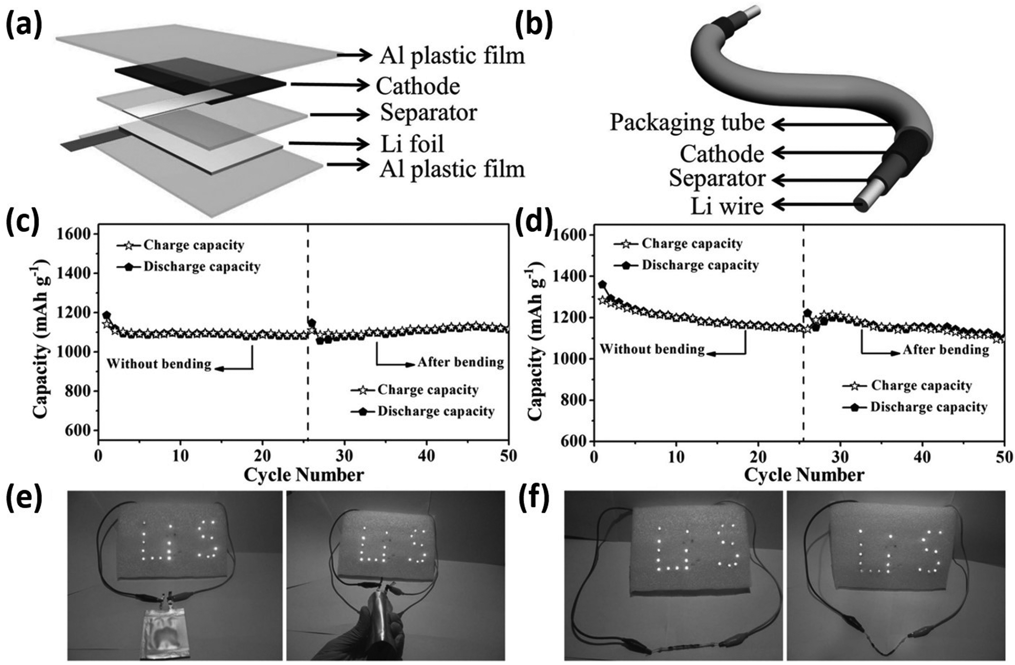 | ||
| Fig. 20 Two types of flexible LSBs based on the rGO–S paper electrodes. (a and b) Schematics of soft-packaged (a) and cable-type (b) LSBs. (c and d) Cycling performances of the soft-packaged (c) and cable-type (d) LSBs before and after bending. (e and f) A ‘LiS’-shaped string of lights containing 20 LEDs lit by soft-packaged (e) and cable-type (f) LSBs without bending (e and f, left) and under bending (e and f, right). Reproduced from ref. 193 with permission. Copyright 2018, John Wiley & Sons. | ||
ZOBs are receiving increased attention owing to their high theoretical energy density, low cost, and superior environmental friendliness.194 Although current rechargeable ZOBs still cannot provide sufficient cyclic stability and energy efficiency, many research labs are continuously working on improving existing ZOB techniques. One of the major focuses is to suppress the variation of electrolyte composition and volume due to an open cathode structure.194 Zhang et al. fabricated a functionalized nanocellulose and GO composite membrane (NCGOM) as an effective and practical hydroxide-conducting solid-state electrolyte for flexible and rechargeable ZOBs.195 An interconnected framework comprised of nanocellulose fibers was used to integrate GO into a flexible membrane with high water content. After crosslinking, the nanocellulose–GO composite membrane was endowed with high structural stability and water retentivity, as well as good adhesive ability to electrodes. A superior hydroxide conductivity of 58.8 mS cm−1 was achieved at 70 °C. Based on the functional membrane, a flexible full ZOB was fabricated, which exhibited superior rechargeability and performance stability.
All of the above findings show that 2DLNs are very powerful to be used for fabricating high-performance wearable batteries in WBEDs. Some typical 2DLNs-based flexible or/and stretchable batteries reported in recent years are summarized and compared in Table 2.
| Material | Battery type | Component | Energy density and rate performance | Cyclic stability |
|---|---|---|---|---|
| Note: CC-CoFe-LMH-NWA: carbon-coated Co–Fe layered double hydroxide nanowall array. TOB@ACF: TiO2(B) nanosheets anchored non-woven activated carbon fabric. rGOP: reduced graphene oxide paper. SiNW@G@rGOF: Si nanowire, overlapped graphene sheath and reduced graphene oxide overcoat sandwiched film. NGSP: N-doped graphene and SnO2 nanoparticle sandwiched paper. LTO@GF: three-dimensional graphene foam supported Li4Ti5O12 nanosheets. VACNT@rGOF: reduced graphene oxide film supported vertical aligned carbon nanotubes. MGCHP: MoS2, graphene and carbon nanotube hybrid paper. BP@GP: phosphorene and graphene hybrid paper. rGO@HBNF: reduced graphene oxide and hexagonal boron nitride composite film. GLFP: graphene and LiFePO4 nanocomposite. PEOGOF: polyethylene oxide- and graphene oxide-based flexible solid-state electrolyte film. MLIB: Mg–Li hybrid ion battery. S–CNT@G: S-loaded super-aligned carbon nanotube and graphene hybrid material. GCC@S + G-separator: S-coated graphene membrane cathode and graphene membrane coated commercial polymer separator. MSGCP: MoS2 and reduced graphene oxide composite paper. IQDs@rGOP: I quantum dots decorated reduced graphene oxide composite paper. GNP@GOP: graphene nanoplatelets loaded graphene oxide paper. LOB: Li–O2 battery. Co-LMH@CNS: Co(OH)2 and vertically aligned carbon nanosheet hybrid arrays. | ||||
| CC-CoFe-LMH-NWA196 | LIB | Anode | 1298 mA h cm−2 at 0.483 mA cm−2, no available data for rate performance | 60% capacity loss after 50 cycles at 0.483 mA cm−2 |
| TOB@ACF197 | LIB | Anode | 210 and 97 mA h g−1 at 2 and 30C | 13% capacity loss after 2000 cycles at 20C |
| rGOP198 | LIB | Anode | 150 and 70 mA h g−1 at 13.3 and 26.6C | No apparent capacity loss after 1000 cycles at 13.3 and 26.6C |
| SiNW@G@rGOF199 | LIB | Anode | 500 and 420 mA h g−1 at 8.4 and 12.6 A g−1 | 20% capacity loss after 100 cycles at 2.1 A g−1 |
| NGSP200 | LIB | Anode | 918 and 500 mA h g−1 at 0.1 and 5 A g−1 | No apparent capacity loss up to 100 cycles at 0.05 A g−1 |
| LTO@GF186 | LIB | Anode | 169 and 135 mA h g−1 at 1 and 200C | 4% capacity loss after 500 cycles at 30C and 100C |
| LTO–rGO187 | LIB | Anode | 175 and 125 mA h g−1 at 1C and 90C | 5% capacity loss after 1000 cycles at 90C |
| VACNT@rGOF201 | LIB | Anode | 265 and 55 mA h g−1 at 0.06 and 3.6 A g−1 | No apparent capacity loss after 40 cycles at 0.03 A g−1 |
| MGCHP202 | LIB | Anode | 1137.2 and 680 mA h g−1 at 0.1 and 1 A g−1 | 3% capacity loss after 50 cycles at 0.1 A g−1 |
| BP@GP203 | LIB | Anode | 920, 501 and 141 mA h g−1 at 0.1, 0.5 and 2.5 A g−1 | 20% capacity loss after 500 cycles at 0.5 A g−1 |
| rGO@HBNF204 | LIB | Anode | 278 and 121 mA h g−1 at 0.1 and 1 A g−1 | 11% capacity loss after 200 cycles at 0.2 A g−1 |
| GLFP205 | LIB | Cathode | 163.7 and 114 mA h g−1 at 0.1 and 5C | No apparent capacity loss after 50 cycles at 0.1C |
| PEOGOF188 | LIB | Electrolyte | 5.52 mW h cm−3 in flat position and 4.862 mW h cm−3 stretched with 650% extension at 0.11 mA cm−2, no available data for rate performance | 15% capacity loss after 20 cycles under both flat and stretched (650% or 1300% extension) states |
| Ti3C2Tx–CNT206 | MLIB | Cathode | 100 and 50 mA h g−1 at 0.1 and 10C | 5% capacity loss after 500 cycles at 1C |
| rGO–S193 | LSB | Cathode | 1302 and 1003 mA h g−1 at 0.1 and 2C | 25% capacity loss after 200 cycles at 0.1C |
| S–CNT@G207 | LSB | Cathode | 1147 and 987 mA h g−1 at 0.5 and 5C | 22% capacity loss after 200 cycles at 1C |
| GCC@S + G-separator208 | LSB | Cathode and separator | 1000 and 750 mA h g−1 at 1.5 and 6 A g−1 | 30% capacity loss after 300 cycles at 1.5 A g−1 |
| Sb@rGOP189 | SIB | Anode | 624 and 337 mA h g−1 at 0.2 and 10 A g−1 | 7% capacity loss after 100 cycles at 0.2 A g−1 |
| GMSP191 | SIB | Anode | 240 and 214 mA h g−1 at 0.025 and 0.1 A g−1 | 13% capacity loss after 30 cycles at varied current density from 0.025 to 0.2 A g−1 |
| NVP@rGOP189 | SIB | Cathode | 118 and 98 mA h g−1 at 0.05 and 2 A g−1 | 3% capacity loss after 70 cycles at 0.05 A g−1 |
| IQDs@rGOP209 | SIB | Cathode | 170, 146, 127, 112 and 95 mA h g−1 at 0.1, 0.2, 0.4, 0.6 and 1 A g−1 | 13% capacity loss after 100 cycles at 0.1 A g−1 |
| Graphene–PDMS spouge190 | SIB | Current collector | 103, 88 and 53 mA h g−1 at 0.1, 0.2 and 1C under flat state | 15% capacity loss after 100 cycles at 1C |
| GNP@GOP210 | LOB | Cathode and catalyst | 9760, 4670 and 3600 mA h g−1 at 0.1, 0.1, 0.3 and 0.5 A g−1 | Less than 20 reversible cycles with a cut-off capacity of 1000 mA h g−1 at 0.2 A g−1 |
| Co-LMH@CNS211 | LOB | Cathode and catalyst | 5403 mA h g−1 at 0.075 A g−1, no available data for rate performance | No capacity loss after 40 cycles |
| NCGOM195 | ZOB | Solid state electrolyte membrane | 44.1 mW cm−2 at 1 mA cm−2, no available data for rate performance | No capacity loss after 30 cycles |
4.2. Two-dimensional layered nanomaterials supported flexible or/and stretchable supercapacitors
SCs have attracted tremendous attention due to their advantages of high power density and long cycle life, compared with other common power devices such as LIBs.212 Constituents, structure, and production processes of conventional SC electrodes are quite similar with those of common LIB electrodes (Fig. 21a).213 The most commonly used electrode active material for current commercial SCs is activated carbon.213 Its rigid and discontinuous microstructure greatly restricts the overall deformability of electrodes, although the existence of binders and conductive agents could moderate this to some extent. When activated carbon-based electrodes are bent, twisted, or stretched frequently, their electrode materials can easily crack or get peeled off from current collectors, not being readily capable of recovering their original architectures and performances.213 On the other hand, the inevitable use of binders and conductive agents will also bring negative impacts to improving electrode energy/power density.213 | ||
| Fig. 21 Schematic showing the structural differences between (a) conventional and (b and c) two types of flexible SC electrodes. Reproduced from ref. 213 with permission. Copyright 2018, Royal Society of Chemistry. | ||
Structural designs of binder-free and conductive-agent-free flexible or/and stretchable SC electrodes are thus favorable for the future development of high-performance SCs for wearable biomedical purposes.214,215 In this field, the employment of 2DLNs is a very promising route. First graphene and then a series of other 2DLNs have been investigated.180,213,215,216 Similar with the use of 2DLNs in LIBs, 2DLNs can also be developed into flexible current collectors, or flexible and free-standing 2DLNs-based composite electrodes with 3D structures (Fig. 21b and c). The 2D nature of 2DLNs can provide high specific surface areas accessible to ions, availability of multiple reactive sites and interlayer spaces, and possibility for surface functionalization.180 2DLNs can store energy by multiple approaches including electrical double layer capacitance (EDLC), redox reaction, and ion intercalation-based pseudocapacitance (PC), and EDLC–PC hybrid-type capacitance.212
 | ||
| Fig. 22 (a) Schematic demonstrating the concept of manipulating the geometry of GPs. Upper: The original GP without CBNPs. The individual graphene sheets would self-restack owing to van der Waals attractions, leading to deteriorated transport behaviors of ions in the electrolyte through the stacked graphene sheets. Lower: GP pillared by CBNPs with larger interlayer spacing, leaving more open and smooth diffusion paths for ions in the electrolyte, achieving greater electron storage and transport during charge processes, in particular, at high rates. (b) A photograph showing the highly flexible and mechanically robust nature of the as-prepared CBNPs@GP. (c) A cross-sectional helium ion microscope image of the CBNPs@GP with 20 vol% CBNPs. Reproduced from ref. 218 with permission. Copyright 2018, John Wiley & Sons. | ||
Developing stretchable SCs that can retain good performance under large strain deformation is paramount.220 Zang et al. reported a simple and low-cost method to fabricate extremely stretchable and high-performance SC electrodes based on new crumpled GPs.221 GPs pre-bonded on a compliant substrate were crumpled into self-organized patterns to reduce their inner mechanical instabilities. When the substrate is stretched, the unfolded patterns can still maintain high reliability under multiple cycles of large deformation. Crumpled GP-based SC electrodes exhibited a unique combination of high stretchability (e.g., ∼300% linear strain, ∼800% areal strain), high supercapacitive performance (e.g., 196 F g−1 at 1 A g−1) and high reliability (e.g., no obvious performance change after over 1000 stretch–relax cycles under an uniaxial strain of up to 200%). A further fabricated all-solid-state SC was capable of tolerating large deformation without obvious supercapacitive performance degradation, demonstrating its potential in practical applications.
In this area, we have developed a fiber-like graphene assembly-based stretchable electrode through wet-spinning. The fiber-like graphene assemblies were continuously prepared from GO nanosheets by a novel hydrogel-assisted wet-spinning method.222 With assistance of a rolling process, meters of the graphene assemblies with improved conductivity, tensile strength, and exceptional elasticity were successfully obtained (Fig. 23a). Furthermore, a wearable SC was fabricated by using these fiber-like graphene assemblies-based stretchable electrodes and a H3PO4–polyvinyl alcohol (PVA) based gel electrolyte.223 This wearable SC exhibited a quite high specific capacitance of 208.7 F g−1 (78.3 mF cm−2 or 3.12 mF cm−1) at 0.1 A g−1 and a high cyclic stability (99% capacitance retention after 5000 cycles at 0.5 A g−1). Additionally, the SC were flexible and could maintain their electrochemical performances when weaved into a glove, making it possible to be used in wearable energy storage devices (Fig. 23b).
 | ||
| Fig. 23 A fiber-like graphene assembly based wearable SC. (a) A stretchable fiber-like graphene assembly. (b) The graphene assembly-based SC showed excellent rate performance. Left inset: The SC was weaved into a glove. Right inset: A cross-sectional SEM image of the SC showed the graphene assembly was uniformly and tightly covered by the adopted gel electrolyte. Reproduced from ref. 221 and 222 with permission. Copyright 2018, Nature Publishing Group. Copyright 2018, Elsevier. | ||
981 W kg−1) and good cyclic performances (93.2% retention after 10000 cycles at 20 mV s−1). By electrodepositing low-cost 2D γ-FeOOH nanosheets onto carbon cloths as an anode (FNS@CC) and employing N-doped activated carbon as a cathode, Shen et al. reported an IL gel-based flexible asymmetric SC.227 It was concluded that its pseudocapacitance mainly originated from a diffusion-controlled cation insertion process. By taking advantage of the prominent pseudocapacitance of γ-FeOOH and excellent chemical/electrochemical stability of IL, the flexible SC could achieve high volumetric energy density as well as good operational stability even at relatively high temperatures.
Xie and coworkers demonstrated the preparation of β-Ni(OH)2 and graphene nanohybrid (β-Ni-LMH@G) based thin-film (β-Ni-LMH@GF) electrodes, which were further applied for the fabrication of a flexible all-solid-state SC.229 An AFM image showed the thickness of a β-Ni-LMH@G flake was ∼10 nm (Fig. 24a). The folding on the flake indicated its flexible and ultrathin nature, which was advantageous for building thin-film SCs (Fig. 24b). The broad characteristic of cyclic voltammetry (CV) peaks of the all-solid-state SC indicated that the capacitive reactions were based on a surface-confined charge-transfer process, suggesting that a pseudocapacitance-dominant nature of β-Ni-LMH@G (Fig. 24c). Due to the unique layer-by-layer stacking structure, β-Ni-LMH@G could optimally integrate merits from the both components. Therefore, the as-fabricated SC could exhibit high capacitance, superior rate capability, and long-term cyclic stability (Fig. 24d–f). The highest specific capacitance of 660.8 F cm−3 at 0.1 A cm−2 was achieved (Fig. 24e) by the β-Ni-LMH@G-based SC with negligible degradation after 2000 charge/discharge cycles and even an increment of coulombic efficiency (98.2%) (Fig. 24f).
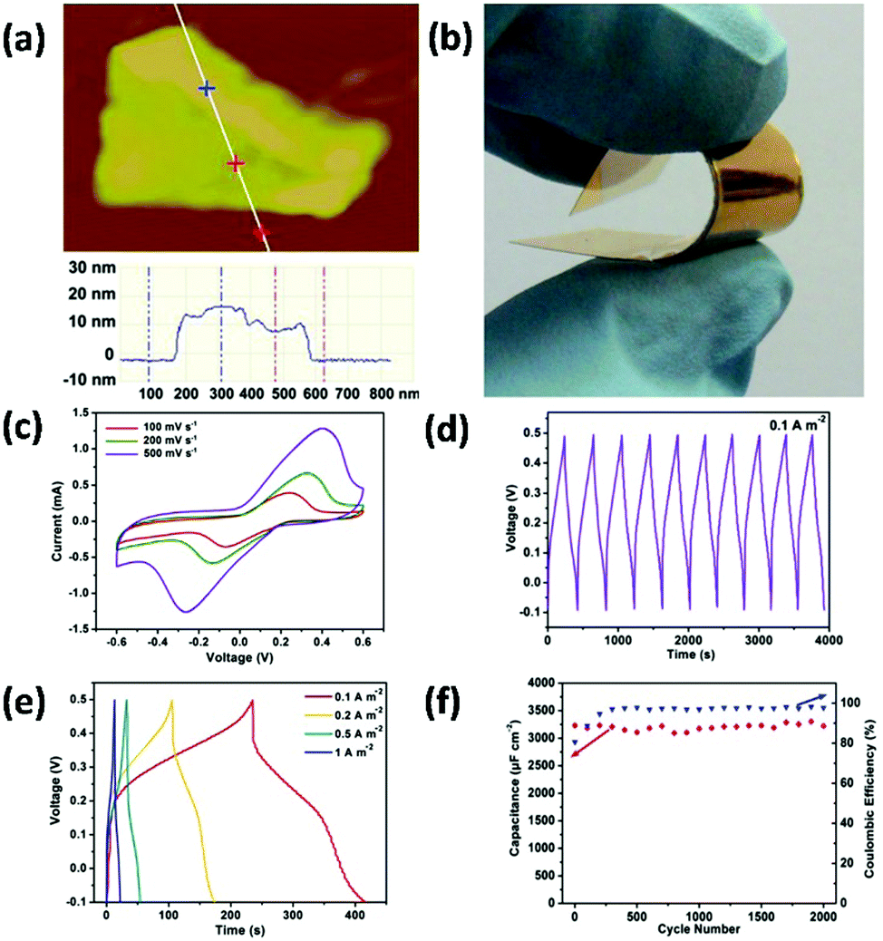 | ||
| Fig. 24 The β-Ni-LMH@G based thin-film electrode applied in an all-solid-state SC. (a) An AFM image of an individual flake of the exfoliated β-Ni-LMH@G. (b) A photo of the as-fabricated all-solid-state SC with an electrode area of 1 cm2, showing ultrathin configuration and excellent flexibility. (c) CV curves of the all-solid-state SC measured at different scan rates. (d) The first 10 cycles of galvanostatic charge/discharge curves at 0.1 A m−2. (e) Galvanostatic charge/discharge curves at different current densities. (f) A long-term stability investigation of the all-solid-state SC. Reproduced from ref. 229 with permission. Copyright 2018, Elsevier. | ||
Zhu et al. reported the electrophoretic deposition preparation of layered Ti3C2.101 Polypyrrole (PPy) was intercalated into the layered Ti3C2 by electrochemical polymerization. Free-standing Ti3C2 and PPy composite films (TC@PFs) were then obtained after being peeled off from substrates. Benefiting from their superior electrochemical performances and intrinsic flexibility, the free-standing TC@PFs were further used for fabricating an ultrathin, flexible, all-solid-state SC, which exhibited high capacitance, ultra-stable cycling performance, and excellent flex resistance.
Many other 2DLNs-based electrode active materials were also explored for their uses in flexible or/and stretchable SCs, and a supercapacitive performance comparison of some typical 2DLNs supported flexible SCs is summarized and listed in Table 3. Besides, as used in batteries, GO-based solid-state electrolytes were also widely employed to fabricate all-solid-state SCs,239,240 on which we will not go into details.
| Material | Specific capacitance and rate performance | Cyclic stability |
|---|---|---|
| Note: G@PSP: graphene and polyselenophene composite. GCLP: graphene and cellulose composite paper. 3DGHF: three-dimensional graphene hydrogel film. GCNNS: graphitic carbon nitride nanosheet. NHNP@FMSNS: Ni(OH)2 nanoplates incorporated flower-like MoS2 nanosheets. CONW@MONSA: Co3O4 nanowire (core) and MnO2 ultrathin nanosheet (shell) array. PNF: phosphorene nanoflake. h-BN@rGOF: hexagonal boron nitride and graphene hybrid film. GC + GOIGE: graphene doped carbon electrode, and graphene oxide doped ion gel electrolyte. rGO + AGO + rGO: H2SO4-intercalated graphene oxide electrolyte/separator, and reduced graphene oxide electrodes. | ||
| CBNPs@GP219 | 138 and 81.6 F g−1 at 10 and 500 mV s−1 (aqueous electrolyte), 83.2 F g−1 at 10 mV s−1 (organic electrolyte) | 3.85% and 4.35% capacitance loss after 2000 cycles at 10 A g−1 in aqueous and organic electrolytes, respectively |
| Crumpled GP221 | 196 and 125 F g−1 at 1 and 20 A g−1 under flat state | 4% capacitance loss after 1000 cycles at 10 A g−1 under a uniaxial strain of 200% |
| Fiber-like graphene assembly223 | 208.7 F g−1 (78.3 mF cm−2, 3.12 mF cm−1) at 0.1 A g−1, 155 F g−1 (58 mF cm−2, 2.33 mF cm−1) at 2 A g−1 | 1% capacitance loss after 5000 cycles at 1 A g−1 |
| β-Co-LMH226 | 2028 F g−1 at 5 A g−1, no available data for rate performance | 6.8% capacitance loss after 10000 cycles at 0.02 V s−1 (data from a full SC device) |
| FNS@CC227 | 52 and 36.5 mF cm−2 at 1 and 10 mA cm−2 | 19.5% capacitance loss after 2000 cycles at 2 mA cm−2 (data from a full SC device) |
| G@PSP230 | 305.4 and 280 F g−1 at 0.1 and 10 A g−1 | 5% capacitance loss after 5000 cycles at 0.4 A g−1 |
| GCLP231 | 120, 100, 75 and 40 F g−1 at 1, 10, 100 and 1000 mV s−1 | 0.9% capacitance loss after 5000 cycles at 0.05 V s−1 |
| N-Doped graphene232 | 282 and 165 F g−1 at 1 and 33 A g−1 | 0.2% and 30% capacitance loss after 10000 and 230000 cycles, respectively (current density not given) |
| 3DGHF233 | 186 and 130 F g−1 at 1 and 20 A g−1 | 8.4% capacitance loss after 10000 cycles at 10 A g−1 |
| β-Ni-LMH@GF229 | 3.30 and 2.12 mF cm−2 (660.8 and 424.0 F cm−3) at 100 and 1000 mA m−2 | Negligible capacitance loss after 2000 cycles (current density not given) |
| TC@PF101 | 203 and 132 mF cm−2 (406 and 264 F cm−3) at 1 and 10 mA cm−2 | Negligible capacitance loss after 20000 cycles (current density not given) |
| GCNNS234 | 259.4 and 140.8 F g−1 at 10 and 100 mV s−1 | No available data |
| NHNP@FMSNS235 | 516.4 and 244 F g−1 at 2 and 10 A g−1 | 5.8% capacitance loss after 9000 cycles at 1 V s−1 |
| CONW@MONSA236 | 480 and 267 F g−1 at 2.67 and 29.8 A g−1 | 2.7% capacitance loss after 5000 cycles at 11.25 mA cm−2 |
| PNF237 | 59.3, 48.5 and 14.2 F g−1 (17.78, 13.75 and 4.25 F cm−3) at 5, 10 and 90 mV s−1 | 15.5%, 19.7% and 28.2% capacitance loss after 10000, 20000 and 30000 cycles at 0.5 V s−1, respectively |
| h-BN@rGOF238 | 242, 220 and 160 F cm−3 at 10, 100 and 1000 mV s−1 | 1% capacitance loss after 10000 cycles at 0.3 V s−1 |
| GC + GOIGE239 | 190 and 160 F g−1 at 1 and 10 A g−1 | 20% capacitance loss after 5000 cycles at 10 A g−1 |
| rGO + AGO + rGO240 | 14.5 mF cm−2 at 0.5 mA, good rate performance evaluated by CV at scan rates varying from 0.05 to 0.6 V | 60% capacitance loss after 300 cycles at 0.5 mA (data from a full SC device) |
4.3. Two-dimensional layered nanomaterials supported flexible photovoltaics
PVs can convert light energy directly into electricity by photoelectric effects, which is an effective and ecofriendly way to harvest solar energy. Although Si solar cells (SSCs) still dominate the current PV market, other emerging PV technologies, such as dye sensitized solar cells (DSSCs), organic solar cells (OSCs), perovskite solar cells (PSCs), CuInGaSe solar cells (CIGSSCs), Schottky junction solar cells (SJSCs), and quantum dot sensitized solar cells (QDSSCs), have attracted increasing attention from both academia and industry.241 However, to fabricate high-performance PVs for wearable biomedical applications, numerous challenges still remain. For example, more high-performance intrinsically-flexible PV materials should be explored to further improve photoelectric conversion efficiency (PCE), deformability, and mechanical durability of PVs. Advanced PV structural designs and manufacturing techniques should also be applied to optimize the wearability of PVs.Owing to their superior mechanical, optical and electrical properties, 2DLNs are widely used in various types of flexible PVs as transparent electrodes, light absorption layers, and charge transport layers to improve overall performance of PVs.175 By an alkaline-etching method, Ruan and coworkers fabricated a flexible SSC, in which graphene was combined with ultrathin crystalline Si to construct a heterojunction (G@Si). Further studies confirmed that the graphene layer number could significantly affect the performance of the G@Si-based SSC.242 By performing surface passivation on Si, inserting a layer of poly(3-hexylthiophene) (P3HT) as an electron blocking layer, and controlling the graphene layer number, a high PCE of 8.42% could be achieved for a 40 μm-thick SSC with excellent flexibility and durability.
Liu et al. fabricated package-free OSCs on flexible PI substrates with CVD-grown highly doped multilayer graphene as top transparent electrodes, Ag films as bottom electrodes, and P3HT:phenyl C61-butyric acid methyl ester (P3HT:PCBM) as active layers.243 A double-layer graphene electrode-based OSC exhibited a maximum PCE of 3.2% and excellent flexibility. More importantly, electrodes with more graphene layers could effectively protect the OSC from air contamination due to the superior anti-permeability of multilayer graphene films to air, hence a package-free OSC design was successfully realized.
By synthesizing a poly(3,4-ethylenedioxythiophene) (PEDOT) and graphene composite (PEDOT@G) on a PET substrate, Lee et al. demonstrated the fabrication of a PEDOT@G-based counter electrode, which was further used in a flexible DSSC without using additional transparent conductive oxides.244 The use of graphene dramatically decreased surface resistance of the counter electrode, and a high PCE of 6.2% was achieved by the DSSC. The PEDOT@G film is a promising candidate material to eliminate the need for Pt and transparent conductive oxides in DSSC counter electrodes, thereby reducing production costs.
Using a graphene sheets-based barrier layer and a ZnO QDs-based electron transport layer, Ameen and coworkers fabricated a flexible PSC on ITO–PETs.245 The combination of graphene and ZnO effectively improved carrier transport and electron collection efficiency. Atmospheric plasma jet and O2 plasma treatments on ITO–PETs enhanced the surface-to-volume ratio, porosity, and structure of ZnO QDs, which substantially improved light-harvesting efficiency. The as-fabricated flexible PSC achieved a PCE of 9.73% with high photocurrent density and open circuit voltage.
Chen and coworkers fabricated a flexible photoelectrode by electrophoretic depositing CdSe QD-modified graphene (CdSeQD@G) on an ITO–PET.246 Graphene was used as a good conducting scaffold for electron capturing and transport. A PCE of ∼0.6% and an incident photon to current conversion efficiency of 17% were achieved by the CdSeQD@G-based QDSSC, owing to the highly efficient collection and transportation of photogenerated electrons from CdSe in the presence of graphene.
Ye et al. fabricated a SJSC based on a CdSe nanobelt and graphene nanosheet-based Schottky junction (CdSeNB@G).247Fig. 25a shows a schematic illustration of the CdSeNB@G-based SJSC. A In/Au ohmic electrode was prepared at one end of a CdSe nanobelt by a successive UV lithography, thermal evaporation, and lift-off process. A graphene film was made on the other end of the CdSe nanobelt with a developed graphene patterning method using UV lithography. Fig. 25b shows a SEM image of the as-fabricated SJSC. An Au electrode that can form an ohmic contact with the graphene film was used later on for welding purposes. Fig. 25c shows the room-temperature current–voltage characteristic of the SJSC under air mass 1.5 global illumination with an intensity of 100 mW cm−2. The SJSC exhibited excellent PV behaviors, such as an open circuit voltage of 0.51 V, a short circuit current density of 5.75 mA, and a PCE of 1.25%, which could be attributed to the finely constructed Schottky electrode fabricated by the developed graphene patterning method.
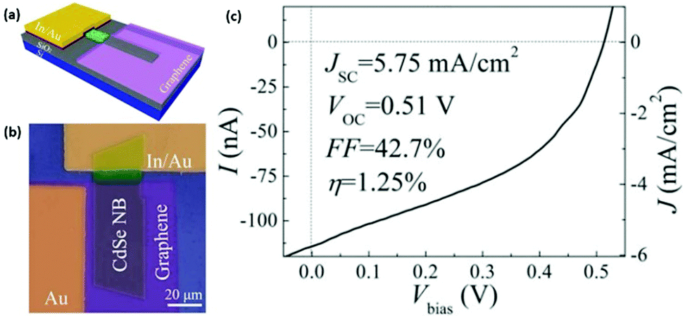 | ||
| Fig. 25 A CdSeNB@G-based SJSC. (a) Schematic of the CdSeNB@G-based SJSC. (b) A SEM image of the CdSeNB@G-based SJSC. (c) Room-temperature I–V characteristic of the SJSC under air mass 1.5 global illumination with an intensity of 100 mW cm−2. Reproduced from ref. 247 with permission. Copyright 2018, Royal Society of Chemistry. | ||
Through rationally designing device structures, highly efficient solar energy conversion and storage can be simultaneously realized. Based on the excellent photothermoelectric effect of graphene, Wang's group reported a graphene–CNT composite paper (GCP), which could convert solar/thermal energy into considerable current and voltage.248 By stacking this GCP with a heteroatom-doped GP-based P–N interface, a bifunctional device was fabricated incorporating a solar/thermal cell and a P–N junction capacitor. Simultaneous solar energy conversion and storage was achieved by this prototype device with a high charge-storage capacity of 70.5 μC cm−2 under one sun light intensity.
4.4. Two-dimensional layered nanomaterials supported flexible biofuel cells
The above-mentioned power supply systems, such as batteries, SCs and PVs, have been widely introduced to serve the energy demands of wearable electronics. However, batteries and SCs still suffer from frequent charging. The input energy of PVs (light) is also quite unstable under actual working conditions and difficult to offer a stable enough charging process, which cannot fully meet the demands of reliability in biomedical applications. Therefore, harvesting energy directly and mildly from a wearers' body to power WBEDs could be another attractive option, because of a minimized dependence on external energy sources.20 It is expected that wearable BFCs could help get close to this goal since they can utilize bacteria or enzymes catalyzed redox reactions to oxidize fuels from a human body (e.g., glucose, lactose) and produce electricity. By and large, BFCs can be classified into two major categories: microbial fuel cells (MFCs) and enzymatic biofuel cells (EBFCs).Mink et al. fabricated a flexible and sustainable micrometer-scale MFC, which employed CVD-grown graphene deposited on a Ni foam as anode, accompanied with an air cathode.250 Graphene can offer abundant attachment sites to bacteria and accelerate electron transfer on the anode, owing to its extremely high specific surface area and superior electron conductivity. Domestic waste water primary clarified by a local waste water treatment facility was added into the MFC to introduce the bacteria and allow a biofilm to grow on the anode. A waste water substitute containing a known concentration of an organic fuel was fed for performance analysis, and a ∼1 nW power was successfully achieved.
Wang et al. introduced a MFC with a flexible 3D graphene-loaded Ni foam as anode.251 The anode provided not only a large accessible surface area for microbial colonization and electron mediators, but also a uniform macroporous scaffold for effective mass diffusion of the culture medium. Significantly, at a steady state of power generation, the flexible MFC produced an optimal volumetric power density of 661 W m−3 calculated based on the volume of the anode material or 27 W m−3 calculated based on the volume of the anode chamber. Further studies showed that the MFC could be operated effectively in a batch-mode at least for a week.
Oxidants (generally, O2) are reduced on the cathode of a MFC. Slow oxygen reduction reaction (ORR) kinetics greatly limit the power density of MFCs, due to their high overpotentials. 2DLN-based MFC cathodes could either help lower ORR activation energy by improving ORR catalyst activity, or reduce current density by increasing specific surface area, both of which could effectively lower ORR overpotentials and help achieve higher MFC efficiency.249 Studies on this topic, especially for flexible MFCs, are still in their very infancy.
Although the above-mentioned flexible MFCs could exhibit some attractive performances, there are still some inherent limitations for them. Active sites of enzymes are buried deeply in microbe cells, which greatly hinders fuel access and drastically interferes with electron transfer. Therefore, higher power density can hardly be achieved. Furthermore, potential cytotoxicity is another inevitable problem when applying MFCs for WBEDs.20
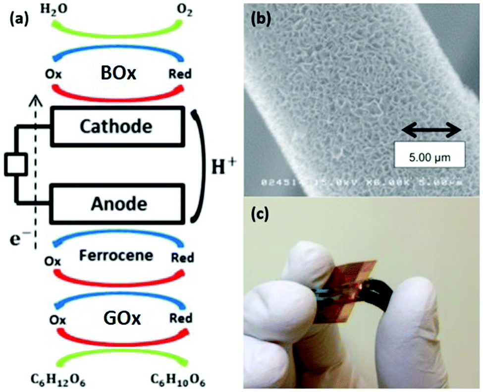 | ||
| Fig. 26 A flexible EBFC based on GCFC electrodes with glucose as biofuel. (a) A possible power generation mechanism of the glucose EBFC. (b) A SEM photo of the GCFC electrode. (c) A photo of the fabricated flexible EBFC. Reproduced from ref. 252 with permission. Copyright 2018, the Japan Society of Applied Physics. | ||
4.5. Two-dimensional layered nanomaterials supported flexible nanogenerators
NGs are a series of nanoscale generators that can convert thermal or mechanical energy produced by small-scale physical changes into electricity. Unlike batteries and SCs, they are self-powered systems without the demand of frequently charging from conventional external electric power supplies. Based on their energy sources, NGs can be mainly categorized into three different types, including thermoelectric, piezoelectric, and triboelectric NGs. Owing to their superior thermal, mechanical and electrical characteristics, 2DLNs are very powerful for constructing flexible NGs.20,255–257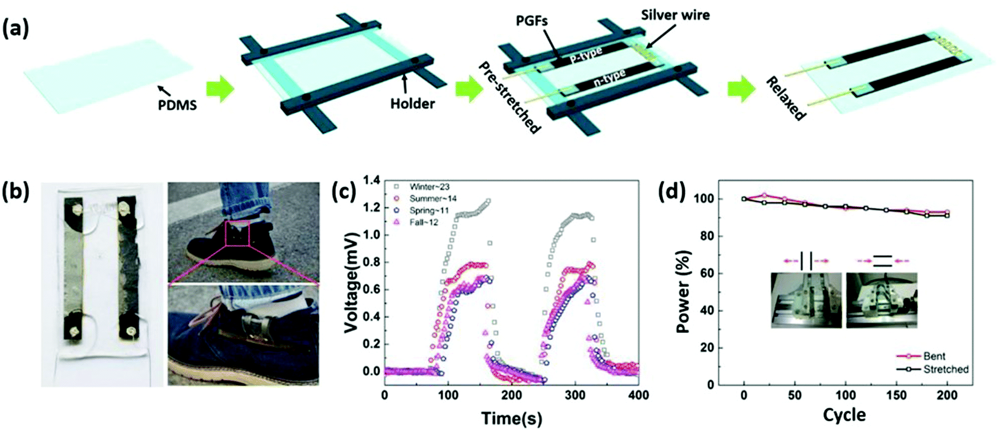 | ||
| Fig. 27 A flexible thermoelectric NG based on large-scale PAGFs. (a) Schematic of the fabrication process of the flexible thermoelectric NG on PDMS substrates. The device, consisting of a pair of legs, was pre-stretched by 25% with a holder before conglutinating. (b) A photo of the NG (left) and a typical application of using body heat to drive the NG by temperature difference between the inside and outside of a shoe (right). (c) Time-dependent voltage curves of the flexible thermoelectric NG at corresponding temperature differences. (d) Cycling stability tests of the flexible thermoelectric NG under 200 cycles of repeated stretching with an elongation of about 25% (left) or bending with a radius of about 8 mm (right). Reproduced from ref. 258 with permission. Copyright 2018, Elsevier. | ||
Triboelectric NGs are based on an integration of triboelectric effect and electrostatic induction.255 Based on the different forms of fractions, triboelectric NGs can be divided into three basic working modes: vertical contact-separation mode, lateral sliding mode, and single-electrode mode.255 A triboelectric potential can be cyclically induced between two triboelectric materials with oppositely polarized charges when periodic friction and separation are continuously performed, hence being capable of driving an alternating current flowing through an external circuit.261 When using 2DLNs as triboelectric materials, their high specific surface area and nanoscale surface roughness/friction could effectively promote interface charge separation.255 Shankaregowda et al. reported an arch shaped CVD-grown graphene-based triboelectric NG in the vertical contact-separation mode for collecting ambient vibration energy.262 By directly using graphene as one friction surface and PDMS as the other, a high output efficiency can be obtained during periodic contact and separation. A high open circuit voltage of 650 V and a short circuit current of 12 μA was achieved by an in-house made 3.5 cm × 4.5 cm triboelectric NG at the frequency of 4.3 Hz, and indicated that the triboelectric NG could be used as an efficient power device for wearable biomedical electronic applications.
5. Two-dimensional layered nanomaterials supported wearable integrated functional units for biomedical applications
With the increasing demands of WBEDs for multitask execution capabilities as well as lighter weight and smaller size, it is expected that advanced wearable integrated functional units will be developed that can realize the full utilization of material functionalities and structural spaces in WBEDs. Until now, many research efforts have been made on research orientations such as single wearable sensors for multiple signals, self-powered wearable sensors, and integrated wearable energy conversion and storage systems (IWECSSs),263–265 which obviously set a series of wonderful stages with diverse functionalities of 2DLNs given full play.It has been widely accepted that a more practical WBED should possess the ability to monitor several signals simultaneously in order to obtain a integrated dataset that can be utilized in a more comprehensive and intelligent health assessment.266 Researchers should make more effort towards integrating diverse signal sensing abilities into a single and small, but flexible and versatile platform. Based on two different graphene films, Xu et al. reported a multifunctional wearable sensor.267 The wearable sensor was designed with two sensing components: on the upper layer of the device, four kinds of porphyrin-modified rGO films were prepared and used for a sensor array that could sufficiently react with VOC vapors to achieve highly sensitive detection. A porous rGO film was designed on the underlayer of the device and used as a strain-sensing matrix that could be closely attached to the skin to achieve a highly sensitive detection of physiological signals. A PI film between the two sensing components was used not only as a flexible substrate, but also as a protective layer to avoid the porous rGO film's response to VOC vapors. The sensor could achieve simultaneous detection of physiological signals (e.g., pulse rate and respiration rate) and VOC biomarkers (e.g., acetone and NH3) without mutual signal interference. It should be noted that a multiple side-by-side sensing array might bring severe cross-talk among the individual sensors. Therefore, optimized circuit designs should be adopted to suppress interference and achieve more accurate signal recognition.
Wearable biomedical sensors with self-powering functions can effectively reduce their dependence on external power supply. Yang et al. reported a high-performance transparent and flexible triboelectric NG based on graphene and PEDOT:PSS composite electrodes via surface engineering.268 The schematic view is shown in Fig. 28a. The upper electrode consists of three parts including a PET film, a graphene layer, and a PEDOT:PSS layer, where the graphene–PEDOT:PSS bilayer film acts as the friction layer of the triboelectric NG. The lower electrode is a transparent PI film transferred onto a PET–graphene–PEDOT:PSS trilayer film, which acts as the dielectric friction layer of the triboelectric NG. PI tapes are used to construct a space between the two electrodes. Through modifying the CVD-grown graphene with PEDOT:PSS, composite electrodes were fabricated with high transmittance, low sheet resistance, and improved surface roughness. As a consequence, an output current density of 2.4 μA cm−2 and an output power of 12 μW was achieved by the triboelectric NG. The triboelectric NG could also be operated by the movement of human body joints to accumulate energy from body movements. The triboelectric NG was fixed on a finger joint, and its output voltages at different joint bending angles were measured (Fig. 28b). The results showed that the output voltage and the bending angle had a linear relationship with a correlation coefficient of 0.992 and a good linear sensitivity of 15.4 rad−1, thereby showing its potential as a self-powered wearable gesture sensor.
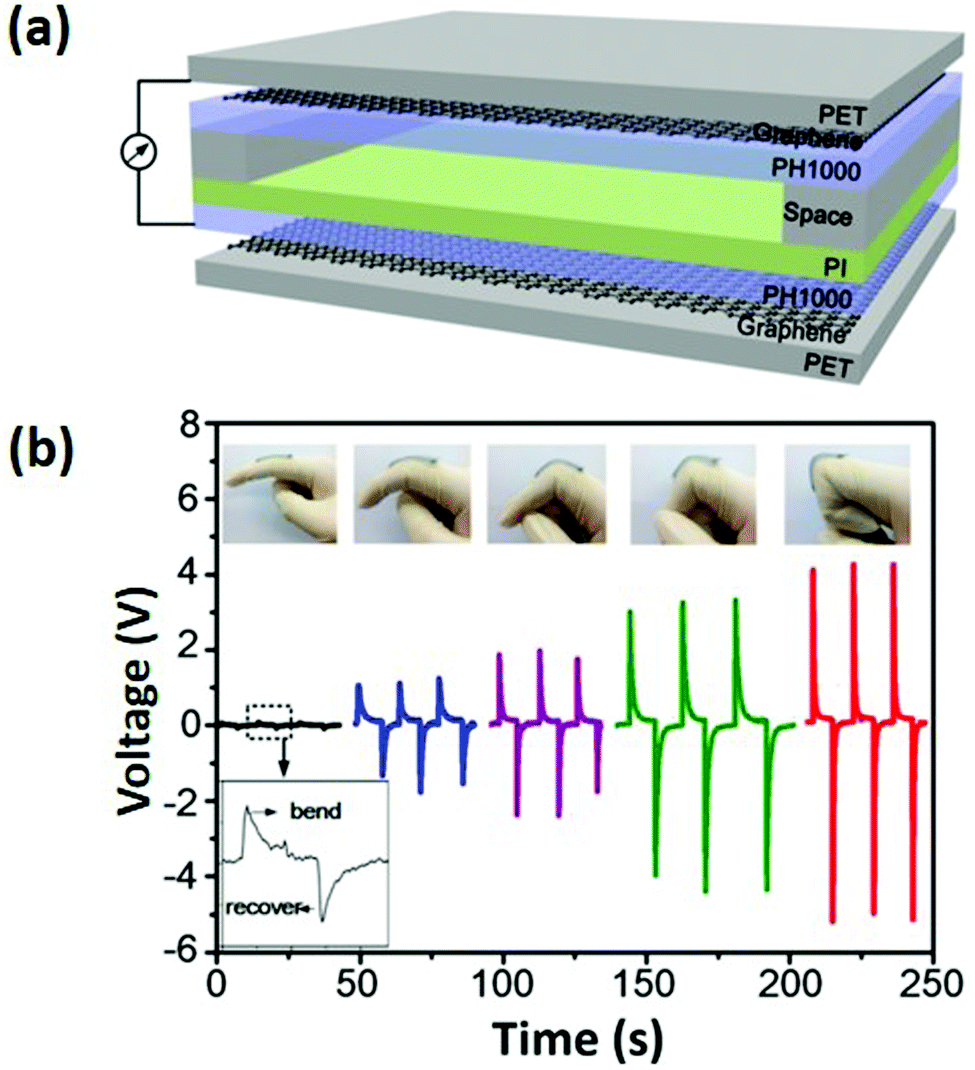 | ||
| Fig. 28 A transparent and flexible triboelectric NG based on surface engineered graphene and PEDOT:PSS composite electrodes. (a) Schematic of the triboelectric NG. PH1000 is a kind of commercial PEDOT:PSS product. (b) The output voltages of the NG at different finger joint bending angles. The inset shows the typical voltage signals at an angle of 30°. Reproduced from ref. 268 with permission. Copyright 2018, American Chemical Society. | ||
IWECSSs generally aim to collect small amounts of electric energies produced by energy conversion devices (e.g., PVs, BFCs, NGs), and store them into energy storage devices (e.g., batteries or SCs). The utilization of IWECSSs in WBEDs is very conducive to improving overall energy utilization efficiency and reducing maintenance requirements. For instance, Xue et al. introduced the first flexible self-charging power cell (SCPC).269 By using a kapton film as a supporting shell, a flexible graphene electrode and a piezoelectric PVDF separator were sealed in liquid electrolyte. The flexible SCPC contained a piezoelectric NG, a LIB, and a power-management system, and could directly be used as a wearable power device that converts mechanical energy into electrochemical energy (Fig. 29a). The flexible SCPC could be charged by either human body or machine movement, thus could be very useful for recycling and storing redundant mechanical energy in our living environment. Manjakkal et al. presented a flexible 3D porous graphene foam based SC (GFSC) with a layer-by-layer structure consisting of graphene sheets, Ag conductive epoxy, and a graphene foam.270 The GFSC showed excellent supercapacitive performances even under rigid mechanical conditions, which could be attributed to the benefit from highly conductive electrode constituents and a highly porous electrode structure (Fig. 29b). The GFSC was integrated with a flexible PV to fabricate a flexible self-charging power pack, which was successfully utilized to continuously power a wearable CuO nanorod based pH sensor (Fig. 29c). This fascinating advance could inspire more promising developments on fully self-powered WBEDs.
 | ||
| Fig. 29 (a) Schematic showing the design of a flexible SCPC. Graphene nanosheets composited Cu foil is used as anode; a layer of polarized PVDF film performs as separator; a LCO based mixture on Al foil is used as cathode; Kapton boards are used as shell. (b) Schematic of a flexible GFSC full cell consisting of two electrodes and its cross-sectional structure. (c) Schematic of a WBED consisting of a PV, a GFSC and a pH sensor for solar-self-powered pH sensing. Reproduced from ref. 269 and 270 with permission. Copyright 2018, John Wiley & Sons. Copyright 2018, Elsevier. | ||
6. Remaining challenges and possible solutions
2DLNs have exhibited their strong application potential in the area of WBEDs. Recently, many prominent efforts have been expended to explore novel 2DLNs-based materials and structures, and propose novel device designs for integrating them more effectively into WBEDs. However, several challenges for 2DLNs supported wearable sensors and power devices still remain and should be focused and tackled for the upcoming period.6.1. Remaining challenges for two-dimensional layered nanomaterials supported wearable sensors and possible solutions
As previously described, some 2DLNs-loaded conventional flexible plastic films, papers and textiles, as well as newly developed 2DLN-based flexible free-standing films, have been employed as important components to satisfy flexibility requirements of 2DLNs-supported wearable biomedical sensors. However, currently many of them can only offer little or no stretchability. Compared with flexibility, stretchability could be a more vital factor to determine if a WBED is capable of providing adequate conformality to body joints or some other special body parts, and have enough resilience to completely recover its original structure without affecting any functional features after complex motions. On the other hand, wider utilization of textiles as well as free-standing substrates such as GPs is restricted for sensing with tissues that are not usually covered with clothing, since a majority of consumers would prefer wearable biomedical sensors functioning in an inconspicuous way. To figure it out, combining 2DLNs with transparent polymer substrates with high flexibility and stretchability could be a good choice. PDMS or silicone elastomers have been preliminarily applied as wearable sensor substrates.271 However, reported studies were mainly focused on ameliorating conventional device configurations, and employing the self-assembly or coating of 1DNs or graphene.30,272,273 But, there are still few ‘beyond graphene’ 2DLNs that have been exploited in this direction. Another point of focus is that both 2DLNs and polymer substrates may lack enough breathability. These 2DLNs-loaded polymer substrates should only bring about minimal physiological impacts to target tissues, since any moisture or heat accumulation could bring interferences to sensing results.Anti-interference performance is a key index for wearable biomedical sensors since their performances could be directly affected by many varying parameters such as pH, ionic strength, temperature and humidity. Deviation from the optimal working condition can apparently give rise to performance fluctuation of sensors, thus impairing their sensing ability. This challenge mainly depends on the nature of core recognition elements. 2DLNs could serve as effective supports for loading enzymes and other bioreceptors.274 Optimizedly adopting 2DLNs could provide more biocompatible working environments for enzymes or bioreceptors and promote electron transfer, thereby achieving better comprehensive sensing performances.274 Besides, based on superior nonenzymatic biosensing capabilities of some composites of 2DLNs with metals or TMOs, more effort could be made to develop advanced nonenzymatic wearable biomedical sensors, reducing their activity dependence on enzymes or biomolecules.275
Moreover, microminiaturization and apparent concealability are also some quite valuable merits. User privacy is taken more into account nowadays, since scores of users prefer to use wearable biomedical sensors inconspicuously without receiving particular attention from others. More efficient integration of high-performance 2DLNs- or 2DLNs-based composites and achieving sensing functions with only one or few nanosheets could help downsize the full device from centimeter/millimeter to micrometer/nanometer scale. Therefore, this strategy is strongly expected in the future design and development of wearable biomedical sensors.276,277
Many conventional chemical/biological sensing methods require tedious sample pretreatment procedures in every detection process. These time-consuming procedures are adverse to realizing simple and rapid real-time sensing with wearable biomedical sensors. To address this, as we discussed before, integrating 2DLNs into core sensing components is quite useful since it could help achieve enhanced signal recognition with better sensitivity and selectivity. On the other hand, developing and utilizing highly selective rapid permeable membranes to conduct analyte separation prior to sensing processes could be another significant plan.278–280
Self-healing property is a very fascinating capability since it can help wearable sensors quickly in situ repair unexpected microscopic/mesoscopic mechanical or electronic damages on their own and recover their intact functions. Integration with self-healing property can indubitably further promote life-span and reliability of these devices. Some microcapsule-based healing strategies have been presented, in which microcapsules encapsulating healing agents were mixed into functional inks, and then directly printed onto flexible substrates.281 When the printed trace is damaged, the microcapsules along the crack will fracture to release the encapsulated healing agents (e.g., solvents for substrate dissolution and resolidification, conductive agents such as graphene, and CNTs) and restore the microstructure. This strategy could further improve the wearability of wearable sensors.
6.2. Remaining challenges for two-dimensional layered nanomaterials supported wearable power devices and possible solutions
Future commercial WBEDs are expected to detect multiple signals simultaneously and carry out complicated data processing and transmission, which has presented higher demands for relevant wearable power devices. Although a lot of impressive progress has been achieved, the application of 2DLNs in this hot area is still in its infancy. Comprehensive performances of these lab-developed prototype devices need to be improved substantially to target a more promising market foreground.Batteries, represented by LIBs, are still the most mature wearable power devices owing to their relatively long cycle life, high energy density, low self-discharge rate, and impressive shelf life.282 However, even though many attractive wearable battery systems have been presented, it is still very common that they are much heavier than the corresponding wearable appliances they are supposed to power. On the other hand, downsizing batteries, making them lighter and body-compliant, will inevitably lower their stored net energy and limit their lifetime.282 Many researchers are attempting to settle problems resulting from size and weight shrinking by taking advantage of 2DLNs- and 2DLNs-based nanocomposite assembled 3D microstructures to further improve energy density, cyclic, and rate performance.283 Their highly porous structure can help greatly enhance effective contact between electrolyte and active materials, improve efficiency of electrolyte diffusion and electron/ion transport, and provide good adjustment of strain induced by the volume change during electrochemical cycles. Heat management is another important aspect for highly reliable applications of LIBs. The overall performance of conventional LIBs will observably deteriorate when they work below subzero temperatures. Thermal runaway can probably occur as well under certain conditions, and overheating may result in self-ignition or even explosion. Furthermore, current LIB techniques still suffer from utilization of highly toxic electrode materials and caustic electrolytes. Considering the potential risk of explosion under failed heat management or other mechanical damages, the leakage of these hazardous materials may result in serious skin injury.284 To address the heat management problem, Chen et al. developed a thermoresponsive polymer-based protective coating for LIBs, which can turn off LIBs in the case of overheating.285 Wang et al. presented a LIB integrated with a self-heating function that can provide temperature compensation under low temperature.286 As typical 2DLNs, graphene possesses excellent thermal conductivity, whereas GO can exhibit superior heat insulation performance. The above results and diverse thermal properties of 2DLNs could inspire more explorations on developing WBEDs with wider operating temperature windows. Besides, for finally eliminating the risk from hazardous battery materials in wearable LIBs, adopting more water-phase electrolytes or solid ion conductors, or developing all-solid-state battery systems could be better choices.283
Although some examples of 2DLNs-supported SCs have exhibited quite good performance, as for batteries, tremendous efforts are still needed with the development and application of novel 2DLNs-supported SCs to achieve higher energy density, improved columbic efficiency, and longer cycling life. 2DLNs-based nanohybrids can achieve remarkable improvements in supercapacitive performances, owing to the high mechanical integrity and superior interplane electrical conductivity originating from 2DLN nanosheets (particularly, graphene), as well as enhanced electrochemical properties that come from pseudocapacitive materials, such as TMOs,287 TMCs,288 and MXenes.289 Heteroatom doping is also a very effective way to ameliorate the pseudocapacitive nature of 2DLNs.290 Besides, further improving 2DLNs-based flexible SCs by hybridizing 2DLNs with nanomaterials or nanostructures in other dimensions can restrain restacking of nanosheets and promote ion transport.291,292 Rational in situ modification of conductive polymers on 2DLNs is another significant method to improve the relatively poor interplane electrical conductivity of 2DLNs.293 Adopting a suitable organic or ionic liquid electrolyte can produce well-separated and highly stable potential windows, and the resulting high operation voltage can significantly increase energy density.294,295 In addition to material aspects, designing all-solid-state asymmetric SCs296 and utilizing advanced micro-/nano-machining technologies297 are quite admissible since they can provide enhanced safety and reliability.
Solar energy is currently considered as the most common source of harvestable clean energy. Nevertheless, major efforts are still required for adopting it as a possible energy source for reliable commercial wearable applications. The main problem of solar energy is its low density. Considering increasing energy demand from wearable sensors and other adjuncts, solar panels with very large surface areas are needed to harvest sufficient energy for continuous powering, which is intrinsically restricted by the actual installable area of normal clothes. Furthermore, changeable weather, uncertain body movement, and increasing indoor activities will notably affect PCE of PV panels, resulting in instability of a power supply. Besides, many types of conventional PVs are still facing the problem of applying expensive (e.g., monocrystalline Si) and toxic (e.g., As, In) materials. Further improving the PCE of PVs is currently a major theme by exploring PV materials and optimizing PV fabrication techniques. Reported studies mainly focused on the utilization of graphene, and there are still many members in the 2DLN family whose potentials have not been sufficiently exploited. Recently, many 2D perovskites-based flexible PVs have achieved quite high PCE as well as enhanced stability.298 Many 2D TMOs (e.g., ZnO, SnO2, TiO2) could also be employed as transparent semiconductor films in DSSCs.299–301 2D TMCs were also used as highly efficient hole-transporting materials of PSCs.302,303 In addition, some novel DSSCs have also been developed, which can generate power under both sun light and indoor light sources.304
One of the main challenges that hamper a wider use of EBFCs on WBEDs is the denaturation or inactivation of enzymes, especially under ever-changing operating environments encountered by WBEDs. Besides, it is also very difficult for wearable EBFCs to provide uprated power supply continuously and constantly, since it is still impossible to access a stable flow of biofuel with high concentration from a human body. Furthermore, the high instability of enzymes has also put forward higher requirements for packaging techniques with power devices. Adopting suitable enzyme stabilizing agents305 and mending microenvironments around bioelectrodes more biocompatible to immobilized enzymes306 could be very helpful for keeping high enzyme activity. To address the issue of stable and continuous power supply, some groups are developing multifuel BFCs307 and rechargeable BFCs,308 as well as new techniques to facilitate complete oxidation of fuels.309 Incorporating diverse 2DLNs-based nanohybrids into bioelectrodes to further promote biocatalytic reactions and improve power conversion efficiency is obviously also a feasible approach.310
Although NG looks to be a very seductive concept and some preliminary exploration in this area has achieved very attractive results, more effort should be made in order to address some subsistent issues. An in-depth understanding of charge transfer and energy conversion processes in NGs could provide important directive significance for further elevating energy conversion efficiency and improving output performances of NGs.311–313 Based on these results, further engineering the surface morphologies and properties of 2DLNs could facilitate their use in developing novel wearable NGs. From the perspective of practical applications, fabrication methods that are facile, cost-effective, and easy to scale-up should also be further explored. In addition, the development of innovative NG working modes is quite attractive.
7. Conclusions and outlook
People eagerly expect that rapid technological advancements with WBEDs could help them better monitor and maintain their health levels and improve their living quality expediently without arresting influences on their daily lives. With fast growth of requirements for advanced WBEDs, development of state-of-the-art wearable sensors and power devices with excellent overall performance is of great significance. During past decades, applications of nanomaterials in WBEDs have been extensively explored, and tremendous progress has been achieved. As a momentous new branch in the big family of nanomaterials, 2DLNs have exhibited great potential to further elevate the comprehensive performances of WBEDs, owing to their unique physicochemical properties. In this review, we summarized the development, status, and trend of WBEDs, typical synthetic methods of 2DLNs, and further introduced some representative advancements with 2DLNs-based flexible/stretchable sensors and power devices for wearable biomedical applications in recent years, and we highlighted the important roles of 2DLNs in these devices. Some typical 2DLNs-supported wearable integrated functional units have also been introduced. Remaining critical challenges and possible solutions in the future development of 2DLNs-based wearable sensors and power devices were also discussed. Compared with existing relevant products, novel 2DLNs-supported wearable sensors and power devices exhibited excellent and competitive performances and undoubtedly show great promise to revolutionize the area of WBEDs in the near future.Abbreviations
| 1D | One-dimensional |
| 1DN | One-dimensional nanomaterial |
| 2D | Two-dimensional |
| 2DLN | Two-dimensional layered nanomaterial |
| 2DNLN | Two-dimensional non-layered nanomaterial |
| 3D | Three-dimensional |
| AFM | Atomic force microscopy |
| Au@PBNP | Core–shell structured nanoparticle with Au nanoparticle core and Prussian blue shell |
| AuNP | Au nanoparticle |
| BFC | Biofuel cell |
| BOx | Bilirubin oxidase |
| BSTG | Bi2Se1.5Te1.5 and graphene nanocomposite |
| CBNP | Carbon black nanoparticle |
| CBNPs@GP | Carbon black nanoparticles pillared graphene paper |
| CCGA | Chemically converted graphene aerogel |
| CdSeNB@G | CdSe nanobelt and graphene nanosheet based Schottky junction |
| CdSeQD@G | CdSe quantum dot modified graphene |
| CIGSSC | CuInGaSe solar cell |
| CNT | Carbon nanotube |
| CV | Cyclic voltammetry |
| CVD | Chemical vapor deposition |
| DA | Dopamine |
| DSSC | Dye sensitized solar cell |
| E. coli | Escherichia coli |
| EBFC | Enzymatic biofuel cell |
| ECD | Electrochemical deposition |
| ECG | Electrocardiography |
| EDLC | Electrical double layer capacitance |
| EEG | Electroencephalogram |
| EMG | Electromyogram |
| EOG | Electrooculography |
| E-skin | Electronic skin |
| FET | Field-effect transistor |
| FNS@CC | γ-FeOOH nanosheets loaded carbon cloth |
| fSGO | Sulfonic acid functionalized GO |
| G@Si | Graphene and ultrathin crystalline Si heterojunction |
| GA@PF | Graphene–Ag nanocomposite doped poly(vinylidene fluoride) matrix |
| GCFC | Graphene-coated carbon fiber cloth |
| GCN | Graphitic carbon nitride |
| GCP | Graphene and carbon nanotube composite paper |
| GF | Gauge factor |
| GFSC | A flexible three-dimensional porous graphene foam based supercapacitor |
| GMSP | Graphene and MoS2 composite paper |
| GO | Graphene oxide |
| GOx | Glucose oxidase |
| GP | Graphene paper |
| G-putty | Graphene and Silly Putty composite |
| GRPP | Graphene and poly(3,4-ethylenedioxythiophene):poly(styrenesulfonate) composite |
| h-BN | Hexagonal boron nitride |
| HIV | Human immunodeficiency virus |
| IL | Ionic liquid |
| IoMT | Internet of medical things |
| ITO | Indium tin oxide |
| ITO–PET | Indium tin oxide modified polyethylene terephthalate film |
| IWECSS | Integrated wearable energy conversion and storage system |
| LCO | LiCoO2 |
| LE | Liquid exfoliation |
| LED | Light emitting diode |
| LFP | LiFePO4 |
| LFP@GF | LiFePO4 loaded graphene foam |
| LIB | Li-ion battery |
| LMH | Layered metal hydroxide |
| LMO | LiMn2O4 |
| LNMCO | LiNixMnyCo1−x−yO2 |
| LOD | Limit of detection |
| LSB | Li–S battery |
| LTO | Li4Ti5O12 |
| LTO@GF | Li4Ti5O12 loaded graphene foam cathode |
| ME | Mechanical exfoliation |
| MEA | Microelectrode array |
| MFC | Microbial fuel cell |
| MXene | Transition metal carbide |
| NCGOM | Functionalized nanocellulose and graphene oxide composite membrane |
| NG | Nanogenerator |
| NIL | Nanoimprint lithography |
| NVP@rGOP | Na3V2(PO4)3 nanoparticles loaded rGO paper |
| ORR | Oxygen reduction reaction |
| OSC | Organic solar cell |
| P3HT | Poly(3-hexylthiophene) |
| P3HT:PCBM | Poly(3-hexylthiophene):phenyl C-61-butyric acid methyl ester |
| PAGF | Porous all-graphene film |
| PANI | Polyaniline |
| PB | Prussian blue |
| PC | Pseudocapacitance |
| PCB | Printed circuit board |
| PCE | Photoelectric conversion efficiency |
| PDMS | Polydimethylsiloxane |
| PEDOT | Poly(3,4-ethylenedioxythiophene) |
| PEDOT:PSS | A mixture of poly(3,4-ethylenedioxythiophene) and poly(styrenesulfonate) |
| PEDOT@G | Poly(3,4-ethylenedioxythiophene) and graphene composite |
| PEO | Polyethylene oxide |
| PEOGOF | Polyethylene oxide and graphene oxide based film |
| PET | Polyethylene terephthalate |
| PI | Polyimide |
| PLD | Pulsed laser deposition |
| PNS | Phosphorene nanosheet |
| POC | Point-of-care |
| PPy | Polypyrrole |
| PSC | Perovskite solar cell |
| PSPA@G | Poly(styrenesulfonate)doped polyaniline and graphene nanocomposite |
| PSS | Poly(styrenesulfonate) |
| PtAuNP | Pt–Au alloy nanoparticle |
| PtAuNPs@rGO–CNT–IL@GP | Pt–Au alloy nanoparticles decorated, reduced graphene oxide, carbon nanotube and ionic liquid loaded free-standing graphene paper |
| PtNP | Pt nanoparticle |
| PU | Polyurethane |
| PV | Photovoltaic |
| PVA | Polyvinyl alcohol |
| PVD | Physical vapor deposition |
| PVDF | Poly(vinylidene fluoride) |
| QD | Quantum dot |
| QDSSC | Quantum dot sensitized solar cell |
| RF | Radio frequency |
| rGO | Reduced graphene oxide |
| rGO–PUS | Fractured reduced graphene oxide wrapped polyurethane sponge |
| RH | Relative humidity |
| SAW | Surface acoustic wave |
| Sb@rGOP | Sb nanoparticles loaded rGO paper |
| SC | Supercapacitor |
| SCPC | Self-charging power cell |
| SEM | Scanning electron microscope |
| SIB | Na-ion battery |
| SJSC | Schottky junction solar cell |
| SNR | Signal to noise ratio |
| SpO2 | Blood oxygen saturation |
| SSC | Si solar cell |
| TC@PF | Ti3C2 and polypyrrole composite film |
| TCC | Temperature coefficients of capacity |
| TCR | Temperature coefficients of resistance |
| THz | Terahertz |
| TMC | Transition metal chalcogenide |
| TMO | Transition metal oxide |
| UA | Uric acid |
| UOx | Uricase |
| UV | Ultraviolet |
| vdW | van der Waals |
| vdWE | van der Waals epitaxy |
| VOC | Volatile organic compound |
| WBED | Wearable biomedical electronic device |
| WCS | Wet chemical synthesis |
| ZOB | Zn–O2 battery |
| β-Co-LMH | Monolayer β-Co(OH)2 |
| β-Ni-LMH@G | β-Ni(OH)2 and graphene nanohybrid |
| β-Ni-LMH@GF | β-Ni(OH)2 and graphene nanohybrid film |
Conflicts of interest
There are no conflicts to declare.Acknowledgements
This work was supported by the Danish Council for Independent Research-Technology and Product Sciences (DFF-FTP to Q. C., Project No. 12-127447). X. C. is grateful for the support from the Chinese Scholarship Council (PhD scholarship No. 201406170040). C. H. thanks the financial support from Natural Science Foundation of China (No. 51603037) and Young Elite Scientists Sponsorship Program by CAST (2017QNRC001).References
- S. Choi, H. Lee, R. Ghaffari, T. Hyeon and D.-H. Kim, Adv. Mater., 2016, 28, 4203–4218 CrossRef CAS PubMed.
- E. Wilhelm, S. Siby, Y. Zhou, X. J. S. Ashok, M. Jayasuriya, S. Foong, J. Kee, K. L. Wood and N. O. Tippenhauer, IEEE Sens. J., 2016, 16, 8111–8123 Search PubMed.
- C. Paddock, http://www.medicalnewstoday.com/articles/312459.php, accessed August 2018.
- L. Edwards, http://www.pocket-lint.com/news/137530-smart-contact-lenses-what-s-the-story-so-far, accessed August 2018.
- H. Lee, T. K. Choi, Y. B. Lee, H. R. Cho, R. Ghaffari, L. Wang, H. J. Choi, T. D. Chung, N. Lu, T. Hyeon, S. H. Choi and D.-H. Kim, Nat. Nanotechnol., 2016, 11, 566–572 CrossRef CAS PubMed.
- A. C. Thompson, https://www.cnet.com/products/omron-healthcare-blood-pressure-monitor/preview/, accessed August 2018.
- A. Chang, https://www.tomsguide.com/us/pain-relief-devices-tested,news-24683.html, accessed August 2018.
- D. Son, J. Lee, S. Qiao, R. Ghaffari, J. Kim, J. E. Lee, C. Song, S. J. Kim, D. J. Lee, S. W. Jun, S. Yang, M. Park, J. Shin, K. Do, M. Lee, K. Kang, C. S. Hwang, N. Lu, T. Hyeon and D.-H. Kim, Nat. Nanotechnol., 2014, 9, 397–404 CrossRef CAS PubMed.
- Z. Bao and X. Chen, Adv. Mater., 2016, 28, 4177–4179 CrossRef CAS PubMed.
- Mordor Intelligence LLP, http://www.researchandmarkets.com/reports/3450607/global-wearable-medical-device-market-growth#rela6, accessed August 2018.
- Y. Liu, M. Pharr and G. A. Salvatore, ACS Nano, 2017, 11, 9614–9635 CrossRef CAS PubMed.
- S. Yao, P. Swetha and Y. Zhu, Adv. Healthcare Mater., 2018, 7, 1700889 CrossRef PubMed.
- L. Richardson, https://news.energysage.com/solar-energy-news-solar-disrupting-wearable-tech/, accessed August 2018.
- S.-S. Lee, K.-H. Choi, S.-H. Kim and S.-Y. Lee, Adv. Funct. Mater., 2018, 28, 1705571 CrossRef.
- A. J. Bandodkar, J.-M. You, N.-H. Kim, Y. Gu, R. Kumar, A. M. V. Mohan, J. Kurniawan, S. Imani, T. Nakagawa, B. Parish, M. Parthasarathy, P. P. Mercier, S. Xu and J. Wang, Energy Environ. Sci., 2017, 10, 1581–1589 RSC.
- Y.-H. Lee, J.-S. Kim, J. Noh, I. Lee, H. J. Kim, S. Choi, J. Seo, S. Jeon, T.-S. Kim, J.-Y. Lee and J. W. Choi, Nano Lett., 2013, 13, 5753–5761 CrossRef CAS PubMed.
- S. Xu, Y. Zhang, J. Cho, J. Lee, X. Huang, L. Jia, J. A. Fan, Y. Su, J. Su, H. Zhang, H. Cheng, B. Lu, C. Yu, C. Chuang, T. Kim, T. Song, K. Shigeta, S. Kang, C. Dagdeviren, I. Petrov, P. V. Braun, Y. Huang, U. Paik and J. A. Rogers, Nat. Commun., 2013, 4, 1543 CrossRef PubMed.
- G. Zhu, P. Bai, J. Chen and Z. L. Wang, Nano Energy, 2013, 2, 688–692 CrossRef CAS.
- S. Gong and W. Cheng, Adv. Energy Mater., 2017, 7, 1700648 CrossRef.
- A. J. Bandodkar and J. Wang, Electroanalysis, 2016, 28, 1188–1200 CrossRef CAS.
- E. Dib, M. Bescond, N. Cavassilas, F. Michelini, L. Raymond and M. Lannoo, J. Appl. Phys., 2013, 114, 083705 CrossRef.
- N. Lu and D. H. Kim, Soft Robot., 2013, 1, 53–62 CrossRef.
- L. Wen, F. Li and H.-M. Cheng, Adv. Mater., 2016, 28, 4306–4337 CrossRef CAS PubMed.
- J. A. Rogers, M. G. Lagally and R. G. Nuzzo, Nature, 2011, 477, 45–53 CrossRef CAS PubMed.
- K. R. Symon, Mechanics, Addison-Wesley, 3rd edn, 1971 Search PubMed.
- S. Logothetidis, Mater. Sci. Eng., B, 2008, 152, 96–104 CrossRef CAS.
- Y. Liu, K. He, G. Chen, W. R. Leow and X. Chen, Chem. Rev., 2017, 117, 12893–12941 CrossRef CAS PubMed.
- G. Chen, N. Matsuhisa, Z. Liu, D. Qi, P. Cai, Y. Jiang, C. Wan, Y. Cui, W. R. Leow, Z. Liu, S. Gong, K.-Q. Zhang, Y. Cheng and X. Chen, Adv. Mater., 2018, 30, 1800129 CrossRef PubMed.
- D. Pradhan, F. Niroui and K. T. Leung, ACS Appl. Mater. Interfaces, 2010, 2, 2409–2412 CrossRef CAS PubMed.
- S. M. Lee, H. J. Byeon, J. H. Lee, D. H. Baek, K. H. Lee, J. S. Hong and S. H. Lee, Sci. Rep., 2014, 4, 6074 CrossRef CAS PubMed.
- S. Gong and W. Cheng, Adv. Electron. Mater., 2017, 3, 1600314 CrossRef.
- C. Zhu, T. Liu, F. Qian, W. Chen, S. Chandrasekaran, B. Yao, Y. Song, E. B. Duoss, J. D. Kuntz, C. M. Spadaccini, M. A. Worsley and Y. Li, Nano Today, 2017, 15, 107–120 CrossRef CAS.
- Q. Yun, Q. Lu, X. Zhang, C. Tan and H. Zhang, Angew. Chem., Int. Ed., 2018, 57, 626–646 CrossRef CAS PubMed.
- Z. Lv, Y. Luo, Y. Tang, J. Wei, Z. Zhu, X. Zhou, W. Li, Y. Zeng, W. Zhang, Y. Zhang, D. Qi, S. Pan, X. J. Loh and X. Chen, Adv. Mater., 2018, 30, 1704531 CrossRef PubMed.
- K. S. Novoselov, A. K. Geim, S. V. Morozov, D. Jiang, Y. Zhang, S. V. Dubonos, I. V. Grigorieva and A. A. Firsov, Science, 2004, 306, 666–669 CrossRef CAS PubMed.
- J. Wan, S. D. Lacey, J. Dai, W. Bao, M. S. Fuhrer and L. Hu, Chem. Soc. Rev., 2015, 45, 6742–6765 RSC.
- C. Tan and H. Zhang, Nat. Commun., 2015, 6, 7873 CrossRef CAS PubMed.
- G. Yang, C. Zhu, D. Du, J. Zhu and Y. Lin, Nanoscale, 2015, 7, 14217 RSC.
- D. Chimene, D. L. Alge and A. K. Gaharwar, Adv. Mater., 2015, 27, 7261–7284 CrossRef CAS PubMed.
- M. Nurunnabi, K. Parvez, M. Nafiujjaman, V. Revuri, H. A. Khan and X. Feng, RSC Adv., 2015, 5, 42141–42161 RSC.
- V. Singh, D. Joung, L. Zhai, S. Das, S. I. Khondaker and S. Seal, Prog. Mater. Sci., 2011, 56, 1178–1271 CrossRef CAS.
- L. Ji, P. Meduri, V. Agubra, X. Xiao and M. Alcoutlabi, Adv. Energy Mater., 2016, 6, 1502159 CrossRef.
- A. Halder, M. Zhang and Q. Chi, Rev. Adv. Sci. Eng., 2016, 5, 4–31 CrossRef.
- A. Gupta, T. Sakthivel and S. Seal, Prog. Mater. Sci., 2015, 73, 44–126 CrossRef CAS.
- Z. Sun, T. Liao, Y. Dou, S. M. Hwang, M. S. Park, L. Jiang, J. H. Kim and S. X. Dou, Nat. Commun., 2014, 5, 3813 CrossRef CAS PubMed.
- B. Anasori, Y. Xie, M. Beidaghi, J. Lu, B. C. Hosler, L. Hultman, P. R. C. Kent, Y. Gogotsi and M. W. Barsoum, ACS Nano, 2015, 9, 9507–9516 CrossRef CAS PubMed.
- H. Liang, L. Li, F. Meng, L. Dang, J. Zhuo, A. Forticaux, Z. Wang and S. Jin, Chem. Mater., 2015, 27, 5702–5711 CrossRef CAS.
- M. Zelisko, Y. Hanlumyuang, S. Yang, Y. Liu, C. Lei, J. Li, P. M. Ajayan and P. Sharma, Nat. Commun., 2014, 5, 4284 CrossRef CAS PubMed.
- D. J. Perello, S. H. Chae, S. Song and Y. H. Lee, Nat. Commun., 2015, 6, 7809 CrossRef CAS PubMed.
- Q. H. Wang, K. Kalantar-Zadeh, A. Kis, J. N. Coleman and M. S. Strano, Nat. Nanotechnol., 2012, 7, 699–712 CrossRef CAS PubMed.
- T. T. Tran, K. Bray, M. J. Ford, M. Toth and I. Aharonovich, Nat. Nanotechnol., 2015, 11, 37–41 CrossRef PubMed.
- D. H. Cao, C. C. Stoumpos, O. K. Farha, J. T. Hupp and M. G. Kanatzidis, J. Am. Chem. Soc., 2015, 137, 7843–7850 CrossRef CAS PubMed.
- B. Huang, Y. Liu and Z. Xie, J. Mater. Chem. A, 2017, 5, 23481–23488 RSC.
- L. Gao, Small, 2017, 13, 1603994 CrossRef PubMed.
- K. Shavanova, Y. Bakakina, I. Burkova, I. Shtepliuk, R. Viter, A. Ubelis, V. Beni, N. Starodub, R. Yakimova and V. Khranovskyy, Sensors, 2016, 16, 223 CrossRef PubMed.
- C. Feng, Z. Lv, X. Yang and C. Wei, Phys. Chem. Chem. Phys., 2014, 16, 10464–10472 RSC.
- Z. Lv, Y. Chen, H. Wei, F. Li, Y. Hu, C. Wei and C. Feng, Electrochim. Acta, 2013, 111, 366–373 CrossRef CAS.
- C. Tan and H. Zhang, Chem. Soc. Rev., 2015, 44, 2713–2731 RSC.
- S. Jayabal, G. Saranya, J. Wu, Y. Liu, D. Geng and X. Meng, J. Mater. Chem. A, 2017, 5, 24540–24563 RSC.
- Y. Zhu, L. Peng, Z. Fang, C. Yan, X. Zhang and G. Yu, Adv. Mater., 2018, 30, 1706347 CrossRef PubMed.
- S. S. Varghese, S. H. Varghese, S. Swaminathan, K. K. Singh and V. Mittal, Electronics, 2015, 4, 651–687 CrossRef CAS.
- H. Zhang, ACS Nano, 2015, 9, 9451–9469 CrossRef CAS PubMed.
- Y. Dou, L. Zhang, X. Xu, Z. Sun, T. Liao and S. X. Dou, Chem. Soc. Rev., 2017, 46, 7338–7373 RSC.
- V. Nicolosi, M. Chhowalla, M. G. Kanatzidis, M. S. Strano and J. N. Coleman, Science, 2013, 340, 1226419 CrossRef.
- Y. Zhan, Z. Liu, S. Najmaei, P. M. Ajayan and J. Lou, Small, 2012, 8, 966–971 CrossRef CAS PubMed.
- M. I. Serna, S. H. Yoo, S. Moreno, Y. Xi, J. P. Oviedo, H. Choi, H. N. Alshareef, M. J. Kim, M. Minary-Jolandan and M. A. Quevedo-Lopez, ACS Nano, 2016, 10, 6054–6061 CrossRef CAS PubMed.
- X. Wan, K. Chen, Z. Chen, F. Xie, X. Zeng, W. Xie, J. Chen and J. Xu, Adv. Funct. Mater., 2017, 27, 1603998 CrossRef.
- X. Zhang, Z. Lai, C. Tan and H. Zhang, Angew. Chem., Int. Ed., 2016, 55, 2–25 CrossRef.
- C. Hou, M. Zhang, L. Zhang, Y. Tang, H. Wang and Q. Chi, Chem. Mater., 2017, 29, 1439–1446 CrossRef CAS.
- L. Jiao, L. Zhang, X. Wang, G. Diankov and H. Dai, Nature, 2009, 458, 877–880 CrossRef CAS PubMed.
- P. K. Kannan, D. J. Late, H. Morgan and C. S. Rout, Nanoscale, 2015, 7, 13293–13312 RSC.
- H. Li, J. Wu, Z. Yin and H. Zhang, Acc. Chem. Res., 2014, 47, 1067–1075 CrossRef CAS PubMed.
- H. Li, G. Lu, Y. Wang, Z. Yin, C. Cong, Q. He, L. Wang, F. Ding, T. Yu and H. Zhang, Small, 2013, 9, 1974–1981 CrossRef CAS PubMed.
- D. Pacilé, J. C. Meyer, Ç. Ö. Girit and A. Zettl, Appl. Phys. Lett., 2008, 92, 133107 CrossRef.
- W. S. Hummers Jr and R. E. Offeman, J. Am. Chem. Soc., 1958, 80, 1339 CrossRef.
- J. Xu, D. K. Dang, V. T. Tran, X. Liu, J. S. Chung, S. H. Hur, W. M. Choi, E. J. Kim and P. A. Kohl, J. Colloid Interface Sci., 2014, 418, 37–42 CrossRef CAS PubMed.
- M. Rong, L. Lin, X. Song, Y. Wang, Y. Zhong, J. Yan, Y. Feng, X. Zeng and X. Chen, Biosens. Bioelectron., 2015, 68, 210–217 CrossRef CAS PubMed.
- J. N. Coleman, M. Lotya, A. O’Neill, S. D. Bergin, P. J. King, U. Khan, K. Young, A. Gaucher, S. De, R. J. Smith, I. V. Shvets, S. K. Arora, G. Stanton, H. Y. Kim, K. Lee, G. T. Kim, G. S. Duesberg, T. Hallam, J. J. Boland, J. J. Wang, J. F. Donegan, J. C. Grunlan, G. Moriarty, A. Shmeliov, R. J. Nicholls, J. M. Perkins, E. M. Grieveson, K. Theuwissen, D. W. McComb, P. D. Nellist and V. Nicolosi, Science, 2011, 331, 568–571 CrossRef CAS PubMed.
- D. Hanlon, C. Backes, T. M. Higgins, M. Hughes, A. O’Neill, P. King, N. McEvoy, G. S. Duesberg, B. M. Sanchez, H. Pettersson, V. Nicolosi and J. N. Coleman, Chem. Mater., 2014, 26, 1751–1763 CrossRef CAS.
- Y. Lin, T. V. Williams and J. W. Connell, J. Phys. Chem. Lett., 2010, 1, 277–283 CrossRef CAS.
- G.-H. Yang, J.-J. Shi, S. Wang, W.-W. Xiong, L.-P. Jiang, C. Burda and J.-J. Zhu, Chem. Commun., 2013, 49, 10757–10759 RSC.
- I. Banerjee, T. Faris, Z. Stoeva, P. G. Harris, J. Chen, A. K. Sharma and A. K. Ray, 2D Mater., 2017, 4, 015036 CrossRef.
- Z. Zeng, T. Sun, J. Zhu, X. Huang, Z. Yin, G. Lu, Z. Fan, Q. Yan, H. H. Hng and H. Zhang, Angew. Chem., Int. Ed., 2012, 51, 9052–9056 CrossRef CAS PubMed.
- Y. Ebina, T. Sasaki and M. Watanabe, Solid State Ionics, 2002, 151, 177–182 CrossRef CAS.
- K. Lee, R. Gatensby, N. McEvoy, T. Hallam and G. S. Duesberg, Adv. Mater., 2013, 25, 6699–6702 CrossRef CAS PubMed.
- J. Yu, J. Li, W. Zhang and H. Chang, Chem. Sci., 2015, 6, 6705–6716 RSC.
- W. Auwärter, H. U. Suter, H. Sachdev and T. Greber, Chem. Mater., 2004, 16, 343–345 CrossRef.
- S. R. Jian, S. A. Ku, C. W. Luo and J. Y. Juang, Nanoscale Res. Lett., 2012, 7, 403 CrossRef PubMed.
- Z. Yang, J. Hao, S. Yuan, S. Lin, H. M. Yau, J. Dai and S. P. Lau, Adv. Mater., 2015, 27, 3748–3754 CrossRef CAS PubMed.
- O. S. Panwar, A. K. Kesarwani, S. R. Dhakate, B. P. Singh, R. K. Rakshit, A. Bisht and S. Chockalingam, J. Vac. Sci. Technol., B, 2013, 31, 040602 CrossRef.
- Y. Liu, L. Ren, Z. Zhang, X. Qi, H. Li and J. Zhong, Sci. Rep., 2016, 6, 22516 CrossRef CAS PubMed.
- J. Du, G. Zhou, H. Zhang, C. Cheng, J. Ma, W. Wei, L. Chen and T. Wang, ACS Appl. Mater. Interfaces, 2013, 5, 7405–7409 CrossRef CAS PubMed.
- Q. Yang, Z. Lu, J. Liu, X. Lei, Z. Chang, L. Luo and X. Sun, Prog. Nat. Sci.: Mater. Int., 2013, 23, 351–366 CrossRef.
- C. Hou, M. Zhang, T. Kasama, C. Engelbrekt, L. Zhang, H. Wang and Q. Chi, Adv. Mater., 2016, 28, 4097–4104 CrossRef CAS PubMed.
- P. Nautiyal, A. Loganathan, R. Agrawal, B. Boesl, C. Wang and A. Agarwal, Sci. Rep., 2016, 6, 29498 CrossRef PubMed.
- C. Nethravathi, A. A. Jeffery, M. Rajamathi, N. Kawamoto, R. Tenne, D. Golberg and Y. Bando, ACS Nano, 2013, 7, 7311–7317 CrossRef CAS PubMed.
- S. J. Rowley-Neale, E. P. Randviir, A. S. Abo Dena and C. E. Banks, Appl. Mater. Today, 2018, 10, 218–226 CrossRef.
- Y. L. Zhong, Z. Tian, G. P. Simon and D. Li, Mater. Today, 2015, 18, 73–78 CrossRef CAS.
- K. Parvez, S. Yang, X. Feng and K. Müllen, Synth. Met., 2015, 210, 123–132 CrossRef CAS.
- A. Cabrero-Vilatela, R. S. Weatherup, P. Braeuninger-Weimer, S. Caneva and S. Hofmann, Nanoscale, 2016, 8, 2149–2158 RSC.
- M. Zhu, Y. Huang, Q. Deng, J. Zhou, Z. Pei, Q. Xue, Y. Huang, Z. Wang, H. Li, Q. Huang and C. Zhi, Adv. Energy Mater., 2016, 6, 1600969 CrossRef.
- W. Zhai, C. Wang, P. Yu, Y. Wang and L. Mao, Anal. Chem., 2014, 86, 12206–12213 CrossRef CAS PubMed.
- Z. Lu, Z. Chang, W. Zhu and X. Sun, Chem. Commun., 2011, 47, 9651–9653 RSC.
- J. Song, L. Xu, J. Li, J. Xue, Y. Dong, X. Li and H. Zeng, Adv. Mater., 2016, 28, 4861–4869 CrossRef CAS PubMed.
- J. Shen, Y. Zhu, H. Jiang and C. Li, Nano Today, 2016, 11, 483–520 CrossRef CAS.
- W. Gong, C. Hou, Y. Guo, J. Zhou, J. Mu, Y. Li, Q. Zhang and H. Wang, Nano Energy, 2017, 39, 673–683 CrossRef CAS.
- Y. Liu, Q. Shi, C. Hou, Q. Zhang, Q. Li and H. Wang, Carbon, 2017, 125, 352–359 CrossRef CAS.
- Y. Khan, A. E. Ostfeld, C. M. Lochner, A. Pierre and A. C. Arias, Adv. Mater., 2016, 28, 4373–4395 CrossRef CAS PubMed.
- T. V. Tam, S. H. Hur, J. S. Chung and W. M. Choi, Sens. Actuators, A, 2015, 233, 368–373 CrossRef CAS.
- M. Shojaee, Sh. Nasresfahani, M. K. Dordane and M. H. Sheikhi, Sens. Actuators, A, 2018, 279, 448–456 CrossRef CAS.
- T. Wang, Y. Guo, P. Wan, H. Zhang, X. Chen and X. Sun, Small, 2016, 12, 3748–3756 CrossRef CAS PubMed.
- P. R. N. Childs, J. R. Greenwood and C. A. Long, Rev. Sci. Instrum., 2000, 71, 2959 CrossRef CAS.
- Y. Guo, C. Dun, J. Xu, J. Mu, P. Li, L. Gu, C. Hou, C. A. Hewitt, Q. Zhang, Y. Li, D. L. Carroll and H. Wang, Small, 2017, 13, 1702645 CrossRef PubMed.
- H. Zhan, G. Zhang, C. Yang and Y. Gu, J. Phys. Chem. C, 2018, 122, 7605–7612 CrossRef CAS.
- V.-T. Tran, J. Saint-Martin, P. Dollfus and S. Volz, Sci. Rep., 2017, 7, 2313 CrossRef PubMed.
- H. Song, J. Liu, B. Liu, J. Wu, H.-M. Cheng and F. Keng, Joule, 2018, 2, 442–463 CrossRef CAS.
- K. K. Sadasivuni, A. Kafy, H. C. Kim, H. U. Ko, S. Mun and J. Kim, Synth. Met., 2015, 206, 154–161 CrossRef CAS.
- T. Vuorinen, J. Niittynen, T. Kankkunen, T. M. Kraft and M. Mäntysalo, Sci. Rep., 2016, 6, 35289 CrossRef CAS PubMed.
- C. Hou, H. Wang, Q. Zhang, Y. Li and M. Zhu, Adv. Mater., 2014, 26, 5018–5024 CrossRef CAS PubMed.
- M. Jian, C. Wang, Q. Wang, H. Wang, K. Xia, Z. Yin, M. Zhang, X. Liang and Y. Zhang, Sci. China Mater., 2017, 60, 1026–1062 CrossRef.
- G. Ge, W. Huang, J. Shao and X. Dong, J. Semicond., 2018, 39, 011012 CrossRef.
- Y. Ma, N. Liu, L. Li, X. Hu, Z. Zou, J. Wang, S. Luo and Y. Gao, Nat. Commun., 2017, 8, 1207 CrossRef PubMed.
- H.-B. Yao, J. Ge, C.-F. Wang, X. Wang, W. Hu, Z.-J. Zheng, Y. Ni and S.-H. Yu, Adv. Mater., 2013, 25, 6692–6698 CrossRef CAS PubMed.
- M.-Y. Tsai, A. Tarasov, Z. R. Hesabi, H. Taghinejad, P. M. Campbell, C. A. Joiner, A. Adibi and E. M. Vogel, ACS Appl. Mater. Interfaces, 2015, 7, 12850–12855 CrossRef CAS PubMed.
- C. S. Boland, U. Khan, G. Ryan, S. Barwich, R. Charifou, A. Harvey, C. Backes, Z. Li, M. S. Ferreira, M. E. Möbius, R. J. Young and J. N. Coleman, Science, 2016, 354, 1257–1260 CrossRef CAS PubMed.
- W. Wu, L. Wang, Y. Li, F. Zhang, L. Lin, S. Niu, D. Chenet, X. Zhang, Y. Hao, T. F. Heinz, J. Hone and Z. L. Wang, Nature, 2014, 514, 470–474 CrossRef CAS PubMed.
- K.-A. N. Duerloo, M. T. Ong and E. J. Reed, J. Phys. Chem. Lett., 2012, 3, 2871–2876 CrossRef CAS.
- W. Feng, W. Zheng, F. Gao, X. S. Chen, G. Liu and T. Hasan, Chem. Mater., 2016, 28, 4278–4283 CrossRef CAS.
- A. Alzahrani, S. Hu, V. Azorin-Peris, L. Barrett, D. Esliger and M. Hayes, Sensors, 2015, 15, 25681–25702 CrossRef PubMed.
- C. Xie, C. Mak, X. Tao and G. Yan, Adv. Funct. Mater., 2017, 27, 1603886 CrossRef.
- Z. Sun and H. Chang, ACS Nano, 2014, 8, 4133–4156 CrossRef CAS PubMed.
- F. H. L. Koppens, T. Mueller, P. Avouris, A. C. Ferrari, M. S. Vitiello and M. Polini, Nat. Nanotechnol., 2014, 9, 780–793 CrossRef CAS PubMed.
- Z. Zheng, T. Zhang, J. Yao, Y. Zhang, J. Xu and G. Yang, Nanotechnology, 2016, 27, 225501 CrossRef PubMed.
- J. Song, J. Yuan, F. Xia, J. Liu, Y. Zhang, Y. L. Zhong, J. Zheng, Y. Liu, S. Li, M. Zhao, Z. Tian, R. A. Caruso, K. P. Loh and Q. Bao, Adv. Electron. Mater., 2016, 2, 1600077 CrossRef.
- M. Rivas, E. Rojas, M. C. Araya and G. M. Calaf, Oncol. Lett., 2015, 10, 2259–2264 CrossRef CAS PubMed.
- Q. Wang, K. Xu, Z. Wang, F. Wang, Y. Huang, M. Safdar, X. Zhan, F. Wang, Z. Cheng and J. He, Nano Lett., 2015, 15, 1183–1189 CrossRef CAS PubMed.
- R. B. Reilly and T. C. Lee, Technol. Health Care, 2010, 18, 443–458 Search PubMed.
- S. K. Ameri, R. Ho, H. Jang, L. Tao, Y. Wang, L. Wang, D. M. Schnyer, D. Akinwande and N. Lu, ACS Nano, 2017, 11, 7634–7641 CrossRef PubMed.
- C. Lou, R. Li, Z. Li, T. Liang, Z. Wei, M. Run, X. Yan and X. Liu, Sensors, 2016, 16, 1833 CrossRef PubMed.
- M. A. Calderón, A. Linneberg, J. Kleine-Tebbe, F. De Blay, D. H. F. De Rojas, J. C. Virchow and P. Demoly, J. Allergy Clin. Immunol., 2015, 136, 38–48 CrossRef PubMed.
- P. Salvo, F. D. Francesco, D. Costanzo, C. Ferrari, M. G. Trivella and D. De Rossi, IEEE Sens. J., 2010, 10, 1557–1558 Search PubMed.
- V. K. Tomer, N. Thangaraj, S. Gahlot and K. Kailasam, Nanoscale, 2016, 8, 19794–19803 RSC.
- P. He, J. R. Brent, H. Ding, J. Yang, D. J. Lewis, P. O’Brien and B. Derby, Nanoscale, 2018, 10, 5599–5606 RSC.
- P. Yasaei, A. Behranginia, T. Foroozan, M. Asadi, K. Kim, F. Khalili-Araghi and A. Salehi-Khojin, ACS Nano, 2015, 9, 9898–9905 CrossRef CAS PubMed.
- S. Borini, R. White, D. Wei, M. Astley, S. Haque, E. Spigone, N. Harris, J. Kivioja and T. Ryhänen, ACS Nano, 2013, 7, 11166–11173 CrossRef CAS PubMed.
- W. P. Xuan, J. K. Chen, X. L. He, W. B. Wang, S. R. Dong and J. K. Luo, Procedia Eng., 2015, 120, 364–367 CrossRef CAS.
- E. Singh, M. Meyyappan and H. S. Nalwa, ACS Appl. Mater. Interfaces, 2017, 9, 34544–34586 CrossRef CAS PubMed.
- W. He, Y. Sun, J. Xi, A. A. M. Abdurhman, J. Ren and H. Duan, Anal. Chim. Acta, 2016, 903, 61–68 CrossRef CAS PubMed.
- S. Liu, K. S. Hui and K. N. Hui, ACS Appl. Mater. Interfaces, 2016, 8, 3258–3267 CrossRef CAS PubMed.
- P. Labroo and Y. Cui, Biosens. Bioelectron., 2013, 41, 852–856 CrossRef CAS PubMed.
- A. M. H. Ng, Kenry, C. T. Lim, H. Y. Low and K. P. Loh, Biosens. Bioelectron., 2015, 65, 265–273 CrossRef CAS PubMed.
- X. Zan, H. Bai, C. Wang, F. Zhao and H. Duan, Chem. – Eur. J., 2016, 22, 5204–5210 CrossRef CAS PubMed.
- M. Zhang, A. Halder, C. Hou, J. Ulstrup and Q. Chi, Bioelectrochemistry, 2016, 109, 87–94 CrossRef CAS PubMed.
- N. Zhu, S. Han, S. Gan, J. Ulstrup and Q. Chi, Adv. Funct. Mater., 2013, 23, 5297–5306 CrossRef CAS.
- B. Mailly-Giacchetti, A. Hsu, H. Wang, V. Vinciguerra, F. Pappalardo, L. Occhipinti, E. Guidetti, S. Coffa, J. Kong and T. Palacios, J. Appl. Phys., 2013, 114, 084505 CrossRef.
- D. Kinnamon, R. Ghanta, K.-C. Lin, S. Muthukumar and S. Prasad, Sci. Rep., 2017, 7, 13312 CrossRef PubMed.
- C. Liao, C. Mak, M. Zhang, H. L. W. Chan and F. Yan, Adv. Mater., 2015, 27, 676–681 CrossRef CAS PubMed.
- G. Jiang, M. Goledzinowski, F. J. E. Comeau, H. Zarrin, G. Lui, J. Lenos, A. Veileux, G. Liu, J. Zhang, S. Hemmati, J. Qiao and Z. Chen, Adv. Funct. Mater., 2016, 26, 1729–1736 CrossRef CAS.
- Y. J. Yun, W. G. Hong, N. J. Choi, B. H. Kim, Y. Jun and H. K. Lee, Sci. Rep., 2015, 5, 10904 CrossRef CAS PubMed.
- S. Sayed, A. A. El-Moneim, A. M. R. F. El-Bab and K. Nakamura, Int. J. Adv. Res. Technol., 2015, 4, 518–523 Search PubMed.
- Y. Seekaew, S. Lokavee, D. Phokharatkul, A. Wisitsoraat, T. Kerdcharoen and C. Wongchoosuk, Org. Electron., 2014, 15, 2971–2981 CrossRef CAS.
- S. Cho, J. S. Lee, J. Jun, S. G. Kim and J. Jang, Nanoscale, 2014, 6, 15181–15195 RSC.
- Y. Yamada, K. Ohtani, A. Imajo, H. Izu, H. Nakamura and K. Shiraishi, Toxicol. Rep., 2015, 2, 729–736 CrossRef CAS PubMed.
- J. Choi, S. Pyo, K. Lee, H. J. Ko and J. Kim, The 26th IEEE International Conference on Micro Electro Mechanical Systems, Taipei, Taiwan, IEEE, 2013, pp. 512–515.
- P. K. Basu, D. Indukuri, S. Keshavan, V. Navratna, S. R. K. Vanjari, S. Raghavan and N. Bhat, Sens. Actuators, B, 2014, 190, 342–347 CrossRef CAS.
- M. S. Mannoor, H. Tao, J. D. Clayton, A. Sengupta, D. L. Kaplan, R. R. Naik, N. Verma, F. G. Omenetto and M. C. McAlpine, Nat. Commun., 2012, 3, 763 CrossRef PubMed.
- D. Son, S. I. Chae, M. Kim, M. K. Choi, J. Yang, K. Park, V. S. Kale, J. H. Koo, C. Choi, M. Lee, J. H. Kim, T. Hyeon and D. H. Kim, Adv. Mater., 2016, 28, 9326–9332 CrossRef CAS PubMed.
- F. Zhao, H. Cheng, Y. Hu, L. Song, Z. Zhang, L. Jiang and L. Qu, Sci. Rep., 2014, 4, 5882 CrossRef CAS PubMed.
- W. Zhu, M. N. Yogeesh, S. Yang, S. H. Aldave, J. S. Kim, S. Sonde, L. Tao, N. Lu and D. Akinwande, Nano Lett., 2015, 15, 1883–1890 CrossRef CAS PubMed.
- X. Huang, T. Leng, M. Zhu, X. Zhang, J. C. Chen, K. H. Chang, M. Aqeeli, A. K. Geim, K. S. Novoselov and Z. Hu, Sci. Rep., 2015, 5, 18298 CrossRef CAS PubMed.
- T. Wang, H. Yang, D. Qi, Z. Liu, P. Cai, H. Zhang and X. Chen, Small, 2018, 14, 1702933 CrossRef PubMed.
- O. S. Kwon, S. H. Lee, S. J. Park, J. H. An, H. S. Song, T. Kim, J. H. Oh, J. Bae, H. Yoon, T. H. Park and J. Jang, Adv. Mater., 2013, 25, 4177–4185 CrossRef CAS PubMed.
- F. Withers, O. Del Pozo-Zamudio, A. Mishchenko, A. P. Rooney, A. Gholinia, K. Watanabe, T. Taniguchi, S. J. Haigh, A. K. Geim, A. I. Tartakovskii and K. S. Novoselov, Nat. Mater., 2015, 14, 301–306 CrossRef CAS PubMed.
- R. J. Mortimer, Annu. Rev. Mater. Res., 2011, 41, 241–268 CrossRef CAS.
- H. Li, J. Wang, Q. Shi, M. Zhang, C. Hou, G. Shi, H. Wang, Q. Zhang, Y. Li and Q. Chi, Appl. Surf. Sci., 2016, 380, 281–287 CrossRef CAS.
- P. Cai, B. Hu, W. R. Leow, X. Wang, X. J. Loh, Y.-L. Wu and X. Chen, Adv. Mater., 2018, 30, 1800572 CrossRef PubMed.
- A. Nisar, N. Afzulpurkar, B. Mahaisavariya and A. Tuantranont, Sens. Actuators, B, 2008, 130, 917–942 CrossRef CAS.
- J. He, P. Xiao, J. Zhang, Z. Liu, W. Wang, L. Qu, Q. Ouyang, X. Wang, Y. Chen and T. Chen, Adv. Mater. Interfaces, 2016, 3, 1600169 CrossRef.
- S. J. Varma, K. S. Kumar, S. Seal, S. Rajaraman and J. Thomas, Adv. Sci., 2018, 5, 1800340 CrossRef PubMed.
- J. Liu, H. Cao, B. Jiang, Y. Xue and L. Fu, Sci. China Mater., 2016, 59, 459–474 CAS.
- J.-Y. Hwang, S.-T. Myung and Y.-K. Sun, Chem. Soc. Rev., 2017, 46, 3529–3614 RSC.
- H.-J. Peng, J.-Q. Huang, X.-B. Cheng and Q. Zhang, Adv. Energy Mater., 2017, 7, 1700260 CrossRef.
- S. W. Kim and K. Y. Cho, J. Electrochem. Sci. Technol., 2015, 6, 1–6 CrossRef.
- L. Peng, Y. Zhu, D. Chen, R. S. Ruoff and G. Yu, Adv. Energy Mater., 2016, 6, 1600025 CrossRef.
- G. Zhou, F. Li and H.-M. Cheng, Energy Environ. Sci., 2014, 7, 1307–1338 RSC.
- N. Li, Z. Chen, W. Ren, F. Li and H. M. Cheng, Proc. Natl. Acad. Sci. U. S. A., 2012, 109, 17360–17365 CrossRef CAS PubMed.
- Y. Tang, Y. Zhang, X. Rui, D. Qi, Y. Luo, W. R. Leow, S. Chen, J. Guo, J. Wei, W. Li, J. Deng, Y. Lai, B. Ma and X. Chen, Adv. Mater., 2016, 28, 1567–1576 CrossRef CAS PubMed.
- M. Kammoun, S. Berg and H. Ardebili, J. Power Sources, 2016, 332, 406–412 CrossRef CAS.
- W. Zhang, Y. Liu, C. Chen, Z. Li, Y. Huang and X. Hu, Small, 2015, 11, 3822–3829 CrossRef CAS PubMed.
- H. Li, Y. Ding, H. Ha, Y. Shi, L. Peng, X. Zhang, C. J. Ellison and G. Yu, Adv. Mater., 2017, 29, 1700898 CrossRef PubMed.
- L. David, R. Bhandavat and G. Singh, ACS Nano, 2014, 8, 1759–1770 CrossRef CAS PubMed.
- J. Liu, J. G. Zhang, Z. Yang, J. P. Lemmon, C. Imhoff, G. L. Graff, L. Li, J. Hu, C. Wang, J. Xiao, G. Xia, V. V. Viswanathan, S. Baskaran, V. Sprenkle, X. Li, Y. Shao and B. Schwenzer, Adv. Funct. Mater., 2013, 23, 929–946 CrossRef CAS.
- J. Cao, C. Chen, Q. Zhao, N. Zhang, Q. Lu, X. Wang, Z. Niu and J. Chen, Adv. Mater., 2016, 28, 9629–9636 CrossRef CAS PubMed.
- M. A. Rahman, X. Wang and C. Wen, J. Electrochem. Soc., 2013, 160, A1759–A1771 CrossRef CAS.
- J. Zhang, J. Fu, X. Song, G. Jiang, H. Zarrin, P. Xu, K. Li, A. Yu and Z. Chen, Adv. Energy Mater., 2016, 6, 1600476 CrossRef.
- J. Jiang, J. Zhu, R. Ding, Y. Li, F. Wu, J. Liu and X. Huang, J. Mater. Chem., 2011, 21, 15969–15974 RSC.
- S. Liu, Z. Wang, C. Yu, H. B. Wu, G. Wang, Q. Dong, J. Qiu, A. Eychmüller and X. W. Lou, Adv. Mater., 2013, 25, 3462–3467 CrossRef CAS PubMed.
- X. Zhao, C. M. Hayner, M. C. Kung and H. H. Kung, ACS Nano, 2011, 5, 8739–8749 CrossRef CAS PubMed.
- B. Wang, X. Li, X. Zhang, B. Luo, M. Jin, M. Liang, S. A. Dayeh, S. T. Picraux and L. Zhi, ACS Nano, 2013, 7, 1437–1445 CrossRef CAS PubMed.
- X. Wang, X. Cao, L. Bourgeois, H. Guan, S. Chen, Y. Zhong, D. M. Tang, H. Li, T. Zhai, L. Li, Y. Bando and D. Golberg, Adv. Funct. Mater., 2012, 22, 2682–2690 CrossRef CAS.
- S. Li, Y. Luo, W. Lv, W. Yu, S. Wu, P. Hou, Q. Yang, Q. Meng, C. Liu and H. M. Cheng, Adv. Energy Mater., 2011, 1, 486–490 CrossRef CAS.
- L. Zhang, W. Fan and T. Liu, RSC Adv., 2015, 5, 43130–43140 RSC.
- Z. Chen, P. C. Hsu, J. Lopez, Y. Li, J. W. F. To, N. Liu, C. Wang, S. C. Andrews, J. Liu, Y. Cui and Z. Bao, Nat. Energy, 2016, 1, 15009 CrossRef CAS.
- H. Li, R. Y. Tay, S. H. Tsang, W. Liu and E. H. T. Teo, Electrochim. Acta, 2015, 166, 197–205 CrossRef CAS.
- Y. H. Ding, H. M. Ren, Y. Y. Huang, F. H. Chang and P. Zhang, Mater. Res. Bull., 2013, 48, 3713–3716 CrossRef CAS.
- A. Byeon, M. Q. Zhao, C. E. Ren, J. Halim, S. Kota, P. Urbankowski, B. Anasori, M. W. Barsoum and Y. Gogotsi, ACS Appl. Mater. Interfaces, 2016, 9, 4296–4300 CrossRef PubMed.
- L. Sun, W. Kong, Y. Jiang, H. Wu, K. Jiang, J. Wang and S. Fan, J. Mater. Chem. A, 2015, 3, 5305–5312 RSC.
- G. Zhou, S. Pei, L. Li, D. W. Wang, S. Wang, K. Huang, L. C. Yin, F. Li and H. M. Cheng, Adv. Mater., 2014, 26, 625–631 CrossRef CAS PubMed.
- D. Gong, B. Wang, J. Zhu, R. Podila, A. M. Rao, X. Yu, Z. Xu and B. Lu, Adv. Energy Mater., 2017, 7, 1601885 CrossRef.
- D. Y. Kim, M. Kim, D. W. Kim, J. Suk, O. O. Park and Y. Kang, Carbon, 2015, 93, 625–635 CrossRef CAS.
- J. Zhu, M. Metzger, M. Antonietti and T. P. Fellinger, ACS Appl. Mater. Interfaces, 2016, 8, 26041–26050 CrossRef CAS PubMed.
- W. K. Chee, H. N. Lim, Z. Zainal, N. M. Huang, I. Harrison and Y. Andou, J. Phys. Chem. C, 2016, 120, 4153–4172 CrossRef CAS.
- Y. Shao, M. F. El-kady, L. J. Wang, Q. Zhang, Y. Li, H. Wang, M. F. Mousavi and R. B. Kaner, Chem. Soc. Rev., 2015, 44, 3639–3665 RSC.
- P. J. Hall, M. Mirzaeian, S. I. Fletcher, F. B. Sillars, A. J. R. Rennie, G. O. Shitta-Bey, G. Wilson, A. Cruden and R. Carter, Energy Environ. Sci., 2010, 3, 1238–1251 RSC.
- D. Qi, Y. Liu, Z. Liu, L. Zhang and X. Chen, Adv. Mater., 2017, 29, 1602802 CrossRef PubMed.
- D. Qi, Z. Liu, Y. Liu, W. R. Leow, B. Zhu, H. Yang, J. Yu, W. Wang, H. Wang, S. Yin and X. Chen, Adv. Mater., 2015, 27, 5559–5566 CrossRef CAS PubMed.
- L. Dai, Acc. Chem. Res., 2013, 46, 31–42 CrossRef CAS PubMed.
- M. Zhang, C. Hou, A. Halder, H. Wang and Q. Chi, Mater. Chem. Front., 2017, 1, 37–60 RSC.
- G. Wang, X. Sun, F. Lu, H. Sun, M. Yu, W. Jiang, C. Liu and J. Lian, Small, 2012, 8, 452–459 CrossRef CAS PubMed.
- Y. Wang, C. Zhu, R. Pfattner, H. Yan, L. Jin, S. Chen, F. Molina-Lopez, F. Lissel, J. Liu, N. I. Rabiah, Z. Chen, J. W. Chung, C. Linder, M. F. Toney, B. Murmann and Z. Bao, Sci. Adv., 2017, 3, e1602076 CrossRef PubMed.
- J. Zang, C. Cao, Y. Feng, J. Liu and X. Zhao, Sci. Rep., 2014, 4, 6492 CrossRef CAS PubMed.
- G. Huang, C. Hou, Y. Shao, H. Wang, Q. Zhang, Y. Li and M. Zhu, Sci. Rep., 2014, 4, 4248 CrossRef PubMed.
- G. Huang, C. Hou, Y. Shao, B. Zhu, B. Jia, H. Wang, Q. Zhang and Y. Li, Nano Energy, 2015, 12, 26–32 CrossRef CAS.
- X. Yu, S. Yun, J. S. Yeon, P. Bhattacharya, L. Wang, S. W. Lee, X. Hu and H. S. Park, Adv. Energy Mater., 2018, 8, 1702930 CrossRef.
- F. Shi, L. Li, X. Wang, C. Gu and J. Tu, RSC Adv., 2014, 4, 41910–41921 RSC.
- S. Gao, Y. Sun, F. Lei, L. Liang, J. Liu, W. Bi, B. Pan and Y. Xie, Angew. Chem., Int. Ed., 2014, 53, 12789–12793 CrossRef CAS PubMed.
- B. Shen, R. Guo, J. Lang, L. Liu, L. Liu and X. Yan, J. Mater. Chem. A, 2016, 4, 8316–8327 RSC.
- F. Bonaccorso, L. Colombo, G. Yu, M. Stoller, V. Tozzini, A. C. Ferrari, R. S. Ruoff and V. Pellegrini, Science, 2015, 347, 1246501 CrossRef PubMed.
- J. Xie, X. Sun, N. Zhang, K. Xu, M. Zhou and Y. Xie, Nano Energy, 2013, 2, 65–74 CrossRef CAS.
- J. W. Park, S. J. Park, O. S. Kwon, C. Lee and J. Jang, Chem. Mater., 2014, 26, 2354–2360 CrossRef CAS.
- Z. Weng, Y. Su, D. W. Wang, F. Li, J. Du and H. M. Cheng, Adv. Energy Mater., 2011, 1, 917–922 CrossRef CAS.
- H. M. Jeong, J. W. Lee, W. H. Shin, Y. J. Choi, H. J. Shin, J. K. Kang and J. W. Choi, Nano Lett., 2011, 11, 2472–2477 CrossRef CAS PubMed.
- Y. Xu, Z. Lin, X. Huang, Y. Liu, Y. Huang and X. Duan, ACS Nano, 2013, 7, 4042–4049 CrossRef CAS PubMed.
- G. Wu, Y. Hu, Y. Liu, J. Zhao, X. Chen, V. Whoehling, C. Plesse, G. T. M. Nguyen, F. Vidal and W. Chen, Nat. Commun., 2015, 6, 7258 CrossRef CAS PubMed.
- C. Hao, F. Wen, J. Xiang, L. Wang, H. Hou, Z. Su, W. Hu and Z. Liu, Adv. Funct. Mater., 2014, 24, 6700–6707 CrossRef CAS.
- J. Liu, J. Jiang, C. Cheng, H. Li, J. Zhang, H. Gong and H. J. Fan, Adv. Mater., 2011, 23, 2076–2081 CrossRef CAS PubMed.
- C. Hao, B. Yang, F. Wen, J. Xiang, L. Li, W. Wang, Z. Zeng, B. Xu, Z. Zhao, Z. Liu and Y. Tian, Adv. Mater., 2016, 28, 3194–3201 CrossRef CAS PubMed.
- S. Byun, J. H. Kim, S. H. Song, M. Lee, J. J. Park, G. Lee, S. H. Hong and D. Lee, Chem. Mater., 2016, 28, 7750–7756 CrossRef CAS.
- X. Yang, L. Zhang, F. Zhang, T. Zhang, Y. Huang and Y. Chen, Carbon, 2014, 72, 381–386 CrossRef CAS.
- C. Ogata, R. Kurogi, K. Awaya, K. Hatakeyama, T. Taniguchi, M. Koinuma and Y. Matsumoto, ACS Appl. Mater. Interfaces, 2017, 9, 26151–26160 CrossRef CAS PubMed.
- J. Schmidtke, Opt. Express, 2010, 18, A477–A486 CrossRef PubMed.
- K. Ruan, K. Ding, Y. Wang, S. Diao, Z. Shao, X. Zhang and J. Jie, J. Mater. Chem. A, 2015, 3, 14370–14377 RSC.
- Z. Liu, J. Li and F. Yan, Adv. Mater., 2013, 25, 4296–4301 CrossRef CAS PubMed.
- K. S. Lee, Y. Lee, J. Y. Lee, J. H. Ahn and J. H. Park, ChemSusChem, 2012, 5, 379–382 CrossRef CAS PubMed.
- S. Ameen, M. S. Akhtar, H. K. Seo, M. K. Nazeeruddin and H. S. Shin, J. Phys. Chem. C, 2015, 119, 10379–10390 CrossRef CAS.
- J. Chen, F. Xu, J. Wu, K. Qasim, Y. Zhou, W. Lei, L. T. Sun and Y. Zhang, Nanoscale, 2012, 4, 441–443 RSC.
- Y. Ye, L. Gan, L. Dai, Y. Dai, X. Guo, H. Meng, B. Yu, Z. Shi, K. Shang and G. Qin, Nanoscale, 2011, 3, 1477–1481 RSC.
- J. Mu, C. Hou, H. Wang, Y. Li and Q. Zhang, Carbon, 2015, 95, 150–156 CrossRef CAS.
- Y. Zhang, L. Liu, B. Van der Bruggen and F. Yang, J. Mater. Chem. A, 2017, 5, 12673–12698 RSC.
- J. E. Mink, R. M. Qaisi and M. M. Hussain, Energy Technol., 2013, 1, 648–652 CrossRef CAS.
- H. Wang, G. Wang, Y. Ling, F. Qian, Y. Song, X. Lu, S. Chen, Y. Tong and Y. Li, Nanoscale, 2013, 5, 10283–10290 RSC.
- K. Hoshi, K. Muramatsu, H. Sumi and Y. Nishioka, Jpn. J. Appl. Phys., 2016, 55, 02BE05 CrossRef.
- K. Hoshi, K. Muramatsu, H. Sumi and Y. Nishioka, Jpn. J. Appl. Phys., 2016, 55, 04EC11 CrossRef.
- A. Ahmadian Yazdi and J. Xu, Front. Energy, 2018, 12, 233–238 CrossRef.
- F. R. Fan, W. Tang and Z. L. Wang, Adv. Mater., 2016, 28, 4283–4305 CrossRef CAS PubMed.
- A. Proto, M. Penhaker, S. Conforto and M. Schmid, Trends Biotechnol., 2017, 35, 610–624 CrossRef CAS PubMed.
- Z. L. Wang, G. Zhu, Y. Yang, S. Wang and C. Pan, Mater. Today, 2012, 15, 532–543 CrossRef CAS.
- Y. Guo, J. Mu, C. Hou, H. Wang, Q. Zhang and Y. Li, Carbon, 2016, 107, 146–153 CrossRef CAS.
- Z. L. Wang, MRS Bull., 2012, 37, 814–827 CrossRef CAS.
- T. K. Sinha, S. K. Ghosh, R. Maiti, S. Jana, B. Adhikari, D. Mandal and S. K. Ray, ACS Appl. Mater. Interfaces, 2016, 8, 14986–14993 CrossRef CAS PubMed.
- S. Lee, Y. Lee, D. Kim, Y. Yang, L. Lin, Z. H. Lin, W. Hwang and Z. L. Wang, Nano Energy, 2013, 2, 1113–1120 CrossRef CAS.
- S. A. Shankaregowda, C. B. Nanjegowda, X. L. Cheng, M. Y. Shi, Z. F. Liu and H. X. Zhang, IEEE Trans. Nanotechnol., 2016, 15, 435–441 CAS.
- Y. Liu, H. Wang, W. Zhao, M. Zhang, H. Qin and Y. Xie, Sensors, 2018, 18, 645 CrossRef PubMed.
- S.-J. Kang and J. J. Park, Micro Nano Syst. Lett., 2017, 5, 22 CrossRef.
- B. Luo, D. Ye and L. Wang, Adv. Sci., 2017, 4, 1700104 CrossRef PubMed.
- S. Y. Kim, S. Park, H. W. Park, D. H. Park, Y. Jeong and D. H. Kim, Adv. Mater., 2015, 27, 4178–4185 CrossRef CAS PubMed.
- H. Xu, J. X. Xiang, Y. F. Lu, M. K. Zhang, J. J. Li, B. B. Gao, Y. J. Zhao and Z. Z. Gu, ACS Appl. Mater. Interfaces, 2018, 10, 11785–11793 CrossRef CAS PubMed.
- J. Yang, P. Liu, X. Wei, W. Luo, J. Yang, H. Jiang, D. Wei, R. Shi and H. Shi, ACS Appl. Mater. Interfaces, 2017, 9, 36017–36025 CrossRef CAS PubMed.
- X. Xue, P. Deng, B. He, Y. Nie, L. Xing, Y. Zhang and Z. L. Wang, Adv. Energy Mater., 2014, 4, 1301329 CrossRef.
- L. Manjakkal, C. G. Núñez, W. Dang and R. Dahiya, Nano Energy, 2018, 51, 604–612 CrossRef CAS.
- J. S. Noh, Polymer, 2016, 8, 123 Search PubMed.
- D. Ryu, K. J. Loh, R. Ireland, M. Karimzada, F. Yaghmaie and A. M. Gusman, Smart Struct. Syst., 2011, 8, 471–486 CrossRef.
- S. Gong, W. Schwalb, Y. Wang, Y. Chen, Y. Tang, J. Si, B. Shirinzadeh and W. Cheng, Nat. Commun., 2014, 5, 3132 CrossRef PubMed.
- S. Gurunathan and J.-H. Kim, Int. J. Nanomed., 2016, 11, 1927–1945 CrossRef CAS PubMed.
- K. Tian, M. Prestgard and A. Tiwari, Mater. Sci. Eng., C, 2014, 41, 100–118 CrossRef CAS PubMed.
- Kenry, J. C. Yeo, J. Yu, M. Shang, K. P. Loh and C. T. Lim, Small, 2016, 12, 1593–1604 CrossRef CAS PubMed.
- J. Park, J. Kim, K. Kim, S. Y. Kim, W. H. Cheong, K. Park, J. H. Song, G. Namgoong, J. J. Kim, J. Heo, F. Bien and J. U. Park, Nanoscale, 2016, 8, 10591–10597 RSC.
- K. Huang, G. Liu, Y. Lou, Z. Dong, J. Shen and W. Jin, Angew. Chem., Int. Ed., 2014, 53, 6929–6932 CrossRef CAS PubMed.
- H. W. Kim, H. W. Yoon, S.-M. Yoon, B. M. Yoo, B. K. Ahn, Y. H. Cho, H. J. Shin, H. Yang, U. Paik, S. Kwon., J.-Y. Choi and H. B. Park, Science, 2013, 342, 91–95 CrossRef CAS PubMed.
- S. P. Koenig, L. Wang, J. Pellegrino and J. S. Bunch, Nat. Nanotechnol., 2012, 7, 728–732 CrossRef CAS PubMed.
- A. J. Bandodkar, V. Mohan, C. S. López, J. Ramírez and J. Wang, Adv. Electron. Mater., 2015, 1, 1500289 CrossRef.
- Y. Zhang, Y. Zhao, J. Ren, W. Weng and H. Peng, Adv. Mater., 2016, 28, 4524–4531 CrossRef CAS PubMed.
- B. Liu, J. G. Zhang and G. Shen, Nano Today, 2016, 11, 82–97 CrossRef CAS.
- D. Lisbona and T. Snee, Process Saf. Environ. Prot., 2011, 89, 434–442 CrossRef CAS.
- L. Chen, G. Zhou, Z. Liu, X. Ma, J. Chen, Z. Zhang, X. Ma, F. Li, H. M. Cheng and W. Ren, Adv. Mater., 2016, 28, 510–517 CrossRef CAS PubMed.
- C. Y. Wang, G. Zhang, S. Ge, T. Xu, Y. Ji, X. G. Yang and Y. Leng, Nature, 2016, 529, 515–518 CrossRef CAS PubMed.
- M. Sawangphruk, P. Srimuk, P. Chiochan, A. Krittayavathananon, S. Luanwuthi and J. Limtrakul, Carbon, 2013, 60, 109–116 CrossRef CAS.
- K. S. Kumar, N. Choudhary, Y. Jung and J. Thomas, ACS Energy Lett., 2018, 3, 482–495 CrossRef CAS.
- H. Li, Y. Hou, F. Wang, M. R. Lohe, X. Zhuang, L. Niu and X. Feng, Adv. Energy Mater., 2017, 7, 1601847 CrossRef.
- N. A. Kumar and J. B. Baek, Nanotechnology, 2015, 26, 492001 CrossRef PubMed.
- R. B. Rakhi and H. N. Alshareef, J. Power Sources, 2011, 196, 8858–8865 CrossRef CAS.
- Z. Li, X. Ji, J. Han, Y. Hu and R. Guo, J. Colloid Interface Sci., 2016, 477, 46–53 CrossRef CAS PubMed.
- H. Tang, J. Wang, H. Yin, H. Zhao, D. Wang and Z. Tang, Adv. Mater., 2015, 27, 1117–1123 CrossRef CAS PubMed.
- R. Vellacheri, A. Al-Haddad, H. Zhao, W. Wang, C. Wang and Y. Lei, Nano Energy, 2014, 8, 231–237 CrossRef CAS.
- M. F. El-Kady, M. Ihns, M. Li, J. Y. Hwang, M. F. Mousavi, L. Chaney, A. T. Lech and R. B. Kaner, Proc. Natl. Acad. Sci. U. S. A., 2014, 112, 4233–4238 CrossRef PubMed.
- X. Yang, H. Niu, H. Jiang, Q. Wang and F. Qu, J. Mater. Chem. A, 2016, 4, 11264–11275 RSC.
- X. Tian, B. Xiao, X. Xu, L. Xu, Z. Liu, Z. Wang, M. Yan, Q. Wei and L. Mai, Nano Res., 2016, 9, 1012–1021 CrossRef CAS.
- H. Tsai, W. Nie, J.-C. Blancon, C. C. Stoumpos, R. Asadpour, B. Harutyunyan, A. J. Neukirch, R. Verduzco, J. J. Crochet, S. Tretiak, L. Pedesseau, J. Even, M. A. Alam, G. Gupta, J. Lou, P. M. Ajayan, M. J. Bedzyk, M. G. Kanatzidis and A. D. Mohite, Nature, 2016, 536, 312–316 CrossRef CAS PubMed.
- Q.-P. Luo, B. Wang and Y. Cao, J. Alloys Compd., 2017, 695, 3324–3330 CrossRef CAS.
- Y. Wang, J. Tian, C. Fei, L. Lv, X. Liu, Z. Zhao and G. Cao, J. Phys. Chem. C, 2014, 118, 25931–25938 CrossRef CAS.
- T. Prakash, M. Navaneethan, J. Archana, S. Ponnusamy, C. Muthamizhchelvan and Y. Hayakawa, Res. Rev.: J. Mater. Sci., 2017, 5, 43–48 Search PubMed.
- S. Kohnehpoushi, P. Nazari, B. A. Nejand and M. Eskandari, Nanotechnology, 2018, 29, 205201 CrossRef PubMed.
- P. Huang, Z. Wang, Y. Liu, K. Zhang, L. Yuan, Y. Zhou, B. Song and Y. Li, ACS Appl. Mater. Interfaces, 2017, 9, 25323–25331 CrossRef CAS PubMed.
- S. Casaluci, M. Gemmi, V. Pellegrini, A. Di Carlo and F. Bonaccorso, Nanoscale, 2016, 8, 5368–5378 RSC.
- S. E. Stidham, S. L. Chin, E. L. Dane and M. W. Grinstaff, J. Am. Chem. Soc., 2014, 136, 9544–9547 CrossRef CAS PubMed.
- E. T. Hwang and M. B. Gu, Eng. Life Sci., 2013, 13, 49–61 CrossRef CAS.
- A. Trifonov, R. Tel-Vered, M. Fadeev and I. Willner, Adv. Energy Mater., 2015, 5, 1401853 CrossRef.
- A. S. Campbell, Y. J. Jeong, S. M. Geier, R. R. Koepsel, A. J. Russell and M. F. Islam, ACS Appl. Mater. Interfaces, 2015, 7, 4056–4065 CrossRef CAS PubMed.
- K. Van Nguyen, F. Giroud and S. D. Minteer, J. Electrochem. Soc., 2014, 161, H930–H933 CrossRef CAS.
- Y. Song, C. Chen and C. Wang, Nanoscale, 2015, 7, 7084–7090 RSC.
- Q. Xu and Y. Qin, APL Mater., 2017, 5, 074101 CrossRef.
- J. Chun, B. U. Ye, J. W. Lee, D. Choi, C. Y. Kang, S. W. Kim, Z. L. Wang and J. M. Baik, Nat. Commun., 2016, 7, 12985 CrossRef CAS PubMed.
- Y. Yang, W. Guo, K. C. Pradel, G. Zhu, Y. Zhou, Y. Zhang, Y. Hu, L. Lin and Z. L. Wang, Nano Lett., 2012, 12, 2833–2838 CrossRef CAS PubMed.
| This journal is © the Partner Organisations 2018 |