
Improved efficiency in fullerene and non-fullerene polymer solar cells having an interdigitated interface with the electron transport layer†
Yu
Yan
ab,
Wei
Li
ab,
Jinlong
Cai
ab,
Mengxue
Chen
ab,
Yuchao
Mao
ab,
Xiaolong
Chen
ab,
Robert S.
Gurney
ab,
Dan
Liu
ab,
Fei
Huang
 c and
Tao
Wang
*ab
c and
Tao
Wang
*ab
aSchool of Materials Science and Engineering, Wuhan University of Technology, Wuhan, 430070, China. E-mail: twang@whut.edu.cn
bState Key Laboratory of Silicate Materials for Architectures, Wuhan University of Technology, Wuhan, 430070, China
cInstitute of Polymer Optoelectronic Materials and Devices, State Key Laboratory of Luminescent Materials and Devices, South China University of Technology, Guangzhou, 510641, China
First published on 9th August 2018
Abstract
We report improved efficiency in fullerene and non-fullerene polymer solar cells utilizing an interdigitated interface between the photoactive layer and the PFN-OX electron transport layer (ETL). This interdigitated interface is formed in situ during the solution casting process of the photoactive layer on the blend films made of electron-transporting PFN-OX and template materials of either semi-conducting 3,9-bis(2-methylene-(3-(1,1-dicyanomethylene)-indanone))-5,5,11,11-tetrakis((4-hexylphenyl)-dithieno[2,3-d:2′,3′-d′]-s-indaceno[1,2-b:5,6-b′]dithiophene) (ITIC) or insulating polystyrene (PS). Compared to the devices having a planar interface between PFN-OX and the photoactive layer, devices with an interdigitated interface templated by ITIC increased the efficiency of PTB7-Th:PC71BM solar cells from 9.3% to 10.4%, with the device having an interdigitated interface templated by PS exhibiting a PCE of 9.9%. PTB7-Th:ITIC non-fullerene solar cells employing this ITIC-templated interdigitated PFN-OX ETL exhibited an enhanced PCE from 7.4% to 8.3%. Interfacial charge transport studies support that favorable electrical doping of PFN-OX to ITIC as well as charge transfer between PTB7-Th and ITIC contribute to this superior efficiency enhancement in devices employing an ITIC-templated interdigitated PFN-OX ETL. This work provides a new strategy for constructing a novel ETL to prepare high efficiency polymer solar cells.
1. Introduction
Polymer solar cells (PSCs) have now demonstrated the highest power conversion efficiency (PCE) of over 13% in single-junction binary devices, over 14% in single-junction binary and ternary devices, and surpassing 15% in tandem devices.1–3 Such encouraging progress in PCE is mainly ascribed to the development of new non-fullerene, n-type small molecule electron acceptors, as well as the optimization of the nanoscale morphology in the photoactive layer, which facilitates light absorption, charge separation and transfer.4–6 Interfacial engineering to minimize the interface voltage loss and improve the charge collection efficiency has also contributed to this rapid development.7,8Inverted polymer solar cells (i-PSCs) employing an electron transport layer (ETL) to modify the indium tin oxide (ITO) cathode have been commonly found to exhibit enhanced device performance and stability, and this is the most-widely adopted device configuration.9–11 Benefiting from their superior optical and electrical properties, classic inorganic electron transport materials such as TiOx and ZnO have been widely applied in i-PSCs, however, traditional sol–gel routes inevitably produced a large amount of trap sites that will hinder the maximum achievable device efficiency and also introduce light-soaking instability during the early stage of device operation.12–15 To passivate these traps and improve interfacial charge transfer, additional surface or bulk modifications have to be applied to these metal oxides, a process that inevitably complicates the device fabrication procedures and increases costs. Contrarily, n-type organic electron transport materials have the advantages of tunable optoelectronic properties and mechanical flexibility, and have aroused extensive interest. To overcome the dissolution issue of the organic electron transport layer during the sequential deposition of the photoactive layer, orthogonal solubility and cross-linking strategies are commonly applied. A number of n-type electron transport materials, for example, poly[(9,9-bis(3′-(N,N-dimethylamino)propyl)-2,7-fluorene)-alt-2,7-(9,9-dioctylfluorene)] (PFN), poly[(9,9-bis(3′-((N,N-dimethyl)-N-ethylammonium)-propyl)-2,7-fluorene)-alt-1,4-phenylene] dibromide (PFN-Br), and poly[9,9-bis(6′-(N,N-diethylamino)propyl)-fluorene-alt-9,9-bis(3-ethyl (oxetane-3-ethyloxy)-hexyl) fluorene] (PFN-OX), which have polar pendant groups to allow dissolubility in polar solvents like water and alcohol, have been developed and demonstrated to be efficient ETLs.16–19 These organic ETLs are all cast in thin films and non-soluble in the photoactive layer solution, therefore creating a planar interface with the photoactive layer for charge transfer.
Perovskite solar cells have achieved high efficiencies over 23% within less than 10 years.20 The mesoporous perovskite solar cell is one type of high-performing device employing a mesoporous ETL, allowing the permeation of light-absorbing perovskite into the ETL for intimate contact and therefore efficient charge transport.21,22 Inspired by this concept, we have constructed both fullerene and non-fullerene polymer solar cells having an interdigitated interface between the photoactive layer and the PFN-OX electron transport layer. By using the n-type semiconductor 3,9-bis(2-methylene-(3-(1,1-dicyanomethylene)-indanone))-5,5,11,11-tetrakis((4-hexylphenyl)-dithieno[2,3-d:2′,3′-d′]-s-indaceno[1,2-b:5,6-b′]dithiophene) (ITIC) or insulating polystyrene (PS) as template materials, the interdigitated interface is formed in situ during the sequential solution casting of the photoactive layer of the polymer solar cell, allowing the permeation of photoactive materials into the ETL for intimate contact and efficient charge transport. Compared to the devices incorporating the conventional PFN-OX ETL which creates a planar interface with the photoactive layer, devices with an ITIC-templated, interdigitated interface increased the efficiency of poly[4,8-bis(5-(2-ethylhexyl)thiophen-2-yl)benzo[1,2-b:4,5-b′]dithiophene-co-3-fluorothieno[3,4-b]thiophene-2-carboxylate]:[6,6]-phenyl-C71-butyric acid methyl ester (PC71BM) (PTB7-Th:PC71BM) solar cells from 9.27% to 10.42%. Although the insulating PS is also a suitable template material to improve device efficiency, n-type ITIC exhibits superior device performance due to the favorable electrical doping of PFN-OX to ITIC as well as charge transfer between PTB7-Th and ITIC at the ETL/photoactive layer interface. Our work therefore demonstrates a new strategy for constructing novel ETLs to further improve the device performance of polymer solar cells.
2. Materials and methods
Materials
PTB7-Th and ITIC were purchased from Solarmer Materials (Beijing) Inc. PC71BM was purchased from Lumetec. Co. Ltd. PS was purchased from Sigma-Aldrich. PFN-OX was synthesized in previous work. Unless otherwise specified, all reagents and solvents were commercially available products and were used as received.Device fabrication and testing
Inverted polymer solar cells were fabricated as follows. Pre-patterned ITO-glass substrates (resistance ca. 15 Ω per square) were cleaned by sequential sonication in water, ethanol, and isopropyl alcohol for 10 min each and then dried at 140 °C on a hot plate. The cleaned ITO substrates were further treated with UV-O3 for 10 min. The chemical structures of the commercial template materials, ITIC, PS and PFN-OX interfacial material, are shown in Fig. 1(b). For the preparation of planar PFN-OX ETL, PFN-OX was dissolved in a mixed solution of methanol and acetic acid (v/v = 100![[thin space (1/6-em)]](https://www.rsc.org/images/entities/char_2009.gif) :1) to form a 0.5 mg ml−1 solution, and then spin-cast onto ITO to form a ∼3 nm film. For the preparation of devices with an interdigitated ETL, ITIC was firstly dissolved in chlorobenzene (CB) to form a 15 mg ml−1 solution and PFN-OX was dissolved in a mixed solution of CB and acetic acid (v/v = 100:1) to form a 6 mg ml−1 solution. Although PFN-OX is a water/alcohol soluble interfacial material, it can still be well dissolved in CB with the assistance of a small amount of acetic acid. Hybrid films (ITIC and PFN-OX) were spin cast from a diluted 6 mg ml−1 solution to form a uniform phase-separated film with a thickness of 12.5 nm. The PFN-OX contents were varied from 0 to 15 wt% relative to ITIC. The PS templated ETL was prepared similarly. PTB7-Th (10 mg ml−1) and PC71BM (22.5 mg ml−1) solutions were prepared by using CB as a solvent and were mixed together in a 1:1.5 w/w ratio to create a blend solution with a solid content of 15 mg ml−1. 1,8-Diiodooctane (DIO, 3 vol %) was then added to the blend solution and stirred for 3 h before use. The photoactive layer was cast at 650 rpm onto the ETLs to create a film thickness of ∼100 nm. The device substrates were transferred into an evaporation chamber and kept overnight under high vacuum (∼10−7 Torr) to completely remove the residual solvent. For PTB7-Th:ITIC non-fullerene solar cells, PTB7-Th (15.0 mg ml−1) and ITIC (20.0 mg ml−1) CB solutions were prepared and mixed together in a 1:1.3 w/w ratio to create a blend solution with a solid content of 17.74 mg ml−1. The photoactive layer was then cast at 1500 rpm onto the ETLs to create a film thickness of ∼100 nm. Finally, 10 nm MoO3 and 100 nm Ag were deposited onto the photoactive layer through shadow masks by thermal evaporation. Each device substrate contains 8 pixelated sub-devices, with the size of each active area being 4 mm2, as defined by the shadow mask. All devices were encapsulated with UV-curable epoxy glue and glass slides before removal from the glovebox for device testing.
:1) to form a 0.5 mg ml−1 solution, and then spin-cast onto ITO to form a ∼3 nm film. For the preparation of devices with an interdigitated ETL, ITIC was firstly dissolved in chlorobenzene (CB) to form a 15 mg ml−1 solution and PFN-OX was dissolved in a mixed solution of CB and acetic acid (v/v = 100:1) to form a 6 mg ml−1 solution. Although PFN-OX is a water/alcohol soluble interfacial material, it can still be well dissolved in CB with the assistance of a small amount of acetic acid. Hybrid films (ITIC and PFN-OX) were spin cast from a diluted 6 mg ml−1 solution to form a uniform phase-separated film with a thickness of 12.5 nm. The PFN-OX contents were varied from 0 to 15 wt% relative to ITIC. The PS templated ETL was prepared similarly. PTB7-Th (10 mg ml−1) and PC71BM (22.5 mg ml−1) solutions were prepared by using CB as a solvent and were mixed together in a 1:1.5 w/w ratio to create a blend solution with a solid content of 15 mg ml−1. 1,8-Diiodooctane (DIO, 3 vol %) was then added to the blend solution and stirred for 3 h before use. The photoactive layer was cast at 650 rpm onto the ETLs to create a film thickness of ∼100 nm. The device substrates were transferred into an evaporation chamber and kept overnight under high vacuum (∼10−7 Torr) to completely remove the residual solvent. For PTB7-Th:ITIC non-fullerene solar cells, PTB7-Th (15.0 mg ml−1) and ITIC (20.0 mg ml−1) CB solutions were prepared and mixed together in a 1:1.3 w/w ratio to create a blend solution with a solid content of 17.74 mg ml−1. The photoactive layer was then cast at 1500 rpm onto the ETLs to create a film thickness of ∼100 nm. Finally, 10 nm MoO3 and 100 nm Ag were deposited onto the photoactive layer through shadow masks by thermal evaporation. Each device substrate contains 8 pixelated sub-devices, with the size of each active area being 4 mm2, as defined by the shadow mask. All devices were encapsulated with UV-curable epoxy glue and glass slides before removal from the glovebox for device testing.
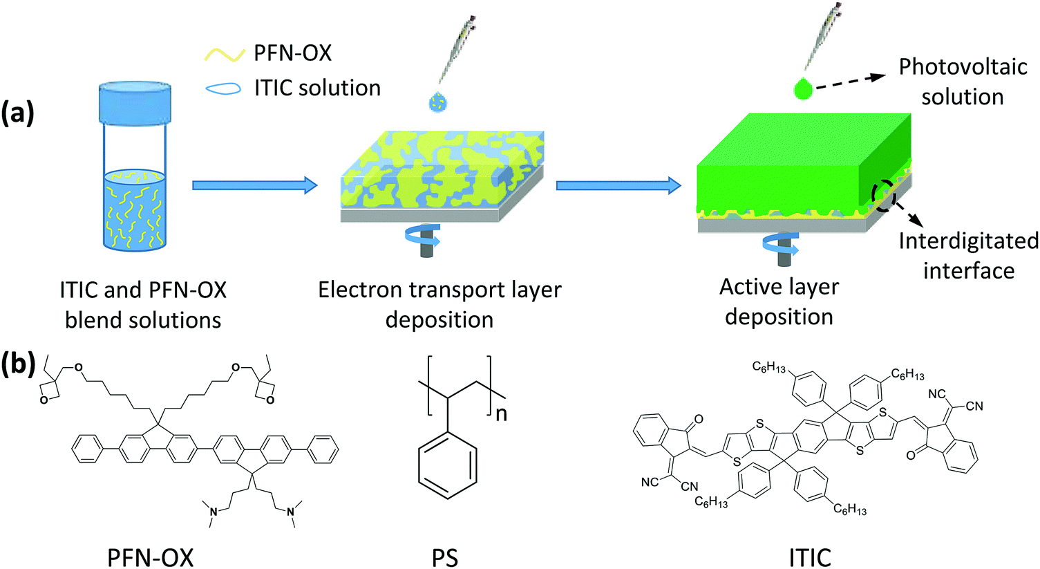 | ||
| Fig. 1 (a) Schematic diagram of the fabrication process of the interdigitated interface between PFN-OX and the photoactive layer via templation. (b) Chemical structures of PFN-OX and the template materials PS and ITIC. | ||
Current density–voltage (J–V) curves under AM 1.5G illumination (100 mW cm−2) were measured with programmable J–V sweep software developed by Ossila Ltd (Sheffield, UK). Before J–V testing, the intensity of the Newport 3A solar simulator was first calibrated with a NREL-certified silicon reference cell. An aperture mask was placed over the devices to accurately define a test area of 2.12 mm2 on each pixel and to eliminate the influence of stray and wave-guided light. The surface morphology was characterized by AFM (NT-MDT, Russia). The absorption of the films was measured with a UV-vis Spectrophotometer (HITACHI, Japan) equipped with an integrating sphere. Film thickness measurements were conducted using a spectroscopic ellipsometer (J. A. Woollam, USA).
3. Results and discussion
The approach to create an interdigitated interface between PFN-OX and the photoactive layer is pictured in Fig. 1. PFN-OX was dissolved in CB with the assistance of a small amount of acetic acid (CB:acetic acid = 100:1). ITIC was dissolved in pure CB and then mixed with the PFN-OX solution. The PFN-OX:ITIC (7.5:92.5, wt%) blend films were then spin cast to form uniform thin films with phase separation between PFN-OX and ITIC occurring during the solvent evaporation process (see Fig. 1a). The photoactive layer was then cast from the CB solution of PTB7-Th:PC71BM photovoltaic blends. The CB solvent can dissolve the ITIC component and take most of the ITIC away during the spin casting process, whilst residual ITIC template materials still remained, with a preferential location in the bulk and bottom regions of the PFN-OX layer. The removal of the ITIC template materials in the surface region of the PFN-OX ETL allowed the permeation of PTB7-Th:PC71BM into the pores to create an interdigitated interface between the photoactive material and PFN-OX.
To characterize the surface porous characteristics of the PFN-OX layer created in situ by the above method (see Fig. 1a), we have investigated the surface topography of a PFN-OX:ITIC blend film (ca. 12.5 nm thick) before and after CB washing. The surface of the pristine ITIC film is extremely smooth with a low RMS of ∼0.2 nm only from scanning probe microscopy (SPM) measurement as shown in Fig. S1a and d (ESI†). This low RMS roughness remains similar to the surface of the PFN-OX:ITIC blend film (Fig. S1b and e, ESI†), suggesting well-mixed PFN-OX and ITIC components during the film drying process. However, surface porous textures were created after the ITIC component was washed away by rinsing the blend film with CB (the same volume as that used to spin cast the photoactive layer). Pores can be observed on the film surface in Fig. S1c and f (ESI†), and a comparison has been provided in Fig. 2a. Surface profiles obtained from Fig. 2a are plotted in Fig. 2b, from which pores with an average diameter of 0.23 μm and a depth of 1.1 nm can be seen.
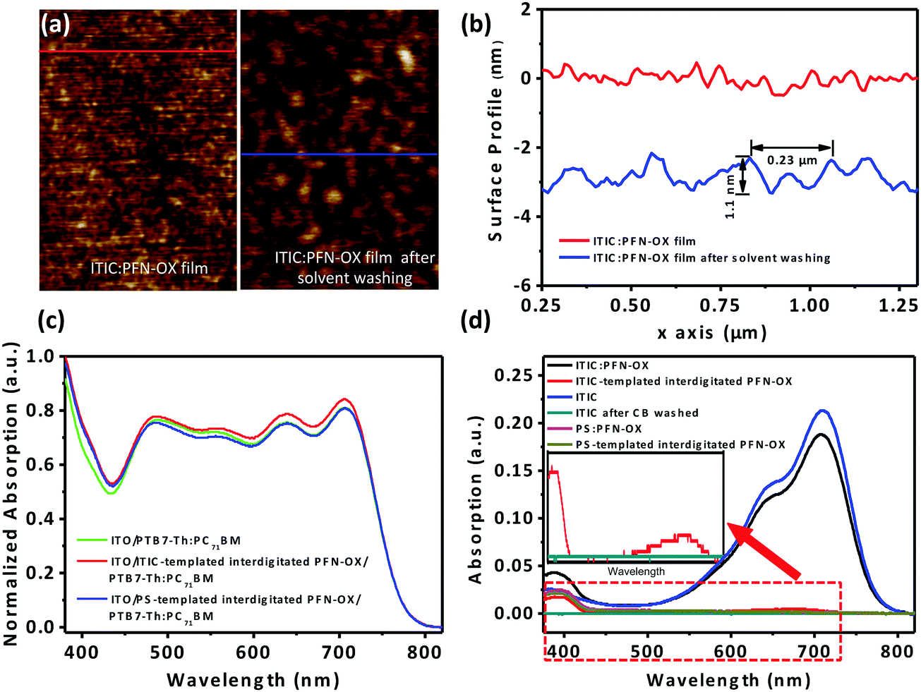 | ||
| Fig. 2 (a) AFM topography of the ITIC:PFN-OX blend film cast on a glass substrate before (left) and after (right) CB wash. Image size 1 μm × 1.5 μm. (b) Corresponding surface topographic profiles. (c) UV-vis absorption spectra of PTB7-Th:PC71BM films cast on different ETLs. (d) Absorption spectra of different ETLs before and after CB rinsing. Inset shows the magnification image in the wavelength region of 400 to 700 nm. | ||
ITIC has a strong light absorption in the wavelength range from 500 to 800 nm, whilst that of PFN-OX has a weak absorption peak at ca. 400 nm.23,24 UV-vis spectra were then obtained to determine whether the ITIC template material had been completely removed during the CB rinsing process. Comparisons were also made by employing an insulating PS as the template material. As shown in Fig. 2d, the PFN-OX:ITIC blend film displays the characteristic absorption of ITIC at 550–750 nm, with another weak peak at 400 nm that is associated with PFN-OX. The PFN-OX:PS shows the absorption peak of PFN-OX at 400 nm only as PS is optically transparent in the wavelength range of visible region.25 After CB rinsing, the absorption peaks at 400 nm were unchanged in PFN-OX:ITIC and PFN-OX:PS films, confirming the existence of PFN-OX. For the pristine ITIC film, the absorption spectrum disappeared completely after CB rinsing as CB is a good solvent for ITIC. The spectrum intensity from the range of 500 to 800 nm was substantially reduced in the PFN-OX:ITIC blend films, suggesting the removal of a large amount of the ITIC component. However, this absorption spectrum still exists (see the inset of Fig. 1c), indicating that residual ITIC still exists, preferentially in the bulk or substrate regions and is harder to remove compared to that in the surface region. Morphological and optical studies therefore confirm the creation of interdigitated PFN-OX ETLs by using ITIC and PS as template materials.
To examine the impact of this PFN-OX ETL having an interdigitated interface with the photoactive layer on device performance, we have fabricated inverted photovoltaic devices using both PTB7-Th:PC71BM and PTB7-Th:ITIC as the photoactive layer. ITIC-templated PFN-OX was chosen as the primary ETL to optimize the performance of the PTB7-Th:PC71BM solar cells. Without the existence of any ETL on the ITO substrate, the maximum efficiency of the PTB7-Th:PC71BM device is terrible at 1.3% only, confirming the necessity for incorporating an ETL to improve electron injection to ITO. When a layer of pristine ITIC was cast onto ITO, the resulting maximum device efficiency was also poor at 1.6%, as this ITIC layer was largely removed during the solution casting process of the photoactive layer (see Fig. 3a and Table 1). By adding only 2.5 wt% PFN-OX into ITIC, the maximum device efficiency can be dramatically increased to 7.6% (see Fig. S2a, ESI†). The device efficiency can be further improved by increasing the PFN-OX content into ITIC, with the optimized ratio of PFN-OX:ITIC determined to be 7.5:92.5 (wt%). This led to a maximum PCE of 10.4%, together with a Jsc of 18.5 mA cm−2, a Voc of 0.77 and a FF of 72.6%. The maximum achievable device PCE reduced slightly when the content of PFN-OX in the blend films increased further. More importantly, the device efficiency is largely insensitive to the thickness of this ITIC-templated PFN-OX ETL (see Fig. S2b, ESI†) although the optimal thickness is ca. 12.5 nm. This is of significant merit compared to the planar PFN-OX ETL, whose thickness has to be limited to a few nanometers due to its relatively low electrical conductivity. The PTB7-Th:PC71BM solar cells employing a PS-templated interdigitated PFN-OX ETL also achieved an enhanced maximum device PCE of 9.9%, a value that is much higher than that of 9.3% for the device incorporating a planar and pristine PFN-OX ETL. The PFN-OX/ITIC bilayer was also coated on an ITO substrate, followed by the casting of the PTB7-Th:PC71BM photoactive layer and MoO3/Ag via thermal evaporation to fabricate device ITO/PFN-OX/ITIC/PTB7-Th:PC71BM/MoO3/Ag, and we found that the device efficiency was 9.3%. This value is close to the PCE incorporating a planar and pristine PFN-OX ETL, as the ITIC layer will be washed out during the casting process of PTB7-Th:PC71BM.
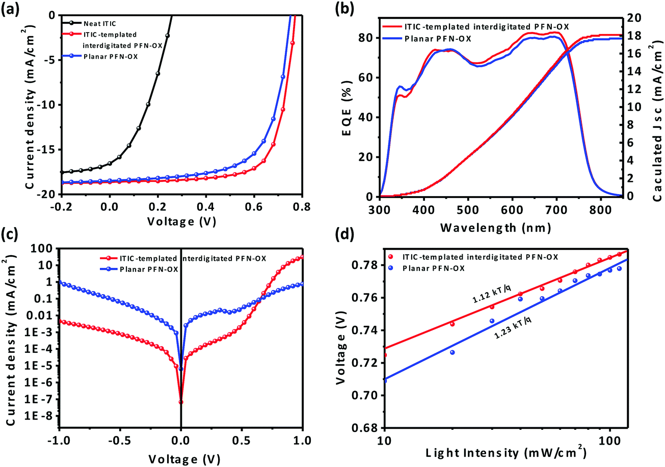 | ||
| Fig. 3 (a) Champion J–V curves, (b) EQE spectra, (c) dark J–V curves, and (d) light-intensity dependent open-circuit voltage of PTB7-Th:PC71BM solar cells employing planar and ITIC-templated interdigitated PFN-OX ETLs. | ||
| ETLs | Active layer | PCEmax (PCEave) (%) | FF (%) | J sc (mA cm−2) | V oc (V) |
|---|---|---|---|---|---|
| — | PTB7-Th:PC71BM | 1.3 (1.3 ± 0.1) | 36.7 (36.0 ± 0.7) | −16.2 (−16.6 ± 0.4) | 0.22 (0.22 ± 0.01) |
| ITIC | PTB7-Th:PC71BM | 1.6 (1.5 ± 0.1) | 37.3 (36.2 ± 0.8) | −16.0 (−16.4 ± 0.2) | 0.26 (0.25 ± 0.01) |
| Planar PFN-OX | PTB7-Th:PC71BM | 9.3 (9.1 ± 0.1) | 67.1 (66.5 ± 0.4) | −18.2 (−18.1 ± 0.1) | 0.76 (0.76 ± 0.0) |
| ITIC-templated interdigitated PFN-OX | PTB7-Th:PC71BM | 10.4 (10.2 ± 0.1) | 72.6 (71.5 ± 1.0) | −18.5 (−18.6 ± 0.2) | 0.77 (0.77 ± 0.0) |
| PS-templated interdigitated PFN-OX | PTB7-Th:PC71BM | 9.9 (9.7 ± 0.1) | 69.4 (68.2 ± 0.7) | −18.3 (−18.6 ± 0.2) | 0.77 (0.77 ± 0.0) |
| Planar PFN-OX | PTB7-Th:ITIC | 7.4 (7.2 ± 0.1) | 58.9 (58.1 ± 0.5) | −16.1 (−15.7 ± 0.2) | 0.78 (0.77 ± 0.01) |
| ITIC-templated interdigitated PFN-OX | PTB7-Th:ITIC | 8.3 (7.9 ± 0.2) | 61.3 (59.8 ± 0.8) | −17.1 (−16.5 ± 0.4) | 0.80 (0.80 ± 0.0) |
In comparison to the planar PFN-OX based device, devices with interdigitated PFN-OX exhibited enhanced Jsc and FF (see Table 1). External quantum efficiency (EQE) measurements confirmed the enhanced Jsc value as illustrated in Fig. 3b. Dark J–V curves from relevant devices are plotted in Fig. 3c to reveal the charge rectification property. The PTB7-Th:PC71BM device based on the planar PFN-OX ETL exhibits a large leakage current, which can be ascribed to the low coverage of PFN-OX on ITO due to an ultrathin (but optimum) thickness of ∼3 nm only. The current leakage can be effectively suppressed by applying a thicker interdigitated PFN-OX ETL. The light-intensity dependent open-circuit voltage plots are shown in Fig. 3d. The planar PFN-OX ETL based device has a higher slope of 1.23kT/q over the 1.12kT/q of the interdigitated PFN-OX ETL based device (where q is the electron charge, k is Boltzmann's constant, and T is the absolute temperature), suggesting slightly increased trap-assisted recombination in the former.26 This interdigitated PFN-OX ETL can also increase the device efficiency of PTB7-Th:ITIC non-fullerene solar cells. A PCE of 8.3% was achieved in the PTB7-Th:ITIC device, together with a Voc of 0.80 V, Jsc of 15.8 mA cm−2 and FF of 61.3% (see in Fig. S3, ESI†). This is superior to the device PCE of 7.4%, together with a Voc of 0.78 V, Jsc of 16.1 mA cm−2 and FF of 58.9% when employing a planar and pristine PFN-OX ETL. Our device study therefore demonstrates the generality of this interdigitated PFN-OX ETL for improving the device efficiency of both fullerene and non-fullerene PSCs.
We have concluded from the absorption spectrum measurements that residual ITIC will remain in the bulk for the bottom region of the interdigitated PFN-OX ETL during the solution casting process of the photoactive layer. We therefore attribute the superior effect of the ITIC-templated PFN-OX ETL over that of the PS-templated PFN-OX ETL (see Table 1) to the electrical doping effect of ITIC on PFN-OX as well as charge transfer between PTB7-Th and ITIC, results that we will discuss in the following section. Previous work has demonstrated the enhanced electrical properties after n-doping electron-acceptors by directly co-dissolving the n-dopant with the electron-acceptor.27–30 Photoluminescence (PL) spectra of pristine ITIC and the PFN-OX:ITIC blend are shown in Fig. 4a. The addition of 7.5 wt% PFN-OX into ITIC dramatically reduced the PL intensity to approximately half of the initial value. We note that this intensity reduction caused by weight loss should be excluded, as only 7.5 wt% ITIC was replaced by PFN-OX. This dramatic PL quenching can be attributed to n-type doping that originated from electron transfer from the amine groups of PFN-OX to ITIC molecules. We have also fabricated bilayer devices to further investigate charge transfer between these organic molecules, with the J–V curves obtained under simulated AM 1.5 sunlight conditions (see Fig. 4b). The bilayer device ITO/PFN-OX/PTB7-Th/MoO3/Ag gave the lowest Jsc of 0.25 mA cm−2, which indicates the negligible charge transfer between PTB7-Th and PFN-OX. The charge transfer between PTB7-Th and ITIC is higher (achieving a Jsc of 0.71 mA cm−2), with the charge transfer between PTB7-Th and ITIC-templated PFN-OX most efficient (achieving a Jsc of 1.29 mA cm−2). We can then conclude that the charge transfer between ITIC:PFN-OX and PTB7-Th is the most efficient compared to that between ITIC (or PFN-OX) and PTB7-Th, a characteristic that will facilitate charge collection in ITIC-templated PFN-OX ETL based devices.
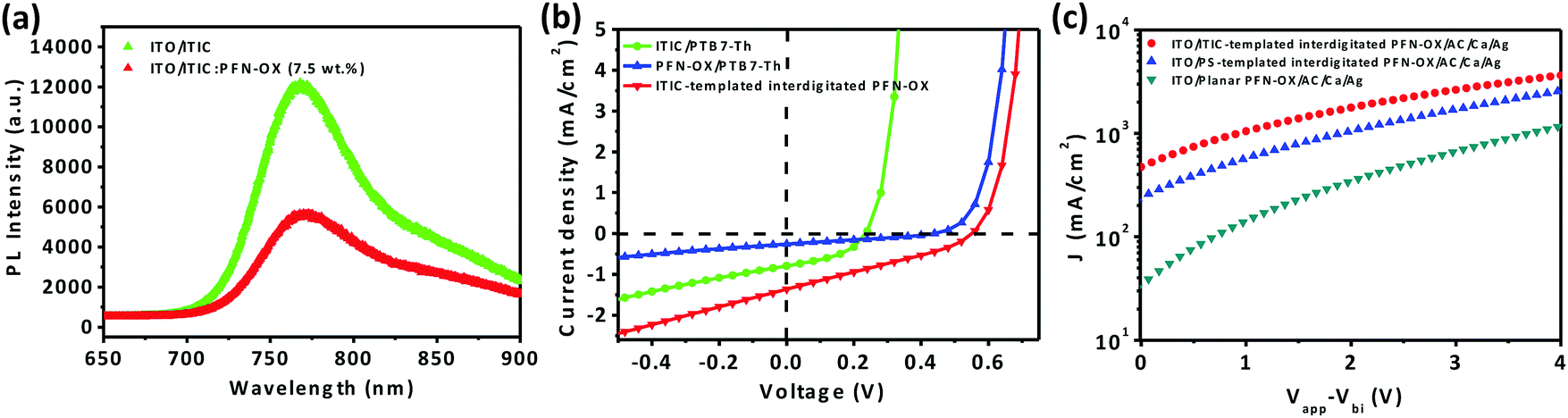 | ||
| Fig. 4 (a) PL spectra of ITIC and ITIC:PFN-OX (7.5 wt%) films cast on ITO. (b) J–V characteristics of bilayer devices ITO/bilayer/MoO3/Ag employing different ETLs. (c) Dark J–V curves of electron-only devices having PFN-OX, PS-templated and ITIC-templated interdigitated PFN-OX as ETLs. | ||
To investigate the electron transport properties of devices with various PFN-OX ETLs, electron-only devices with the configuration of ITO/ETL/PTB7-Th:PC71BM/Ca/Ag were fabricated and the corresponding J–V curves under dark conditions are shown in Fig. 4c. Devices based on the ITIC-templated interdigitated PFN-OX ETL exhibited an enhanced current density compared with that based on the planar PFN-OX ETL.31 Interestingly, devices based on the PS-templated interdigitated PFN-OX ETL also exhibited enhanced current density. These results confirm the improved electron transport of the interdigitated PFN-OX ETL.
Additionally, this interdigitated PFN-OX ETL also enhances the device stability. Our devices have been encapsulated using epoxy and glass slides, and stored in air with an ambient humidity around 40% for a preliminary short period of 300 h when the devices were not being tested. Fig. 5 plots the normalized PCE evolution over storage time. The planar PFN-OX based PTB7-Th:PC71BM device retained ∼93% of its PCE, whilst 97.5% efficiency was retained when the ETL was ITIC-templated interdigitated PFN-OX, which may be attributed to the improved interfacial integration.
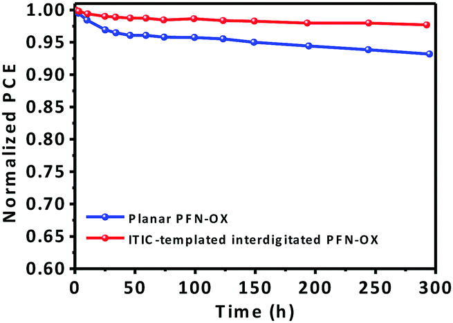 | ||
| Fig. 5 (a) Stability of PTB7-Th:PC71BM solar cells employing planar and ITIC-templated interdigitated PFN-OX ETLs. | ||
4. Conclusion
In summary, we have developed a novel interdigitated PFN-OX ETL templated via either semiconducting ITIC or insulating PS, and have demonstrated its superior characteristics for improving the device and the stability of both fullerene and non-fullerene polymer solar cells. The inverted PTB7-Th:PC71BM solar cell based on ITIC-templated interdigitated PFN-OX ETL achieved a PCE of 10.4% over the 9.3% of the device based on the planar PFN-OX ETL. The PTB7-Th:PC71BM solar cell based on the PS-templated interdigitated PFN-OX ETL can also yield a PCE approaching 10%, which demonstrates the validity of this construction strategy. The PTB7-Th:ITIC non-fullerene solar cells employing this ITIC-templated surface porous PFN-OX ETL received an enhanced PCE from 7.4% to 8.3%. PL and charge transfer study indicated that favorable electrical doping between PFN-OX and ITIC as well as charge transfer between PTB7-Th and ITIC contributed to the enhancement in device performance using the ITIC-templated interdigitated PFN-OX ETL. Our results provide a new strategy to develop a novel electron transport layer to enhance the efficiency and stability of both fullerene and non-fullerene polymer solar cells.Conflicts of interest
There are no conflicts to declare.Acknowledgements
This work was supported by the National Natural Science Foundation of China (Grants no. 21774097, 21504065), and the Natural Science Foundation of Hubei Province (Grants no. 2018CFA055). T. W. acknowledges support from the Recruitment Program of Global Experts (1000 Talents Plan) of China.References
- S. Q. Zhang, Y. P. Qin, J. Zhu and J. H. Hou, Adv. Mater., 2018, 30, 1800868 CrossRef PubMed.
- S. S. Li, L. Ye, W. C. Zhao, H. P. Yan, B. Yang, D. L. Liu, W. N. Li, H. Ade and J. H. Hou, J. Am. Chem. Soc., 2018, 140, 7159–7167 CrossRef PubMed.
- X. Z. Che, Y. X. Li, Y. Qu and S. R. Forrest, Nat. Energy, 2018, 3, 422–427 CrossRef.
- W. C. Zhao, S. S. Li, H. F. Yao, S. Q. Zhang, Y. Zhang and J. H. Hou, J. Am. Chem. Soc., 2017, 139, 7148–7151 CrossRef PubMed.
- J. B. Zhao, Y. K. Li, G. F. Yang, K. Jiang, H. R. Lin, H. Ade, W. Ma and H. Yan, Nat. Energy, 2016, 1, 15027 CrossRef.
- Y. Cui, H. F. Yao, B. W. Gao, Y. P. Qin, S. Q. Zhang, B. Yang, C. He, B. W. Xu and J. H. Hou, J. Am. Chem. Soc., 2017, 139, 7302–7309 CrossRef PubMed.
- Z. C. He, C. M. Zhong, S. J. Su, M. Xu, H. B. Wu and Y. Cao, Nat. Photonics, 2012, 6, 593–597 Search PubMed.
- S. H. Liao, H. J. Jhuo, Y. S. Chen and S. A. Chen, Adv. Mater., 2013, 25, 4766–4771 CrossRef PubMed.
- X. G. Guo, N. J. Zhou, S. J. Lou, J. Smith, D. B. Tice, J. W. Hennek, R. P. Ortiz, J. T. L. Navarrete, S. Y. Li, J. Strzalka, L. X. Chen, R. P. H. Chang, A. Facchetti and T. J. Marks, Nat. Photonics, 2013, 7, 825–833 CrossRef.
- K. Wang, C. Liu, T. Y. Meng, C. Yi and X. Gong, Chem. Soc. Rev., 2016, 45, 2937 RSC.
- Y. M. Sun, J. H. Seo, C. J. Takacs, J. Seifter and A. J. Heeger, Adv. Mater., 2011, 23, 1679–1683 CrossRef PubMed.
- Y. Yan, F. L. Cai, L. Y. Yang, W. Li, Y. Y. Gong, J. L. Cai, S. Liu, R. S. Gurney, D. Liu and T. Wang, ACS Appl. Mater. Interfaces, 2017, 9, 32678–32687 CrossRef PubMed.
- A. Sundqvist, O. J. Sandberg, M. Nyman, J. H. Smått and R. Österbacka, Adv. Energy Mater., 2016, 6, 1502265 CrossRef.
- Y. Yan, F. L. Cai, L. Y. Yang, J. H. Li, Y. W. Zhang, F. Qin, C. X. Xiong, Y. H. Zhou, D. G. Lidzey and T. Wang, Adv. Mater., 2017, 29, 1604044 CrossRef PubMed.
- D. Son, T. Kuwabara, K. Takahashi and K. Marumoto, Appl. Phys. Lett., 2016, 109, 1434 Search PubMed.
- K. Zhang, Z. C. Hu, C. Sun, Z. H. Wu, F. Huang and Y. Cao, Chem. Mater., 2017, 29, 141–148 CrossRef.
- S. J. Liu, C. M. Zhong, J. Zhang, C. H. Duan, X. H. Wang and F. Huang, Sci. China: Chem., 2011, 54, 1745–1749 CrossRef.
- F. Huang, H. B. Wu, D. L. Wang, W. Yang and Y. Cao, Chem. Mater., 2004, 16, 708–716 CrossRef.
- C. M. Zhong, S. J. Liu, F. Huang, H. B. Wu and Y. Cao, Chem. Mater., 2011, 23, 4870–4876 CrossRef.
- K. A. Bush, A. F. Palmstrom, J. Y. Zhengshan, M. Boccard, R. Cheacharoen, J. P. Mailoa, D. P. McMeekin, R. L. Z. Hoye, C. D. Bailie, T. Leijtens, I. M. Peters, M. C. Minichetti, N. Rolston, R. Prasanna, S. Sofia, D. Harwood, W. Ma, F. Moghadam, H. J. Snaith, T. Buonassisi, Z. C. Holman, S. F. Bent and M. D. McGehee, Nat. Energy, 2017, 2, 17009 CrossRef.
- D. Y. Son, J. W. Lee, Y. J. Choi, I. Jang, S. Lee, P. J. Yoo, H. Shin, N. Ahn, M. Choi, D. Kim and N. G. Park, Nat. Energy, 2016, 1, 16081 CrossRef.
- W. S. Yang, B. W. Park, E. H. Jung, N. J. Jeon, Y. C. Kim, D. U. Lee, S. S. Shin, J. Seo, E. K. Kim, J. H. Noh and S. I. Seok, Science, 2017, 356, 1376–1379 CrossRef PubMed.
- Q. Hu, Y. Liu, Y. Li, L. Ying, T. H. Liu, F. Huang, S. F. Wang, W. Huang, R. Zhu and Q. H. Gong, J. Mater. Chem. A, 2015, 3, 18483 RSC.
- Y. Z. Lin, J. Y. Wang, Z. G. Zhang, H. T. Bai, Y. F. Li, D. B. Zhu and X. W. Zhan, Adv. Mater., 2015, 27, 1170–1174 CrossRef PubMed.
- T. Li, C. L. Zhou and M. Jiang, Poly. Bull., 1991, 25, 211–216 CrossRef.
- C. M. Proctor, M. Kuik and T. Q. Nguyen, Prog. Polym. Sci., 2013, 38, 1941–1960 CrossRef.
- S. Dong, Z. C. Hu, K. Zhang, Q. W. Yin, X. F. Jiang, F. Huang and Y. Cao, Adv. Mater., 2017, 29, 1701507 CrossRef PubMed.
- Z. H. Wu, C. Sun, S. Dong, X. F. Jiang, S. P. Wu, H. B. Wu, H. L. Yip, F. Huang and Y. Cao, J. Am. Chem. Soc., 2016, 138, 2004–2013 CrossRef PubMed.
- C. Z. Li, C. C. Chueh, F. Z. Ding, H. L. Yip, P. W. Liang, X. S. Li and A. K. Y. Jen, Adv. Mater., 2013, 25, 4425–4430 CrossRef PubMed.
- N. Cho., H. L. Yip, J. A. Davies, P. D. Kazarinoff, D. F. Zeigler, M. M. Durban, Y. Segawa, K. M. O'Malley, C. K. Luscombe and A. K. Y. Jen, Adv. Energy Mater., 2011, 1, 1148–1153 CrossRef.
- X. H. Ouyang, R. X. Peng, L. Ai, X. Y. Zhang and Z. Y. Ge, Nat. Photonics, 2015, 9, 520 CrossRef.
Footnote |
| † Electronic supplementary information (ESI) available. See DOI: 10.1039/c8qm00347e |
| This journal is © the Partner Organisations 2018 |