
Effects of different types of unsymmetrical squaraines on the material properties and Coulomb interactions in organic photovoltaic devices†
Lin
Yang‡
 ab,
Daobin
Yang‡
ac,
Yao
Chen
a,
Jianglin
Wu
a,
Zhiyun
Lu
a,
Hisahiro
Sasabe
c,
Junji
Kido
c,
Takeshi
Sano
c and
Yan
Huang
*a
ab,
Daobin
Yang‡
ac,
Yao
Chen
a,
Jianglin
Wu
a,
Zhiyun
Lu
a,
Hisahiro
Sasabe
c,
Junji
Kido
c,
Takeshi
Sano
c and
Yan
Huang
*a
aKey Laboratory of Green Chemistry and Technology (Ministry of Education), College of Chemistry, Sichuan University, Chengdu 610064, P. R. China. E-mail: huangyan@scu.edu.cn
bDepartment of Medicinal Chemistry, School of Pharmacy, Southwest Medical University, Luzhou, Sichuan 646000, P. R. China
cDepartment of Organic Materials Science, Research Center for Organic Electronics (ROEL), Frontier Center for Organic Materials (FROM), Yamagata University, Yonezawa, 992-8510, Japan
First published on 21st September 2018
Abstract
Three unsymmetrical squaraine (USQ) dyes bearing different molecular skeletons were employed as donor materials in bulk-heterojunction (BHJ) organic photovoltaics (OPVs). The different molecular skeleton types of the USQs have an influence on their solid-state packing modes, optical properties, frontier orbital energy levels, carrier mobility and photovoltaic performance. More importantly, they also induce distinct differences in the strength of Coulomb interactions between the charge pairs in the USQ and fullerene phases. Through single crystal analysis, film morphology characterization and device architecture investigation with varying thicknesses of a bathocuproine (BCP) layer, it is found: firstly, the photovoltaic performances of the three USQ:PC71BM systems show different sensitivity to different BCP thickness, which can indirectly reflect that Coulomb attractions exist between the USQ phase and electrons in the PC71BM phase; secondly, a low electron mobility (1–2 × 10⁻⁴ cm2 V−1 s−1) in USQ![[thin space (1/6-em)]](https://www.rsc.org/images/entities/char_2009.gif) :PC71BM (1:3) blend films may be attributed to the combination of well-mixed morphologies and strong Coulomb interactions; and thirdly, the USQ structures can affect the intensity of Coulomb attractions between the USQ phase and electrons in the PC71BM phase, and the influence can be large enough to not consider the morphology effect in some cases.
:PC71BM (1:3) blend films may be attributed to the combination of well-mixed morphologies and strong Coulomb interactions; and thirdly, the USQ structures can affect the intensity of Coulomb attractions between the USQ phase and electrons in the PC71BM phase, and the influence can be large enough to not consider the morphology effect in some cases.
1. Introduction
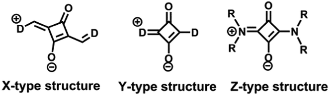
Organic photovoltaics (OPVs) have attracted considerable attention due to their technological potential for cost-effective and scalable production of renewable energy.1–3 Among the various device architectures, bulk-heterojunctions (BHJ) that comprise interpenetrating networks of electron donor (D) and electron acceptor (A) materials have been demonstrated as the most successful ones.1,2,4,5 Although non-fullerene acceptor materials have made great progress in recent years,6–12 most BHJ-OPVs still use fullerene derivatives (e.g. [6,6]-phenyl-C71butyric acid methyl ester (PC71BM) and [6,6]-phenyl-C61butyric acid methyl ester (PC61BM)) as the electron acceptor, and more attention is paid to donor materials.13–17 The vast majority of research has focused on the relationship between molecular structures and their photovoltaic properties, and a remarkable power conversion efficiency (PCE) of over 11% has been achieved for both polymer-based and small molecular-based single-junction BHJ-OPVs through exquisite design of their molecular structure.14,18–20 However, there is still no uniform understanding of some molecular design principles, since the material systems are various and complicated, and the criteria of the system may not necessarily or even counterproductively apply to another. Therefore, an in-depth study of the relationship between molecular structure and photoelectrical performance is still a critical and valuable issue for the rational design of photovoltaic materials.Squaraine dyes (SQs) have emerged as promising donor materials in OPVs due to their strong absorption bands in the visible and near infrared regions, simple synthetic routes, remarkable stability and wide molecular structure diversity.21–26 According to their molecular structure, SQs can be grouped into three general categories illustrated in Scheme 1.21,22,27 These are the corresponding condensation products of squaric acid with appropriate anhydrobases (X-type),28–30 activated arenes or π-excessive heterocycles (Y-type),21,31–34 and primary or secondary amines (Z-type).27,35,36 According to the reported literature,27,37–39 the three types of SQ show very divergent photophysical, chemical, electrical and molecular packing properties. In particular, it has been demonstrated that the electron-deficient central ring of Y-type SQs could be attacked by a nucleophilic reagent,38,40,41 whereas that of the X-type SQs was almost never attacked under the same conditions.38 The different properties of the three types of squaraines also affect their photovoltaic performance. Among the squaraine photovoltaic materials, the Y-type squaraines are the main ones, and show obviously higher PCEs (4–6%) than those of the X-type squaraines (1–2%).22,42 However, there is little systematic research work that unveils the effects of the molecular structures of the three different types of squaraines on their molecular and photovoltaic properties.
 | ||
| Scheme 1 Three types of photovoltaic squaraine dye (D = electron-rich aromatic or heterocyclic rings; R = alkyl or aryl groups). | ||
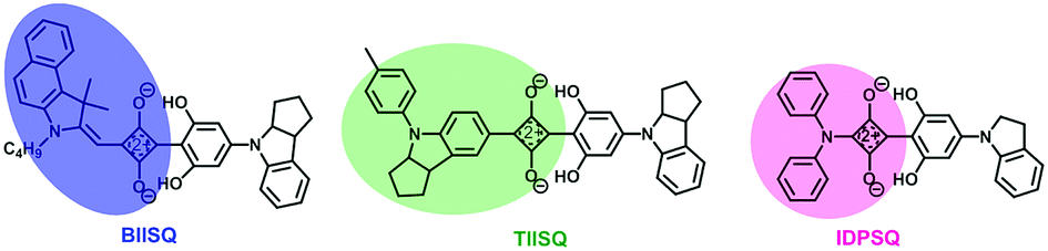
Recently, unsymmetrical squaraines (USQs) have exhibited more promising OPV performances than symmetrical squaraines.23,43 Therefore, in this contribution, three unsymmetrical squaraines (see Scheme 2) with a similar electron-donating group (2,6-dihydroxyphenyl-4-indolinyl derivatives, which exhibited almost the same properties in squaraine-based OPVs44,45), but different types of another donor group, such as a benzoindoly unit46–48 (XY-type, BIISQ), a 4-(p-tolyl)-7-indoly unit34 (YY-type, TIISQ) or a diphenylamine group21,27 (ZY-type, IDPSQ) were synthesized to gain insight into the relationship between their molecular structure and photovoltaic performance.
 | ||
| Scheme 2 Molecular structures of the three objective USQs. | ||
2. Results and discussion
2.1 Synthesis and characterization
The compound BIISQ was synthesized according to the literature.44 The synthetic routes of TIISQ and IDPSQ are outlined in the ESI.† The molecular structures of these USQs were confirmed by 1H NMR, 13C NMR, FT-IR, HR-ESIMS, elemental analysis, and single crystal X-ray diffraction analysis. The high purity of these three USQs (>99.0%) was confirmed via HPLC analysis using tetrahydrofuran/methanol = 1:9 as the eluent. Moreover, all three of the USQs show good solubility in chloroform at room temperature (>15 mg mL−1), which is essential to acquiring smooth and uniform films for OPV applications.
Through crystallographic characterization of the single-crystal samples of the three USQs, the molecular structure information and intermolecular packing modes in the solid state were obtained successfully. As shown in Fig. 1a and Table S1 (ESI†), the common 2,6-dihydroxyphenyl D subunits of the three USQs were found to be different in many aspects including covalent bond length, dihedral angles and hydrogen bond length (O⋯H–O). The dihedral angles between each plane in the π-conjugated structure of these USQs were 0.84° and 9.87° for BIISQ, 0.65° and 14.68° for TIISQ, but 7.34° and 27.16° for IDPSQ, indicating that the molecular backbones of TIISQ and BIISQ are more planar than that of IDPSQ. However, as illustrated in Fig. 1b, TIISQ and IDPSQ display similar antiparallel cofacial stacking structures in their crystal lattices; yet in the case of BIISQ, this displays a slipped anti-parallel stacking structure, despite its relatively planar molecular π-framework. The molecular crystal packing pattern can be affected by a number of factors, and electrostatic potential is one of the most important factors besides the molecular planarity.49,50 As shown in Fig. 1c, the three molecules have a similar electrostatic potential profile along the molecular backbones. However, the negative potentials concentrated on the 2,6-dihydroxyphenyl unit in BIISQ are stronger than that of TIISQ or IDPSQ. More importantly, BIISQ shows the biggest value of positive electrostatic potential among the three USQs (Table S2, ESI†). These results indicate that the repulsive force between the BIISQ molecules is much stronger than that of the TIISQ/IDPSQ molecules. This may trigger stronger Coulomb attractions between BIISQ and the electrons in the PC71BM phases in the BHJ system than that of the other two systems.
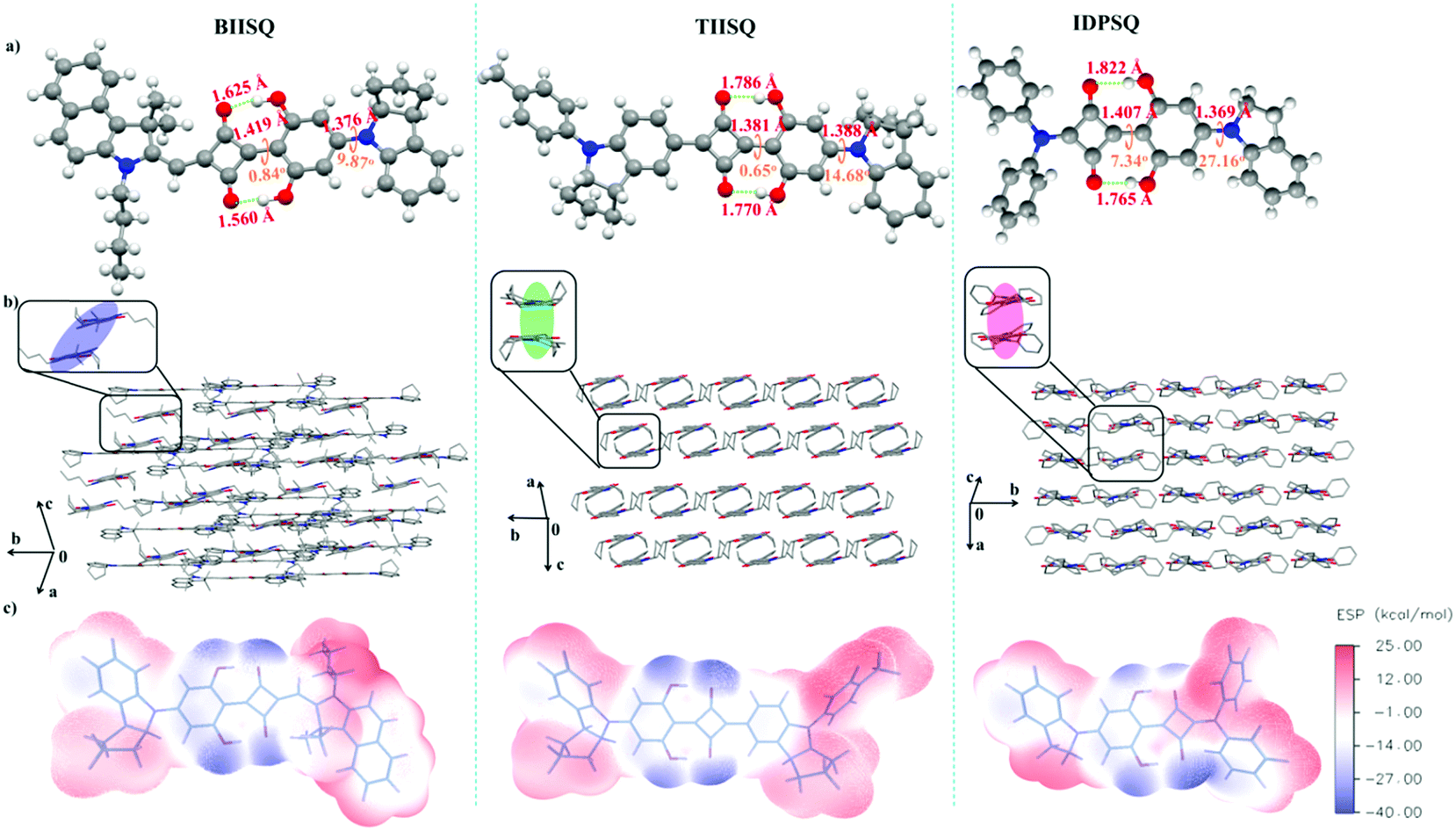 | ||
| Fig. 1 (a) Crystal structures of the USQs, and some important bond lengths and dihedral angles; (b) molecular packing of the single crystals for the USQs; and (c) the electrostatic potential of the USQs plotted on an isodensity surface with the electron density set to 0.001 e bohr−3. | ||
2.2 Optical and electrochemical properties
The UV-vis absorption spectra of the USQs in dilute chloroform solution and thin solid films are shown in Fig. 2, and the relevant data are summarized in Table 1. In the dilute chloroform solution, all of the USQs exhibited a narrow and intense absorption band with the maxima absorption wavelength (λmax) located at 682, 698, and 559 nm, and corresponding molar extinction coefficients of 2.30, 2.37, and 1.01 × 10⁵ L mol−1 cm−1 for BIISQ, TIISQ, and IDPSQ respectively. In thin solid film states, the absorption spectra of all three of the USQs are red-shifted and significantly broadened compared to those of the dilute solution samples, which should be attributed to strong intermolecular interactions within all of the USQs. Through the onset of their absorption spectra in solid-state films, the optical bandgaps of BIISQ (1.56 eV) and TIISQ (1.45 eV) are estimated to be much lower than that of IDPSQ (1.86 eV). | ||
| Fig. 2 UV-vis absorption spectra of the three USQs (a) in chloroform and (b) in thin films. | ||
| USQs | Solution | Film | HOMO [eV] | LUMO [eV] | ||
|---|---|---|---|---|---|---|
| λ max [nm] | ε × 105 [L mol−1 cm−1] | λ max [nm] | E optg [eV] | |||
| BIISQ | 682 | 2.30 | 723 | 1.56 | −5.07 | −3.49 |
| TIISQ | 698 | 2.37 | 749 | 1.45 | −5.11 | −3.65 |
| IDPSQ | 559 | 1.01 | 579 | 1.86 | −5.36 | −3.41 |
The highest occupied molecular orbital (HOMO) and lowest unoccupied molecular orbital (LUMO) energy levels of the three USQs were determined via cyclic voltammetry (CV) measurements (shown in Fig. S1, ESI† and Table 1). The HOMO levels of BIISQ, TIISQ and IDPSQ were estimated to be −5.07 eV, −5.11 eV and −5.36 eV, respectively and the LUMO levels of BIISQ, TIISQ, and IDPSQ were calculated to be −3.49, −3.65, and −3.41 eV, respectively.51
2.3 Photovoltaic characteristics
BHJ-OPV cells with a USQ as the electron donor material and PC71BM as the electron acceptor material were fabricated with the device structure of ITO/MoO3 (8 nm)/USQ:PC71BM (1:3, wt/wt, 60 nm)/bathocuproine (BCP, 6 nm)/Al (100 nm). The corresponding energy level diagram of the device structure is shown in Fig. S2 (ESI†), and the photovoltaic data and curves are shown in Table 2 and Fig. 3. Among the three BHJ-OPV devices, the TIISQ-based one displayed the highest PCE of 4.74% with a Voc of 0.85 V, a Jsc of 11.16 mA cm−2 and an FF of 0.50; the IDPSQ-based one showed a moderate PCE of 4.04% with a Voc of 1.04 V, a Jsc of 9.48 mA cm−2 and an FF of 0.41; and the BIISQ-based one exhibited the worst performance, with a PCE of 3.86%, a Voc of 0.85 V, a Jsc of 9.57 mA cm−2 and an FF of 0.47. A 0.19 V higher Voc of the IDPSQ-based device compared to the other two is consistent with a 0.24 eV lower HOMO energy level of IDPSQ compared to TIISQ and BIISQ; while the differences of these devices with respect to the Jsc and FF should be in connection with the difference in sunlight-capture capability, morphology, and charge-transport mobility of the blend films.
| USQs | C70 [x nm] | BCP [y nm] | V oc [V] | J sc [mA cm−2] | FF | PCEa [%] | R S [Ω cm2] |
|---|---|---|---|---|---|---|---|
| a The average PCE of four devices is shown in parentheses. | |||||||
| BIISQ | 0 | 6 | 0.85 | 9.57 | 0.47 | 3.86 (3.77) | 16 |
| 0 | 10 | 0.85 | 6.45 | 0.22 | 1.23 (1.03) | 264 | |
| 0 | 14 | 0.85 | 3.38 | 0.20 | 0.57 (0.34) | 508 | |
| 0 | 18 | 0.85 | 0.25 | 0.14 | 0.03 (0.02) | 12915 |
|
| 4 | 10 | 0.84 | 9.68 | 0.44 | 3.55 (3.38) | 23 | |
| TIISQ | 0 | 6 | 0.85 | 11.16 | 0.50 | 4.74 (4.65) | 11 |
| 0 | 10 | 0.85 | 10.60 | 0.40 | 3.57 (3.51) | 36 | |
| 0 | 14 | 0.85 | 9.86 | 0.33 | 2.79 (2.34) | 61 | |
| 0 | 18 | 0.85 | 1.90 | 0.16 | 0.26 (0.18) | 1530 | |
| 4 | 10 | 0.84 | 11.95 | 0.44 | 4.47 (4.38) | 20 | |
| IDPSQ | 0 | 6 | 1.04 | 9.48 | 0.41 | 4.04 (3.81) | 24 |
| 0 | 10 | 1.03 | 8.77 | 0.37 | 3.35 (3.27) | 33 | |
| 0 | 14 | 0.95 | 7.00 | 0.30 | 2.01 (1.71) | 79 | |
| 0 | 18 | 1.03 | 1.40 | 0.15 | 0.22 (0.14) | 3422 | |
| 4 | 10 | 1.03 | 8.67 | 0.37 | 3.26 (3.11) | 39 | |
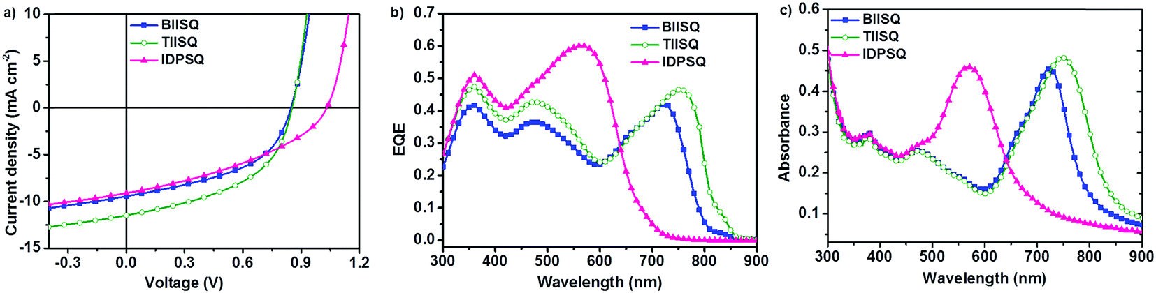 | ||
| Fig. 3 (a) The J–V characteristics of BHJ-OPVs under 100 mW cm−2 simulated AM 1.5G light illumination; (b) the EQE characteristics of the OPV devices; and (c) the absorption spectra based on the blend films of USQ:PC71BM = 1:3. | ||
In-depth investigations of the external quantum efficiency (EQE) curves of the three devices (Fig. 3b) indicated that: despite the narrowest optical responding region (300–700 nm) of IDPSQ, its device showed the highest monochromic light EQE values (0.50–0.60), leading to a moderate Jsc of 9.48 mA cm−2; although the BIISQ-based device showed a lower monochromic light EQE of 0.40–0.45, its responding region is much wider (300–800 nm) than the IDPSQ-device, resulting in a comparable Jsc of 9.57 mA cm−2 with the IDPSQ-based device; and the TIISQ-based device shows the best trade-off between a wide solar light harvesting region (300–850 nm) and a high EQE (0.40–0.50), which could account for its high Jsc of 11.16 mA cm−2. Through a comparison study of the EQE curves of the three devices and the absorption spectra of the corresponding D/A blend films (Fig. 3c), it could be safely deduced that the different optical responding regions of the three devices should originate from the different absorption capabilities of the BHJ active layers.
To gain insight into the reason for the difference in the Jsc and FF of the three devices, atomic force microscopy (AFM) and transmission electron microscopy (TEM) measurements were conducted on the USQ:PC71BM (1:3) blend films to investigate the film morphology. As shown in Fig. 4a–c, all three of the BHJ blend films exhibit a similar smooth surface morphology with a rather small root-mean-square (RMS) roughness (0.17–0.22 nm). However, according to the TEM characterization results (Fig. 4d–f), the IDPSQ:PC71BM blend film possesses the smallest phase separation size among the three BHJ systems. Since squaraine electron donor materials generally suffer from rather short exciton diffusion lengths (2–10 nm),27 the relatively small phase separation size in the BHJ blend film should be propitious to the charge separation procedure at the D/A interfaces, which may account for the comparable Jsc in the IDPSQ- and BIISQ-based devices.52
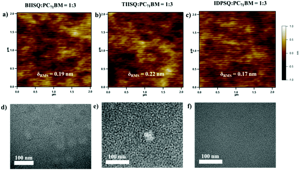 | ||
| Fig. 4 AFM height (2 × 2 μm2), (a–c) and TEM (d–f) images of the USQ:PC71BM = 1:3 blend films. | ||
Additionally, using a space-charge-limited-current (SCLC) method, we measured the hole and electron mobility of the USQ:PC71BM (1:3) blend films (Fig. S3, ESI† and Table 3).53–55 The hole mobility of TIISQ:PC71BM (7.22 × 10⁻⁵ cm2 V−1 s−1) is comparable with that of BIISQ:PC71BM (8.89 × 10⁻⁵ cm2 V−1 s−1), but is much higher than that of IDPSQ:PC71BM (2.95 × 10⁻⁵ cm2 V−1 s−1). However, in the case of electron mobility, the μe of the IDPSQ:PC71BM blend film is calculated to be 2.57 × 10⁻⁴ cm2 V−1 s−1, which is higher than that of TIISQ:PC71BM (1.51 × 10⁻⁴ cm2 V−1 s−1) and BIISQ:PC71BM (1.20 × 10⁻⁴ cm2 V−1 s−1). Through the slope of the J–V curves (Fig. 3a), the series resistance (RS) of the three devices was calculated to be 11, 16, and 24 Ω cm2 for TIISQ-, BIISQ-, and IDPSQ-based devices, respectively (Table 2). Taking into consideration that a relatively low RS often leads to a relatively high FF,56 the lower hole mobility, more unbalanced charge transport capability and the higher RS of the IDPSQ:PC71BM blend film compared to the other two films should be responsible for the lower FF (0.41) of this device compared to the other two devices (FF: 0.47–0.50).57
:PC71BM (1:3) blend films
2.4 The effects of BCP thickness on the photovoltaic performance
BHJ-OPV devices with different BCP thickness were also investigated and the device structure was ITO/MoO3/USQ:PC71BM (1:3)/BCP (6, 10, 14, 18 nm)/Al (shown in Fig. 5a). BCP was selected as a spacer, which is usually inserted between the active layer and the metallic cathode in OPV devices. This protects the active layer from damage due to evaporation of hot cathode metal atoms, and also serves as an exciton blocking layer (EBL).58,59 As depicted in Fig. 5c–f and Table 2, the optimal thickness of the BCP layer for all three of the USQ-based devices was 6 nm. This finding is in line with some reported results that the optimal thickness of the BCP space layer is generally over the range of 2–17 nm.60–66 When the thickness of the BCP layer is increased from 6 to 18 nm, the Voc of all the devices hardly changes, but their Jsc and FF are reduced gradually, leading to a decreased PCE, which may be reasonably attributed to the increased RS of the devices when the BCP thickness is thicker than the optimal one. It is interesting to find that the photovoltaic performances of the USQ-based devices show different degrees of decline with increasing BCP thickness. The PCEs of BIISQ-based devices drop drastically, by 68% from 3.86% (BCP 6 nm) to 1.23% (BCP 10 nm), by 85% to 0.57% (BCP 14 nm), and then to nearly 0 (BCP 18 nm), while the PCEs of the TIISQ-based ones are reduced relatively slowly, by 25% from 4.74% (BCP 6 nm) to 3.57% (BCP 10 nm), by 41% to 2.79% (BCP 14 nm), and then still 0.26% when the BCP thickness is 18 nm. The PCEs of the IDPSQ-based devices are the most gently reduced, by 17% from 4.04% (BCP 6 nm) to 3.35% (BCP 10 nm), by 50% to 2.01% (BCP 14 nm), and then still 0.22% when BCP thickness is 18 nm. In other words, the performance of BIISQ-based devices is much more sensitive to the BCP thickness than that of the TIISQ/IDPSQ-based ones. Additionally, the PCEs of all these devices fall significantly to nearly 0 when the thickness of the BCP layer is 18 nm, which seems to be ascribed to the very huge RS (Table 2).61,67 However, Chen et al. reported that the PCE slightly decreased with an increasing BCP thickness (4.11% for 2 nm, 4.03% for 5 nm, 3.74% for 10 nm, and 3.59% for 20 nm) in BHJ-OPV devices.61 In addition, Huang et al. reported that OPV cells with the device structure ITO/CuPc/C60/BCP (1–10 nm)/Al demonstrated good and comparable photovoltaic performances while the cell with a 20 nm BCP layer showed half of the optimal PCE value.64 Therefore, it could be inferred that when the BCP layer is thinner than 20 nm, the increase in RS is not enough to reduce the PCEs of the three USQ-based systems to nearly 0. So what causes the various degrees of decline in the photovoltaic performance of the three USQ-based devices with the increasing thickness of the BCP layer? What makes the photovoltaic performance of the three USQ-based devices almost 0 when the BCP thickness is only 18 nm? We try to explain these experimental results.
 | ||
| Fig. 5 The different configurations of the BHJ-OPV devices (a and b) and the corresponding photovoltaic performance (c–f) under 100 mW cm−2 simulated AM 1.5G light illumination. | ||
In BHJ systems, the excitons are dissociated to form holes and electrons at the D/A interface. The holes and electrons are transported through the donor phase and the acceptor phase respectively to the anode and cathode, and the electron is passed through the BCP layer. In much of the literature, it is thought that the electrons transferred in the acceptor phase (such as PC71BM) after dissociation are “free”.68,69 If the electrons transported in the acceptor phases are absolutely “free”, we think that they should have the strongest ability to pass through the BCP layer. So for different donor systems (D1 or D2), as shown in Fig. 6a, as long as their acceptor material is the same (such as PC71BM), regardless of whether their BHJ morphology is similar or not, the electrons in these two systems (D1:PC71BM and D2:PC71BM) will have the same ability to pass through the same thickness of BCP. Then, the PCEs of the OPV devices should show similar degrees of decline with an increased BCP thickness for these two systems. Obviously, this is not consistent with our experimental results above, which indicate that the electrons transported in the PC71BM phase are not really “free”, but are bound to a certain extent. We speculate that the binding force comes mainly from Coulomb attractions between the donor phase and electrons in the PC71BM phase. If there are Coulomb attractions in these two systems (Fig. 6b), the ability of electrons to pass through the space layer will be weakened. As the Coulomb attractions are stronger, the ability is weaker, thus the PCE of the corresponding OPV devices will show higher degrees of decline with increasing thickness of the BCP layer.
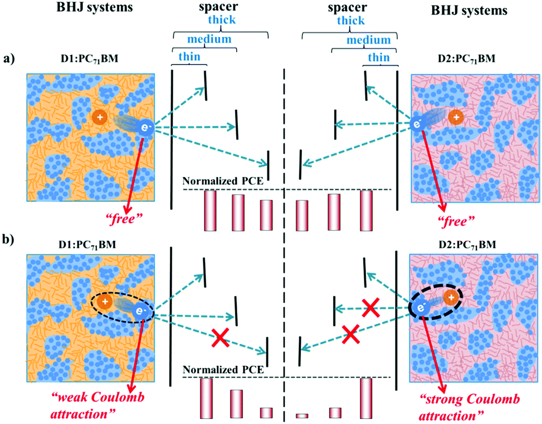 | ||
| Fig. 6 The BHJ-OPV devices based on different donor materials (D1 or D2) and PC71BM with thin, medium or thick space layers. (a) The electrons are “free”; and (b) the electrons are attracted by the different intensity of Coulomb interactions. | ||
Therefore, it could be seen that the photovoltaic performances of USQ-based devices show different degrees of decline with the increasing thickness of the BCP layer, confirming that Coulomb attractions exist between the donor phase and electrons in the PC71BM phase. Moreover, the Coulomb attractions between the BIISQ phase and the PC71BM phase should be stronger than those of IDPSQ and TIISQ BHJ systems. This deduction is further confirmed by the electron mobility data of these blend systems when the BCP layers have a thickness of 6 and 10 nm (Table 3). When the thickness of the BCP layer varies from 6 nm to 10 nm, the BIISQ-based device shows a more reduced electron mobility (1.20 × 10⁻⁴vs. 3.36 × 10⁻⁷ cm2 V−1 s−1) than that of the TIISQ- and IDPSQ-based devices (1.51 × 10⁻⁴vs. 1.29 × 10⁻⁶ cm2 V−1 s−1 for TIISQ, and 2.57 × 10⁻⁴vs. 2.29 × 10⁻⁶ cm2 V−1 s−1 for IDPSQ). This is consistent with the previous deductions from the single crystal and electrostatic potential analysis. Additionally, Coulomb interactions follow an inverse-square law. However, combining the results of TEM and the BCP thickness experiments, the IDPSQ system with a small domain size exhibits smaller Coulomb attraction intensity than the BIISQ system with a middle domain size, and shows a similar Coulomb attraction intensity to the TIISQ system with a relatively large domain size. This demonstrates that the different structures of the three USQs can induce significant differences in the strength of Coulomb interactions in their BHJ systems, so that sometimes the influence is enough large to not consider the morphology effect.
It is also rational to deduce that the Coulomb attractions between the USQ phases and electrons in the PC71BM phases are very strong, which could prevent the electrons from passing through the BCP layer even at a thickness of 18 nm, therefore leading to a nearly undetectable efficiency. Meanwhile, the well-mixed BHJ morphology, combined with the strong Coulomb attractions, are the important reasons that the USQ BHJ systems exhibit a rather low electron mobility (1.20–2.57 × 10⁻⁴ cm2 V−1 s−1) even at a relatively high PC71BM composition of 75 wt% when the BCP is 6 nm.
Additionally, several reports in the literature have unveiled that the hole–electron pairs could become effectively free once they are separated by ∼4 nm,70–73 and we conjecture that the strength of Coulomb interactions should be drastically weakened in the range of 4 nm. Therefore, if a thin layer of a pure electron acceptor material is inserted between the BHJ active layer and the space layer, the electrons can be divorced from the Coulomb attractive bounds before they go through the BCP layer, hence the difference in the OPV performance triggered by Coulomb interactions should be diminished drastically. To validate these inferences, we fabricated three reference devices bearing an additional 4 nm C70 layer between the active layer and a 10 nm BCP space layer (Fig. 5b). Excitingly, the PCEs of all of these reference devices are discovered to be comparable with those devices bearing a 6 nm BCP layer (Fig. 5c–f and Table 2), validating that the presence of relatively strong Coulomb attractions between the USQ phases and the PC71BM phases should be responsible for the sensitivity of these devices toward the thickness of the BCP layer.
3. Conclusions
Three USQs with different types of structure were synthesized. The different types of structure have an effective influence on their solid-state packing, optical properties, energy levels, carrier mobility and photovoltaic performance. Consequently, TIISQ with a YY-type structure exhibits the most excellent performance with a PCE of 4.74%. For IDPSQ with the ZY-type structure, despite its decreasing extent of π-conjugation systems resulting in a blue-shift absorption spectrum, the lowest HOMO level (−5.36 eV) combined with the most optimized phase separation size in the blend film contribute to the second highest PCE of 4.04% for the BHJ-OPV devices. Meanwhile, for BIISQ with the XY-type structure, a moderate PCE of 3.86% was obtained. More importantly, the photovoltaic performances of the USQ-based devices show different degrees of decline with the increasing thickness of the BCP layer, confirming that Coulomb attractions exist between the donor phase and electrons in the PC71BM phase. The USQ-based BHJ morphologies are well-mixed and the Coulomb interactions in the BHJ-OPVs are very strong, which result in a rather low electron mobility (1–2 × 10⁻⁴ cm2 V−1 s−1) in their BHJ layers even at a very high PC71BM composition (75 wt%). The IDPSQ system with a small domain size exhibits a smaller Coulomb attraction strength than the BIISQ system with a middle domain size, and shows a similar Coulomb attraction strength to the TIISQ system with a relatively large domain size. This demonstrates that the different structures of the three USQs can induce significant differences in the strength of the Coulomb interaction, so that sometimes the influence is enough large to not consider the morphology effect. Therefore, when designing novel donor materials, generally, optical property, energy levels, carrier mobility and film morphology are necessary factors to consider, and according to our experimental results, it was found that the Coulomb interactions in the BHJ systems should be another important factor to be considered, whether the acceptor material is a fullerene derivative or nonfullerene.Conflicts of interest
There are no conflicts to declare.Acknowledgements
We acknowledge the financial support for this work from the National Natural Science Foundation of China (project no. 51573108 and 21672156). We are grateful to the Comprehensive Training Platform of Specialized Laboratory, College of Chemistry, Sichuan University for providing NMR, FT-IR, HR-MS, elemental analysis and single crystal diffraction tests. We also would like to thank Dr Peng Wu and Dr Shanling Wang of the Analytical & Testing Center, Sichuan University, for their help in photo-physical measurements and TEM measurements, respectively.Notes and references
- Y. Huang, E. J. Kramer, A. J. Heeger and G. C. Bazan, Chem. Rev., 2014, 114, 7006–7043 CrossRef CAS PubMed.
- A. J. Heeger, Adv. Mater., 2014, 26, 10–28 CrossRef CAS PubMed.
- A. Polman, M. Knight, E. C. Garnett, B. Ehrler and W. C. Sinke, Science, 2016, 352, aad4424 CrossRef PubMed.
- K. Zhang, Z. Hu, C. Sun, Z. Wu, F. Huang and Y. Cao, Chem. Mater., 2017, 29, 141–148 CrossRef CAS.
- S. D. Collins, N. A. Ran, M. C. Heiber and T. Q. Nguyen, Adv. Energy Mater., 2017, 7, 1602242 CrossRef.
- H. Yao, L. Ye, J. Hou, B. Jang, G. Han, Y. Cui, G. M. Su, C. Wang, B. Gao, R. Yu, H. Zhang, Y. Yi, H. Y. Woo, H. Ade and J. Hou, Adv. Mater., 2017, 29, 1700254 CrossRef PubMed.
- W. Zhao, S. Li, H. Yao, S. Zhang, Y. Zhang, B. Yang and J. Hou, J. Am. Chem. Soc., 2017, 139, 7148–7151 CrossRef CAS PubMed.
- W. Li, H. Yao, H. Zhang, S. Li and J. Hou, Chem. – Asian J., 2017, 12, 2160–2171 CrossRef CAS PubMed.
- S. Dai, F. Zhao, Q. Zhang, T. K. Lau, T. Li, K. Liu, Q. Ling, C. Wang, X. Lu, W. You and X. Zhan, J. Am. Chem. Soc., 2017, 139, 1336–1343 CrossRef CAS PubMed.
- J. Wang, W. Wang, X. Wang, Y. Wu, Q. Zhang, C. Yan, W. Ma, W. You and X. Zhan, Adv. Mater., 2017, 29, 1702125 CrossRef PubMed.
- D. Xie, T. Liu, W. Gao, C. Zhong, L. Huo, Z. Luo, K. Wu, W. Xiong, F. Liu, Y. Sun and C. Yang, Sol. RRL, 2017, 1, 1700044 CrossRef.
- X. Zhan, W. Xiong, Y. Gong, T. Liu, Y. Xie, Q. Peng, Y. Sun and Z. Li, Sol. RRL, 2017, 1, 1700123 CrossRef.
- D. Deng, Y. Zhang, J. Zhang, Z. Wang, L. Zhu, J. Fang, B. Xia, Z. Wang, K. Lu, W. Ma and Z. Wei, Nat. Commun., 2016, 7, 13740 CrossRef CAS PubMed.
- B. Kan, M. Li, Q. Zhang, F. Liu, X. Wan, Y. Wang, W. Ni, G. Long, X. Yang, H. Feng, Y. Zuo, M. Zhang, F. Huang, Y. Cao, T. P. Russell and Y. Chen, J. Am. Chem. Soc., 2015, 137, 3886–3893 CrossRef CAS PubMed.
- V. Gupta, L. F. Lai, R. Datt, S. Chand, A. J. Heeger, G. C. Bazan and S. P. Singh, Chem. Commun., 2016, 52, 8596–8599 RSC.
- H. Zhang, S. Zhang, K. Gao, F. Liu, H. Yao, B. Yang, C. He, T. P. Russell and J. Hou, J. Mater. Chem. A, 2017, 5, 10416–10423 RSC.
- Y. Cai, L. Huo and Y. Sun, Adv. Mater., 2017, 29, 1605437 CrossRef PubMed.
- J. Zhao, Y. Li, G. Yang, K. Jiang, H. Lin, H. Ade, W. Ma and H. Yan, Nat. Energy, 2016, 1, 15027 CrossRef CAS.
- W. Zhao, D. Qian, S. Zhang, S. Li, O. Inganas, F. Gao and J. Hou, Adv. Mater., 2016, 28, 4734–4739 CrossRef CAS PubMed.
- J. Wan, X. Xu, G. Zhang, Y. Li, K. Feng and Q. Peng, Energy Environ. Sci., 2017, 10, 1739–1745 RSC.
- S. Wang, L. Hall, V. V. Diev, R. Haiges, G. Wei, X. Xiao, P. I. Djurovich, S. R. Forrest and M. E. Thompson, Chem. Mater., 2011, 23, 4789–4798 CrossRef CAS.
- G. Chen, H. Sasabe, T. Igarashi, Z. Hong and J. Kido, J. Mater. Chem. A, 2015, 3, 14517–14534 RSC.
- Y. Chen, J. Wu, L. Yang, B. Hu, D. Yang, Z. Lu and Y. Huang, Chem. – Eur. J., 2018, 24, 8747–8750 CrossRef CAS PubMed.
- G. Chen, H. Sasabe, Z. Wang, X. F. Wang, Z. Hong, Y. Yang and J. Kido, Adv. Mater., 2012, 24, 2768–2773 CrossRef CAS PubMed.
- G. Chen, H. Sasabe, Y. Sasaki, H. Katagiri, X. F. Wang, T. Sano, Z. Hong, Y. Yang and J. Kido, Chem. Mater., 2014, 26, 1356–1364 CrossRef CAS.
- G. Chen, C. Si, P. Zhang, B. Wei, J. Zhang, Z. Hong, H. Sasabe and J. Kido, Org. Electron., 2017, 51, 62–69 CrossRef CAS.
- G. Wei, X. Xiao, S. Wang, K. Sun, K. J. Bergemann, M. E. Thompson and S. R. Forrest, ACS Nano, 2012, 6, 972–978 CrossRef CAS PubMed.
- B. Fan, Y. Maniglio, M. Simeunovic, S. Kuster, T. Geiger, R. Hany and F. Nüesch, Int. J. Photoenergy, 2009, 2009, 581068 CrossRef.
- U. Mayerhoffer, K. Deing, K. Gruss, H. Braunschweig, K. Meerholz and F. Wurthner, Angew. Chem., Int. Ed., 2009, 48, 8776–8779 CrossRef PubMed.
- B. A. Rao, K. Yesudas, G. S. Kumar, K. Bhanuprakash, V. J. Rao, G. D. Sharma and S. P. Singh, Photochem. Photobiol. Sci., 2013, 12, 1688–1699 RSC.
- H. Sasabe, T. Igrashi, Y. Sasaki, G. Chen, Z. Hong and J. Kido, RSC Adv., 2014, 4, 42804–42807 RSC.
- D. Bagnis, L. Beverina, H. Huang, F. Silvestri, Y. Yao, H. Yan, G. A. Pagani, T. J. Marks and A. Facchetti, J. Am. Chem. Soc., 2010, 132, 4074–4075 CrossRef CAS PubMed.
- Y. Chen, Y. Zhu, D. Yang, Q. Luo, L. Yang, Y. Huang, S. Zhao and Z. Lu, Chem. Commun., 2015, 51, 6133–6136 RSC.
- L. Yang, D. Yang, Y. Chen, Q. Luo, M. Zhang, Y. Huang, Z. Lu, H. Sasabe and J. Kido, RSC Adv., 2016, 6, 1877–1884 RSC.
- Y. Ohsedo, M. Miyamoto, A. Tanaka and H. Watanabe, Dyes Pigm., 2014, 101, 261–269 CrossRef CAS.
- Y. Ohsedo, K. Saruhashi and H. Watanabe, Dyes Pigm., 2015, 122, 134–138 CrossRef CAS.
- C. Gude and W. Rettig, J. Phys. Chem. A, 2000, 104, 8050–8057 CrossRef CAS.
- I. A. Karpenko, A. S. Klymchenko, S. Gioria, R. Kreder, I. Shulov, P. Villa, Y. Mély, M. Hibert and D. Bonnet, Chem. Commun., 2015, 51, 2960–2963 RSC.
- P. F. Santos, L. V. Reis, P. Almeida and D. E. Lynch, CrystEngComm, 2011, 13, 1333–1338 RSC.
- P. Anees, S. Sreejith and A. Ajayaghosh, J. Am. Chem. Soc., 2014, 136, 13233–13239 CrossRef CAS PubMed.
- G. Saranya, P. Anees, M. M. Joseph, K. K. Maiti and A. Ajayaghosh, Chem. – Eur. J., 2017, 23, 7191–7195 CrossRef CAS PubMed.
- C. Si, G. Chen and B. Wei, Chin. J. Org. Chem., 2016, 36, 2602–2618 CrossRef CAS.
- J. Wu, C. Si, Y. Chen, L. Yang, B. Hu, G. Chen, Z. Lu and Y. Huang, Chem. – Eur. J., 2018, 24, 3234–3240 CrossRef CAS PubMed.
- L. Yang, Q. Yang, D. Yang, Q. Luo, Y. Zhu, Y. Huang, S. Zhao and Z. Lu, J. Mater. Chem. A, 2014, 2, 18313–18321 RSC.
- D. Yang, Q. Yang, L. Yang, Q. Luo, Y. Chen, Y. Zhu, Y. Huang, Z. Lu and S. Zhao, Chem. Commun., 2014, 50, 9346–9348 RSC.
- D. Yang, Q. Yang, L. Yang, Q. Luo, Y. Huang, Z. Lu and S. Zhao, Chem. Commun., 2013, 49, 10465–10467 RSC.
- D. Yang, Y. Jiao, L. Yang, Y. Chen, S. Mizoi, Y. Huang, X. Pu, Z. Lu, H. Sasabe and J. Kido, J. Mater. Chem. A, 2015, 3, 17704–17712 RSC.
- D. Yang, Y. Jiao, L. Yang, Q. Yang, Q. Luo, X. Pu, Y. Huang, S. Zhao and Z. Lu, RSC Adv., 2015, 5, 20724–20733 RSC.
- J. H. Dou, Y. Q. Zheng, Z. F. Yao, T. Lei, X. Shen, X. Y. Luo, Z. A. Yu, S. D. Zhang, G. Han, Z. Wang, Y. Yi, J. Y. Wang and J. Pei, Adv. Mater., 2015, 27, 8051–8055 CrossRef CAS PubMed.
- J. H. Dou, Y. Q. Zheng, Z. F. Yao, Z. A. Yu, T. Lei, X. Shen, X. Y. Luo, J. Sun, S. D. Zhang, Y. F. Ding, G. Han, Y. Yi, J. Y. Wang and J. Pei, J. Am. Chem. Soc., 2015, 137, 15947–15956 CrossRef CAS PubMed.
- J. Wu, D. Yang, Q. Wang, L. Yang, H. Sasabe, T. Sano, J. Kido, Z. Lu and Y. Huang, J. Mater. Chem. A, 2018, 6, 5797–5806 RSC.
- M. Li, F. Liu, X. Wan, W. Ni, B. Kan, H. Feng, Q. Zhang, X. Yang, Y. Wang, Y. Zhang, Y. Shen, T. P. Russell and Y. Chen, Adv. Mater., 2015, 27, 6296–6302 CrossRef CAS PubMed.
- V. D. Mihailetchi, J. K. J. van Duren, P. W. M. Blom, J. C. Hummelen, R. A. J. Janssen, J. M. Kroon, M. T. Rispens, W. J. H. Verhees and M. M. Wienk, Adv. Funct. Mater., 2003, 13, 43–46 CrossRef CAS.
- H. Azimi, A. Senes, M. C. Scharber, K. Hingerl and C. J. Brabec, Adv. Energy Mater., 2011, 1, 1162–1168 CrossRef CAS.
- Q. Yang, D. Yang, S. Zhao, Y. Huang, Z. Xu, X. Liu, W. Gong, X. Fan, Q. Huang and X. Xu, Appl. Surf. Sci., 2013, 284, 849–854 CrossRef CAS.
- M. H. Jao, H. C. Liao and W. F. Su, J. Mater. Chem. A, 2016, 4, 5784–5801 RSC.
- C. M. Proctor, J. A. Love and T. Q. Nguyen, Adv. Mater., 2014, 26, 5957–5961 CrossRef CAS PubMed.
- B. P. Rand, J. Li, J. Xue, R. J. Holmes, M. E. Thompson and S. R. Forrest, Adv. Mater., 2005, 17, 2714–2718 CrossRef CAS.
- H. Gommans, B. Verreet, B. P. Rand, R. Muller, J. Poortmans, P. Heremans and J. Genoe, Adv. Funct. Mater., 2008, 18, 3686–3691 CrossRef CAS.
- Z. H. Kafafi, P. A. Lane, I. D. W. Samuel, N. Mendil, M. Daoudi, Z. Berkai and A. Belghachi, Proc. SPIE, 2015, 9567, 956724 CrossRef.
- C. C. Chang, C. F. Lin, J. M. Chiou, T. H. Ho, Y. Tai, J. H. Lee, Y. F. Chen, J. K. Wang, L. C. Chen and K. H. Chen, Appl. Phys. Lett., 2010, 96, 263506 CrossRef.
- P. Peumans and S. R. Forrest, Appl. Phys. Lett., 2001, 79, 126–128 CrossRef CAS.
- J. C. Wang, X. C. Ren, S. Q. Shi, C. W. Leung and P. K. L. Chan, Org. Electron., 2011, 12, 880–885 CrossRef CAS.
- Z. R. Hong, Z. H. Huang and X. T. Zeng, Thin Solid Films, 2007, 515, 3019–3023 CrossRef CAS.
- M. Vogel, S. Doka, C. Breyer, M. C. Lux-Steiner and K. Fostiropoulos, Appl. Phys. Lett., 2006, 89, 163501 CrossRef.
- K. Cnops, B. P. Rand, D. Cheyns, B. Verreet, M. A. Empl and P. Heremans, Nat. Commun., 2014, 5, 4406 CrossRef PubMed.
- B. E. Lassiter, G. Wei, S. Wang, J. D. Zimmerman, V. V. Diev, M. E. Thompson and S. R. Forrest, Appl. Phys. Lett., 2011, 98, 243307 CrossRef.
- Y. Lin, Y. Li and X. Zhan, Chem. Soc. Rev., 2012, 41, 4245–4272 RSC.
- A. Mishra and P. Bauerle, Angew. Chem., Int. Ed., 2012, 51, 2020–2067 CrossRef CAS PubMed.
- C. Groves, R. A. Marsh and N. C. Greenham, J. Chem. Phys., 2008, 129, 114903 CrossRef CAS PubMed.
- C. Groves, Energy Environ. Sci., 2013, 6, 3202–3217 RSC.
- A. J. Barker, K. Chen and J. M. Hodgkiss, J. Am. Chem. Soc., 2014, 136, 12018–12026 CrossRef CAS PubMed.
- S. Gélinas, A. Rao, A. Kumar, S. L. Smith, A. W. Chin, J. Clark, T. S. Poll, G. C. Bazan and R. H. Friend, Science, 2014, 343, 512–516 CrossRef PubMed.
Footnotes |
| † Electronic supplementary information (ESI) available: General measurement methods and instruments; X-ray crystallography data and CCDC numbers (BIISQ: 981604, TIISQ: 1487657, IDPSQ: 1487656); ESP calculations; device fabrication and characteristics; synthesis of TIISQ and IDPSQ; crystal data, data collection, and refinement parameters for the three USQs; summary of the positive and negative electrostatic potentials for the three USQs; cyclic voltammograms; energy levels of the components for organic photovoltaic devices; current density–voltage characteristics of hole-only and electron-only single-carrier devices using USQ:PC71BM (1:3) blend films as active layers; J–V characteristics and EQE characteristics of the BHJ-OPV devices based on USQ:PC71BM = 1:3 with different thickness of BCP and C70; and the 1H NMR, 13C NMR and HRMS spectra of TIISQ and IDPSQ, CCDC numbers 1487656 and 1487657. For ESI and crystallographic data in CIF or other electronic format see DOI: 10.1039/c8qm00327k |
| ‡ These authors contributed equally. |
| This journal is © the Partner Organisations 2018 |