
A broad-spectral-response perovskite photodetector with a high on/off ratio and high detectivity†
Xiaohui
Yi
 ab,
Yisen
Wang
a,
Ningli
Chen
b,
Zhiwei
Huang
a,
Zhenwei
Ren
b,
Hui
Li
b,
Tao
Lin
*b,
Cheng
Li
*a and
Jizheng
Wang
*bc
ab,
Yisen
Wang
a,
Ningli
Chen
b,
Zhiwei
Huang
a,
Zhenwei
Ren
b,
Hui
Li
b,
Tao
Lin
*b,
Cheng
Li
*a and
Jizheng
Wang
*bc
aSemiconductor Photonics Research Center, OSED, Department of Physics, Xiamen University, Xiamen, Fujian 361005, China. E-mail: lich@xmu.edu.cn
bInstitute of Chemistry, Chinese Academy of Sciences, Beijing 100190, China. E-mail: jizheng@iccas.ac.cn
cUniversity of Chinese Academy of Sciences, Beijing 100049, China
First published on 16th August 2018
Abstract
Given their high photoconversion efficiency, organometal halide perovskites have attracted much interest in ultraviolet-visible-near infrared photodetectors (PDs). However, recombination of carriers in perovskites, which leads to low photocurrent, has always been an adverse factor for device performance. Here, we demonstrate a way to overcome this problem by incorporating technologically-mature Si. Meanwhile, the dark current of the device can be maintained at a low level after inserting a TiO2 layer between the CH3NH3PbI3 film and the Si substrate. The fabricated CH3NH3PbI3/TiO2/Si tri-component PD displays a high on/off ratio of 6 × 10³ and a high detectivity of 4.85 × 10¹³ Jones. In addition, the PD shows broad photoresponse with a long cut-off wavelength of 1100 nm. The design here provides an intriguing way for improving perovskite-based PDs.
Introduction
Due to their high absorption coefficients, long diffusion lengths and high defect tolerances,1–5 organometal halide perovskites (e.g., CH3NH3PbI3) have attracted great attention in photodetector (PD) applications.6–28 Currently, perovskite-only PDs usually suffer from severe carrier recombination.6–9 Integrating perovskites with high-conductivity 2-dimensional materials,10–13 transition metal sulfides (selenides),14–17 or solution-processed ZnO, TiO218–20 and organics21–23 has always been used to address this issue via interfacial charge separation. However, high mobility materials would induce high dark current, while low mobility materials would cause low photoconductive gain. For example, typical perovskite/graphene hybrid PDs (generally composed of a phototransistor structure) exhibit outstanding responsivities of 1.8 × 10² to 2.6 × 10⁶ A W−1, but are accompanied by extremely low on/off ratios lower than 5; CH3NH3PbI3/WS2 hybrid PDs show a high on/off ratio of about 105 but a relatively low R of 17 A W−1.14 For practical applications, it is very important to design perovskite-based PDs with both high photocurrent and low dark current.Si is a mature semiconductor with a high electron (hole) mobility of 1450 (500) cm2 V−1 s−1 and a narrow bandgap of 1.12 eV.29–32 Integrating perovskites with Si could offer a unique way for achieving high-performance hybrid PDs: perovskites have strong light absorption abilities and hence are excellent photocarrier generators; Si can function as a very efficient transporter for the photocarriers generated in the perovskites. Meanwhile, the narrow bandgap of Si, which corresponds to an absorption edge with a wavelength of 1100 nm, could also largely expand the absorption and hence light detection ranges of perovskite-based PDs.
Here we design and fabricate a CH3NH3PbI3/TiO2/Si tri-component hybrid PD. Among them, Si is used to increase the photocurrent and the thin TiO2 layer dramatically reduces the dark current. This device shows a high on/off ratio of 6 × 10³ as well as a high detectivity (D*) of 4.85 × 10¹³ Jones. In addition, the PD exhibits broad photoresponse reaching 1100 nm. The elaborate combination of CH3NH3PbI3 and Si here opens up an efficient way for developing advanced high-performance perovskite-based PDs.
Results and discussion
The schematic structure of the CH3NH3PbI3/TiO2/Si hybrid PD is presented in Fig. 1a. A TiO2 film with an optimized thickness of 20 nm was spin-coated on a Si substrate with a low n-doping concentration of about 1015 cm−3. Then two Ag electrodes with a thickness of 80 nm were deposited on the TiO2 film by thermal evaporation with the help of a shadow mask, resulting in a channel length of 60 μm and a channel width of 2000 μm. After that, a 180 nm-thick CH3NH3PbI3 film was spin-coated on top of the TiO2 film by a simple one-step method.33 For reference, the corresponding bare Si PD, bare CH3NH3PbI3/glass PD and CH3NH3PbI3/Si hybrid bi-component PD were also fabricated, and their schematic structures are given in Fig. S1 (ESI†), in which an optical microscopy image of the CH3NH3PbI3/TiO2/Si PD is also provided.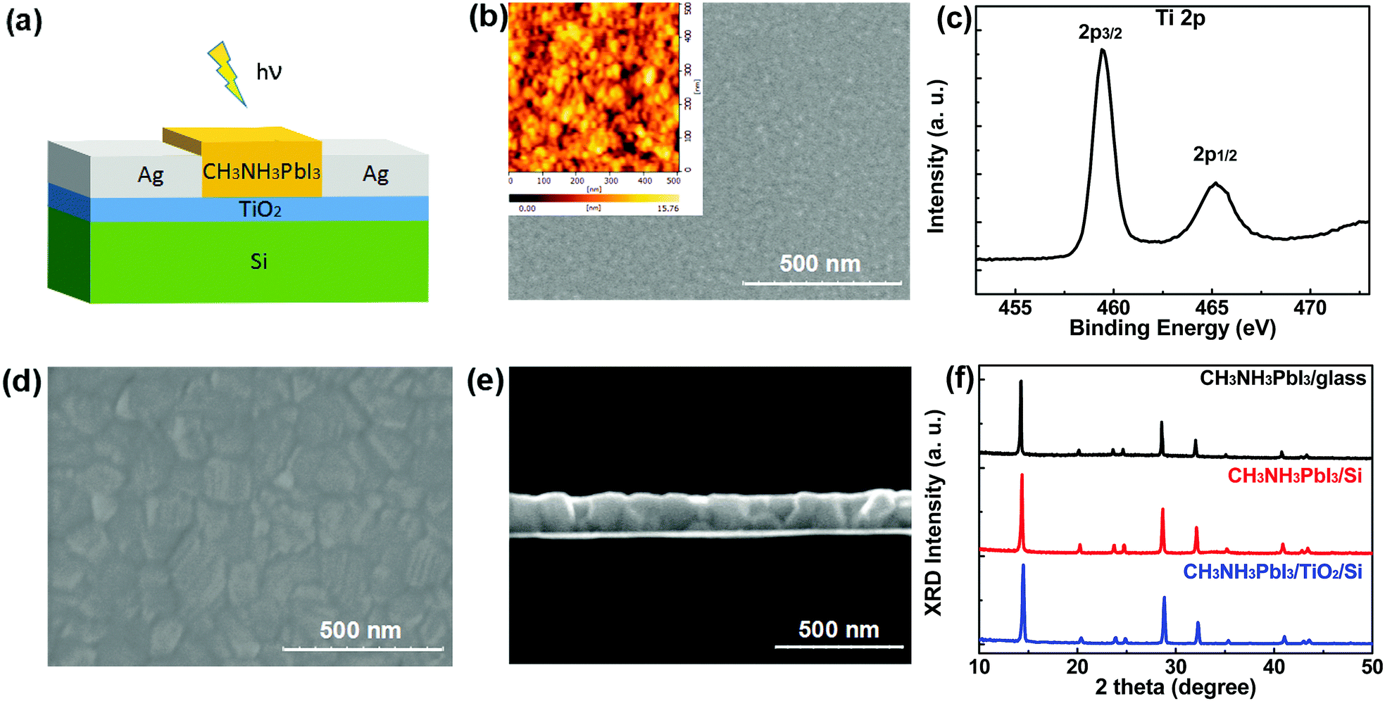 | ||
| Fig. 1 (a) Schematic structure of the CH3NH3PbI3/TiO2/Si PD. (b) Top-view SEM image and AFM image of the TiO2/Si film. (c) XPS of the TiO2/Si film. (d) Top-view SEM image of the CH3NH3PbI3/TiO2/Si film. (e) Cross-sectional SEM image of the CH3NH3PbI3/TiO2/Si film. (f) XRD spectra of the CH3NH3PbI3/glass, CH3NH3PbI3/Si and CH3NH3PbI3/TiO2/Si films. | ||
The surface morphology of the TiO2 film deposited on the Si substrate was acquired by top-view scanning electron microscopy (SEM) and atomic force microscopy (AFM), and the images are given in Fig. 1b (with the AFM image as an inset). Analysis of the images shows that the TiO2 film has a roughness of about 2.5 nm. A Ti 2p X-ray photoelectron spectroscopy spectrum of the TiO2 film is illustrated in Fig. 1c. The Ti1/2 and Ti3/2 spin-orbital splitting photoelectrons are located at 465.2 and 459.3 eV, respectively. The peak separation of 5.9 eV between the Ti 2P1/2 and 2P3/2 signals is consistent with those reported.34,35 The top-view SEM image of the CH3NH3PbI3/TiO2/Si film is shown in Fig. 1d. It is seen that the CH3NH3PbI3 film is almost pinhole-free, and consists of dense crystals with sizes in the 50–250 nm range. The cross-sectional SEM image given in Fig. 1e shows that the thickness of the perovskite film is about 180 nm. Huang reported that the nucleation and crystallization of the perovskite film heavily depend on the substrate.35 We compared the SEM images of the CH3NH3PbI3/glass, CH3NH3PbI3/Si and CH3NH3PbI3/TiO2/Si samples, as presented in Fig. S2 (ESI†). There is no obvious difference among the three samples. The X-ray diffraction (XRD) patterns of the three films are presented in Fig. 1f. The three typical peaks at 14.1°, 28.4°, and 31.9° can be assigned to the (110), (220), and (310) crystallographic planes of CH3NH3PbI3.8,14 It should be noted that no obvious signals from the TiO2 film can be observed due to its weak crystallization, which is in agreement with a previous report.36 A very strong Si(100) peak at 69.1° is observed and is not shown here. For the main (110) crystallographic planes of both the CH3NH3PbI3/Si and CH3NH3PbI3/TiO2/Si samples, the full width at half-maximum (FWHM) of the peak only increases slightly compared with that of the CH3NH3PbI3/glass sample. Therefore, these substrates in our experiment have negligible influence on the quality of the CH3NH3PbI3 film. As the improvement of the device parameters followed by the change in the order of magnitude (shown below), the slight differences in the perovskite film could not be the major reason for this.
We also performed photoluminescence (PL) measurements for the three samples. As shown in Fig. 2a, strong PL quenching is observed for both the CH3NH3PbI3/Si and CH3NH3PbI3/TiO2/Si samples (compared with the CH3NH3PbI3/glass sample). The time-resolved PL spectra for the three samples are given in Fig. 2b; it is seen that the CH3NH3PbI3/glass sample shows a PL lifetime of over 100 ns, which is about tenfold longer than those of the CH3NH3PbI3/Si and CH3NH3PbI3/TiO2/Si samples, which can be attributed to efficient interface-involved carrier transfer. As shown in Fig. 2c, the band alignments of both the CH3NH3PbI3/Si and CH3NH3PbI3/TiO2/Si samples enable them to form a heterojunction. For the CH3NH3PbI3/Si sample, photoholes generated in the CH3NH3PbI3 film can be injected into the Si, while photoelectrons are obstructed by the elevated interface barrier. For the CH3NH3PbI3/TiO2/Si sample, the TiO2 layer can efficiently facilitate (block) the photoelectron (photohole) transfer from the CH3NH3PbI3 into the Si. Thus the photoelectron and photoholes are largely spatially separated, and hence an enormous increase in photoresponse could be realized for both the CH3NH3PbI3/Si and CH3NH3PbI3/TiO2/Si PDs.
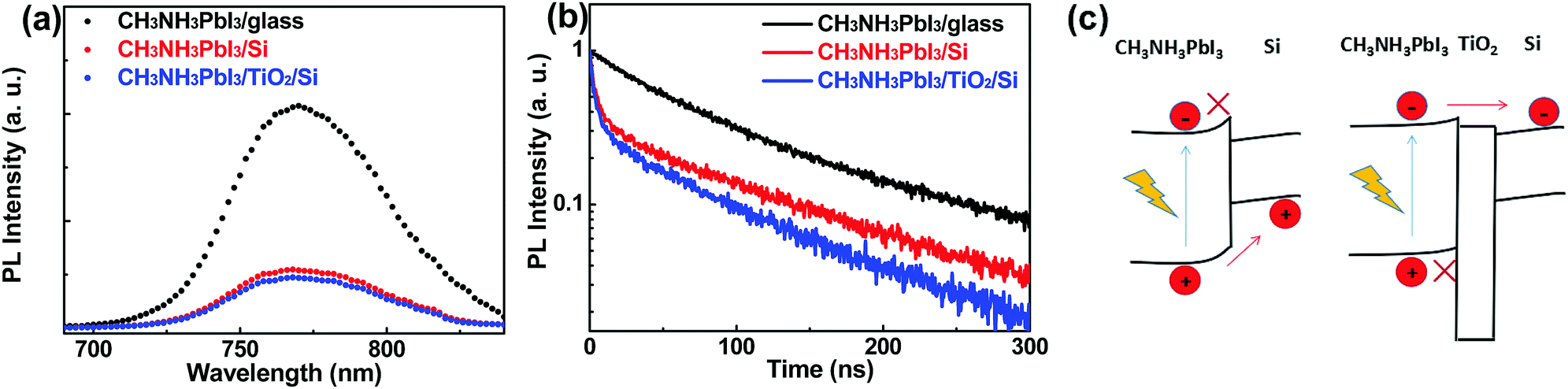 | ||
| Fig. 2 (a) Steady-state PL spectra. (b) Time-resolved PL spectra of the CH3NH3PbI3/glass, CH3NH3PbI3/Si and CH3NH3PbI3/TiO2/Si samples (under an excitation wavelength of 460 nm). (c) Band diagrams of the CH3NH3PbI3/Si and CH3NH3PbI3/TiO2/Si samples. | ||
The dark and light currents of PDs with different constructions (Si, CH3NH3PbI3/glass, CH3NH3PbI3/Si and CH3NH3PbI3/TiO2/Si) as a function of applied voltage are given in Fig. 3a and b, respectively. The PD parameters extracted under a bias of 10 V are summarized in Table 1. It is seen that the Si PD only presents a very low on/off ratio of 1.3. This can be explained as follows: Si possesses an intrinsically high conductance due to its high carrier mobility, and this leads to high dark current in the order of 10−5 A; meanwhile, Si is an indirect bandgap semiconductor and hence has weak light absorption, leading to low photocurrent (defined as the difference between light current and dark current). In comparison, the CH3NH3PbI3/glass PD has a much lower dark current in the order of 10−9 A, but still a relatively low on/off ratio of 116. The unsatisfactory light current is due to severe carrier recombination inside the CH3NH3PbI3 film, in which both electrons and holes are transported.6,8 By combining the CH3NH3PbI3 film with the Si substrate, the light current is enhanced significantly compared with the pure perovskite device. It should be attributed to the heterojunction formed at the CH3NH3PbI3/Si interface, which helps holes to flow into Si under illumination. This greatly suppresses the photogenerated carrier recombination and improves the photocurrent.36,37 However, although the dark current is lower than that for the Si device due to the depletion region, it is still in the order of 10−6 A, and such high dark current is detrimental to the light detecting capability of PDs. Encouragingly, by inserting a TiO2 layer, the CH3NH3PbI3/TiO2/Si PD exhibits a much lower dark current of 10−9 A as well as a comparable light current compared to that of the CH3NH3PbI3/Si PD. The high barrier for electron injection at the Ag/TiO2 interface effectively reduces the dark current from the Si substrate without any impact on the photocurrent in the CH3NH3PbI3 film.
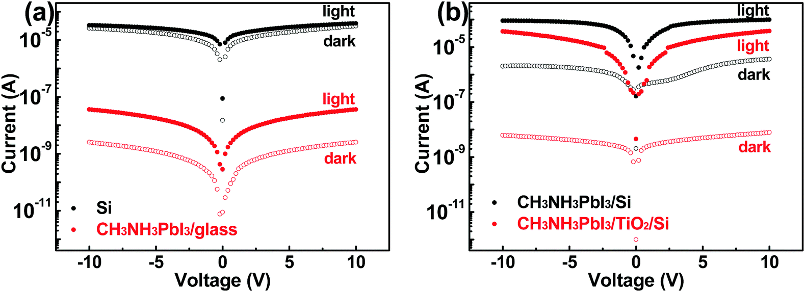 | ||
| Fig. 3 The dark current and light current (under 0.5 mW cm−2 white light illumination) as a function of applied voltage: (a) the Si and CH3NH3PbI3/glass PDs and (b) the CH3NH3PbI3/Si and CH3NH3PbI3/TiO2/Si PDs. | ||
| Structure | Dark current (A) | Light current (A) | On/off ratio | R (A W−1) | D* (Jones) |
|---|---|---|---|---|---|
| Si | 2.62 × 10⁻⁵ | 3.34 × 10⁻⁵ | 1.3 | 12.0 | 1.44 × 10¹¹ |
| CH3NH3PbI3/glass | 3.15 × 10⁻¹⁰ | 3.65 × 10⁻⁸ | 116 | 0.057 | 1.95 × 10¹¹ |
| CH3NH3PbI3/Si | 2.02 × 10⁻⁶ | 9.12 × 10⁻⁵ | 45 | 148.4 | 6.40 × 10¹² |
| CH3NH3PbI3/TiO2/Si | 6.23 × 10⁻⁹ | 3.75 × 10⁻⁵ | 6019 | 62.5 | 4.85 × 10¹³ |
Benefiting from the high photocurrent and low dark current, the CH3NH3PbI3/TiO2/Si PD exhibits a fairly high on/off ratio of 6.0 × 10³ and D* of 4.85 × 10¹³ Jones, with a decent R of 62.5 A W−1 (D* and R are two important parameters characterizing a PD device; their definitions and calculations are provided in the ESI†). Table S2 (ESI†) lists the device parameters of current typical perovskite-based PDs. It is seen that the PDs with high R (usually use highly conductive graphene or its derivatives) have very low on/off ratios, and the ones with high on/off ratios have very low R. In comparison, the CH3NH3PbI3/TiO2/Si PD we designed here shows high overall performance. In addition, a device simulation was made to verify our analysis, which is presented in the ESI,† Fig. S5. In order to confirm the reliability and reproducibility of our results, the experiments were conducted repeatedly. The histograms of dark and light currents at a bias of 10 V for the CH3NH3PbI3/TiO2/Si PD were collected from 20 independent products.
Fig. 4a shows the photocurrent and R dependences on light power for the CH3NH3PbI3/TiO2/Si PD. It is seen that the photocurrent increases, while R decreases with increasing light illumination. The decrease of R is a trap state induced effect.38Fig. 4b shows the spectral response of the CH3NH3PbI3/TiO2/Si PD. It is seen that, benefiting from the light absorption of narrow-bandgap Si, the photoresponse wavelength reaches 1100 nm. In comparison, the response of the CH3NH3PbI3/glass PD is cut off at 780 nm.20 The on–off switching properties of the CH3NH3PbI3/TiO2/Si PD are presented in Fig. 4c and d. It is seen that the PD can be switched on and off repeatedly and stably, and the rise time and decay time are 0.89 s and 0.42 s, respectively (the rise time is defined as the time for the current to increase to 90% of the peak value and the decay time is defined as the time for the current to decay to 10% of the peak value38–40).
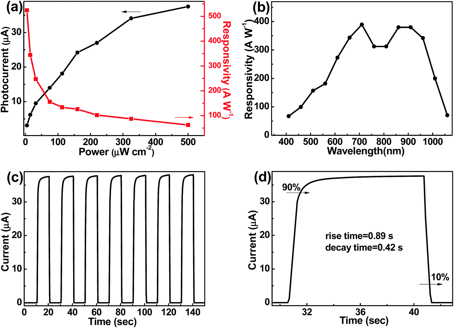 | ||
| Fig. 4 (a) Photocurrent and responsivity of the CH3NH3PbI3/TiO2/Si PD versus white light illumination power at a bias of 10 V. (b) Responsivity of the CH3NH3PbI3/TiO2/Si PD under 10.6 μW cm−2 illumination with various wavelengths at a bias of 10 V. (c and d) On–off switching properties of the CH3NH3PbI3/TiO2/Si PD at a bias of 10 V. | ||
Conclusions
In summary, CH3NH3PbI3-Si hybrid PDs are fabricated and investigated. The reduced recombination due to the spatial separation of photocarriers significantly enhances the photocurrent. Further, by inserting a thin TiO2 layer in-between the CH3NH3PbI3 film and the Si substrate, the dark current is greatly suppressed. The designed CH3NH3PbI3/TiO2/Si PD shows excellent overall performance with a high on/off ratio of 6 × 10³ and a high D* of 4.85 × 10¹³ Jones. Moreover, the PD shows broad photoresponse reaching 1100 nm, which is helped by light absorption from the Si. Our work here provides a feasible strategy for developing high-performance perovskite-based PDs.Experimental
Material synthesis and device fabrication
A TiO2 solution was made using previously reported sol–gel methods:2,40 1 mL TiCl4 (99.9%, Alfa) was added into 4 mL anhydrous ethanol. The mixed solution was then stirred, then 20 mL benzyl alcohol was added. The obtained solution is yellow in color and was stored at 85 °C for one whole night. The solution was then mixed with 400 mL diethyl ether and centrifuged at 6000 rpm for 2 min to obtain TiO2 nanocrystal precipitates. Finally, the TiO2 nanocrystals were dispersed into anhydrous chloroform and anhydrous methanol (1![[thin space (1/6-em)]](https://www.rsc.org/images/entities/char_2009.gif) :1 volume ratio) with a concentration of about 5 mg mL−1. A perovskite precursor (0.5 M) was prepared by dissolving CH3NH3I and PbI2 in a 1:1 molar ratio in a 4:1 (v:v) mixed solvent of N,N-dimethylformamide (DMF) and dimethylsulfoxide (DMSO). The solution was then heated at 60 °C for 12 hours for sufficient dissolution. A Si substrate (2–5 Ω cm) was sequentially cleaned using detergent, acetone, and isopropanol with ultrasonication for 10 min each and then was immersed into 10% HF solution for 1 min to remove the native oxide layer. After that, the Si substrate was dried and treated with O2 plasma for 5 min. The TiO2 solution was spin-coated on the substrate at 6000 rpm for 30 s, and annealed in ambient air at 150 °C for 30 min. After that, 80 nm-thick Ag electrodes were thermally deposited on the TiO2 film through a shadow mask, resulting in a channel length of 60 μm and a channel width of 2000 μm. The perovskite film was then fabricated on top using an anti-solvent spin coating procedure.
:1 volume ratio) with a concentration of about 5 mg mL−1. A perovskite precursor (0.5 M) was prepared by dissolving CH3NH3I and PbI2 in a 1:1 molar ratio in a 4:1 (v:v) mixed solvent of N,N-dimethylformamide (DMF) and dimethylsulfoxide (DMSO). The solution was then heated at 60 °C for 12 hours for sufficient dissolution. A Si substrate (2–5 Ω cm) was sequentially cleaned using detergent, acetone, and isopropanol with ultrasonication for 10 min each and then was immersed into 10% HF solution for 1 min to remove the native oxide layer. After that, the Si substrate was dried and treated with O2 plasma for 5 min. The TiO2 solution was spin-coated on the substrate at 6000 rpm for 30 s, and annealed in ambient air at 150 °C for 30 min. After that, 80 nm-thick Ag electrodes were thermally deposited on the TiO2 film through a shadow mask, resulting in a channel length of 60 μm and a channel width of 2000 μm. The perovskite film was then fabricated on top using an anti-solvent spin coating procedure.
Characterization
Electrical characterization data were recorded with a Keithley 4200 in ambient air. Monochromatic light and white light were from a Newport Oriel 200 and a XZ-150WA halogen lamp, respectively. Prior to the utilization of the light, the spectral and light intensity were calibrated using a monosilicon detector. In detail, the I–V curves were measured in reverse (10 V to −10 V) or forward (−10 V to 10 V) mode. The step voltage and decay time were fixed at 200 mV and 10 ms, respectively. The optical images were obtained using an Olympus BX51 optical microscope. The morphology of the formed film and the cross-sectional image were characterized by SEM (Hitachi S-4800). An AFM image was obtained using a Dimension Icon microscope. Visible spectra were recorded using a JASCO V-570 spectrophotometer and PL spectra were characterized using a JASCO FP-6600 spectrophotometer with a Xenon flash lamp. XPS spectra were obtained using a KRATOS ULTRA AXIS DLD photoelectron spectroscopy system with an Al X-ray source. XRD patterns were obtained using a Rigaku D/MAX-2004 XRD with Cu Kα radiation (λ = 1.54178 Å).Author contributions
The most experiments (including simulation) and data analysis were performed by Xiaohui Yi. The AFM was performed with the help of Yisen Wang. Zhengwei Ren helped in synthesising the TiO2 NCs. The XPS and PL were performed with the help of Yisen Wang. Zhiwei Huang and Hui Li participated in discussion and provided some useful advice. The manuscript was written by Xiaohui Yi, Tao Lin, Cheng Li and Jizheng Wang. All authors reviewed the manuscript.Conflicts of interest
There are no conflicts to declare.Acknowledgements
This research was supported by the National Natural Science Foundation of China (61474094 and 61405208), the National Key Research Program of China (2016YFA0200104), the 973 Program (2014CB643600 and 2014CB643503), and the Strategic Priority Research Program of the Chinese Academy of Sciences (XDB12030200).Notes and references
- H. Zhou, Q. Chen, G. Li, S. Luo, T. Song, H. Duan, Z. Hong, J. You, Y. Liu and Y. Yang, Science, 2014, 345, 6196 Search PubMed.
- W. Nie, H. Tsai, R. Asadpour, J.-C. Blancon, A. J. Neukirch, G. Gupta, J. J. Crochet, M. Chhowalla, S. Tretiak, M. A. Alam, H.-L. Wang and A. D. Mohite, Science, 2015, 347, 6221 CrossRef PubMed.
- D.-Y. Son, J.-W. Lee, Y. J. Choi, I.-H. Jang, S. Lee, P. J. Yoo, H. Shin, N. Ahn, M. Choi, D. Kim and N.-G. Park, Nat. Energy, 2016, 1, 16081 CrossRef.
- Z. Zhu, Y. Bai, X. Liu, C.-C. Chueh, S. Yang and Al. K.-Y. Jen, Adv. Mater., 2016, 28, 6478 CrossRef PubMed.
- W. S. Yang, B.-W. Park, E. H. Jung, N. J. Jeon, Y. C. Kim, D. U. Lee, S. S. Shin, J. Seo, E. K. Kim, J. H. Noh and S. I. Seok, Science, 2017, 356, 1376 CrossRef PubMed.
- Y. Zhang, J. Du, X. Wu, G. Zhang, Y. Chu, D. Liu, Y. Zhao, Z. Liang and J. Huang, ACS Appl. Mater. Interfaces, 2015, 7, 21634 CrossRef PubMed.
- X. Hu, X. Zhang, L. Liang, J. Bao, S. Li, W. Yang and Y. Xie, Adv. Mater., 2014, 24, 7373 Search PubMed.
- H. Lu, W. Tian, F. Cao, Y. Ma, B. Gu and L. Li, Adv. Func. Mater., 2016, 26, 1296 CrossRef.
- K. C. Kwon, K. Hong, Q. V. Le, S. Y. Lee, J. Choi, K.-B. Kim, S. Y. Kim and H. W. Jang, Adv. Funct. Mater., 2016, 26, 4213 CrossRef.
- Y. Lee, J. Kwon, E. Hwang, C.-H. Ra, W. J. Yoo, J.-H. Ahn, J. H. Park and J. H. Cho, Adv. Mater., 2015, 27, 41 CrossRef PubMed.
- Y. Wang, Y. Zhang, Y. Lu, W. Xu, H. Mu, C. Chen and H. Qiao, Adv. Opt. Mater., 2015, 3, 1389 CrossRef.
- Z. Sun, L. Aigouy and Z. Chen, Nanoscale, 2016, 8, 7377 RSC.
- M. Spina, M. Lehmann, B. Náfrádi, L. Bernard, E. Bonvin, R. Gaál, A. Magrez, L. Forró and E. Horváth, Small, 2015, 11, 4824 CrossRef PubMed.
- C. Ma, Y. Shi, W. Hu, M.-H. Chiu, Z. Liu, A. Bera, F. Li, H. Wang, L.-J. Li and T. Wu, Adv. Mater., 2016, 28, 3683 CrossRef PubMed.
- D.-H. Kang, S. R. Pae, J. Shim, G. Yoo, J. Jeon, J. W. Leem, J. S. Yu, S. Lee, B. Shin and J.-H. Park, Adv. Mater., 2016, 28, 7799 CrossRef PubMed.
- Y. Wang, R. Fullon, M. Acerce, C. E. Petoukhoff, J. Yang, C. Chen, S. Du, S. Ki Lai, S. P. Lau, D. Voiry, D. O’Carroll, G. Gupta, A. D. Mohite, S. Zhang, H. Zhou and M. Chhowalla, Adv. Mater., 2017, 29, 1603995 CrossRef PubMed.
- J. Lu, A. Carvalho, H. Liu, S. X. Lim, A. H. C. Neto and C. H. Sow, Angew. Chem., 2016, 128, 12124 CrossRef.
- L. Zhou, K. Yu, F. Yang, J. Zheng, Y. Zuo, C. Li, B. Cheng and Q. Wang, Dalton Trans., 2017, 46, 1766 RSC.
- J. Yu, X. Chen, Y. Wang, H. Zhou, M. Xue, Y. Xu, Z. Li, C. Ye, J. Zhang, P. A. van Aken, P. D. Lundac and H. Wang, J. Mater. Chem. C, 2016, 4, 7302 RSC.
- X. Yi, Z. Ren, N. Chen, C. Li, X. Zhong, S. Yang and J. Wang, Adv. Electron. Mater., 2017, 1700251 CrossRef.
- S. Chen, C. Teng, M. Zhang, Y. Li, D. Xie and G. Shi, Adv. Mater., 2016, 28, 5969 CrossRef PubMed.
- Y. Guo, C. Liu, H. Tanaka and E. Nakamura, J. Phys. Chem. Lett., 2015, 6, 535 CrossRef PubMed.
- S. Tong, J. Sun, C. Wang, Y. Huang, C. Zhang, J. Shen, H. Xie, D. Niu, S. Xiao, Y. Yuan, J. He, J. Yang and Y. Gao, Adv. Electron. Mater., 2017, 1700058 CrossRef.
- H. Wang and D. H. Kim, Chem. Soc. Rec., 2017, 46, 5204 RSC.
- L. Li, Y. Deng, C. Bao, Y. Fang, H. Wei, S. Tang, F. Zhang and J. Huang, Adv. Opt. Mater., 2017, 5, 1700672 CrossRef.
- W. Wang, D. Zhao, F. Zhang, L. Li, M. Du, C. Wang, Y. Yu, Q. Huang, M. Zhang, L. Li, J. Miao, Z. Lou, G. Shen, Y. Fang and Y. Yan, Adv. Funct. Mater., 2017, 27, 1703953 CrossRef.
- W. Wang, F. Zhang, M. Du, L. Li, M. Zhang, K. Wang, Y. Wang, B. Hu, Y. Fang and J. Huang, Nano Lett., 2017, 17, 1995 CrossRef PubMed.
- L. Qian, Y. Sun, M. Wu, D. Xie, L. Ding and G. Shi, Adv. Mater., 2017, 29, 1606175 CrossRef PubMed.
- S. Ke, S. Lin, X. Li, J. Li, J. Xu, C. Li and S. Chen, Opt. Express, 2016, 24, 1943 CrossRef PubMed.
- G. Lin, X. Yi, C. Li, N. Chen, L. Zhang, S. Chen, W. Huang, J. Wang, X. Xiong and J. Sun, Appl. Phys. Lett., 2016, 109, 141104 CrossRef.
- X. Li, J. E. Carey, J. W. Sickler, M. U. Pralle, C. Palsule and C. J. Vineis, Opt. Express, 2012, 20, 5518 CrossRef PubMed.
- L.-D. Haret, X. Checoury, Z. Han, P. Boucaud, S. Combrié and A. D. Rossi, Opt. Express, 2010, 18, 23965 CrossRef PubMed.
- K.-F. Lin, S. H. Chang, K.-H. Wang, H.-M. Cheng, K. Y. Chiu, K.-M. Lee, S.-H. Chen and C.-G. Wu, Sol. Energy Mater. Sol. Cells, 2015, 141, 309 CrossRef.
- Z. Song, J. Hrbek and R. Osgood, Nano Lett., 2005, 5, 1327 CrossRef PubMed.
- B. Erdem, R. A. Hunsicker, G. W. Simmons, E. D. Sudol, V. L. Dimonie and M. S. El-Aasser, Langmuir, 2001, 17, 2664 CrossRef.
- (a) H. Tan, A. Jain, O. Voznyy, X. Lan, F. P. G. de Arquer, J. Z. Fan, R. Q. Bermudez, M. Yuan, B. Zhang, Y. Zhao, F. Fan, P. Li, L. N. Quan, Y. Zhao, Z.-H. Lu, Z. Yang, S. Hoogland and E. H. Sargent, Science, 2017, 355, 722 CrossRef PubMed; (b) J. Zhao, Y. Deng, H. Wei, X. Zheng, Z. Yu, Y. Shao, J. E. Shield and J. Huang, Sci. Adv., 2017, 3, 5616 CrossRef PubMed.
- Z. Jin and J. Wang, J. Mater. Chem. C, 2013, 1, 7996 RSC.
- Z. Qi, J. Cao, H. Li, L. Ding and J. Wang, Adv. Funct. Mater., 2015, 25, 3138 CrossRef.
- Z. Jin, Q. Zhou, Y. Chen, P. Mao, H. Li, H. Liu, J. Wang and Y. Li, Adv. Mater., 2016, 28, 3697 CrossRef PubMed.
- J. Zhang, Q. Wang, L. Wang, X. Li and W. Huang, Nanoscale, 2015, 7, 10391 RSC.
Footnote |
| † Electronic supplementary information (ESI) available: Optical microscopy image, schematic structures, SEM images, I–V curve, on–off switching properties, and device simulation. See DOI: 10.1039/c8qm00303c |
| This journal is © the Partner Organisations 2018 |