
 Open Access Article
 This Open Access Article is licensed under a
 Creative Commons Attribution 3.0 Unported Licence
Cs1−xRbxSnI3 light harvesting semiconductors for perovskite photovoltaics†
Kenneth P.
Marshall
a,
Shuxia
Tao
 b,
Marc
Walker
c,
Daniel S.
Cook
a,
James
Lloyd-Hughes
c,
Silvia
Varagnolo
a,
Anjana
Wijesekara
a,
David
Walker
c,
Richard I.
Walton
a and
Ross A.
Hatton
*a
b,
Marc
Walker
c,
Daniel S.
Cook
a,
James
Lloyd-Hughes
c,
Silvia
Varagnolo
a,
Anjana
Wijesekara
a,
David
Walker
c,
Richard I.
Walton
a and
Ross A.
Hatton
*a
aDepartment of Chemistry, University of Warwick, CV4 7AL, Coventry, UK. E-mail: Ross.Hatton@warwick.ac.uk
bCenter for Computational Energy Research, Department of Applied Physics, Technische Universiteit Eindhoven, P.O. Box 513 5600 MB, Eindhoven, The Netherlands
cDepartment of Physics, University of Warwick, CV4 7AL, Coventry, UK
First published on 13th June 2018
Abstract
We show that films of the 3-dimensional perovskite Cs1−xRbxSnI3 can be prepared from room temperature N,N-dimethylformamide solutions of RbI, CsI and SnCl2 for x ≤ 0.5, and that for x ≤ 0.2 film stability is sufficient for utility as the light harvesting layer in inverted photovoltaic (PV) devices. Electronic absorption and photoluminescence spectroscopy measurements supported by computational simulation, show that increasing x increases the band gap, due to distortion of the lattice of SnI6 octahedra that occurs when Cs is substituted with Rb, although it also reduces the stability towards decomposition. When Cs0.8Rb0.2SnI3 perovskite is incorporated into the model inverted PV device structure; ITO|perovskite|C60|bathocuproine|Al, an ∼120 mV increase in open-circuit is achieved which is shown to correlate with an increase in perovskite ionisation potential. However, for this low Rb loading the increase in band gap is very small (∼30 meV) and so a significant increase in open circuit-voltage is achieved without reducing the range of wavelengths over which the perovskite can harvest light. The experimental findings presented are shown to agree well with the predictions of density functional theory (DFT) simulations of the stability and electronic structure, also performed as part of this study.
Introduction
The black gamma (B-γ) polymorph of CsSnI3 perovskite is a promising material for photovoltaic (PV) applications because it offers an ideal band gap for single junction PV devices (∼1.34 eV1) together with a high electron and hole mobility (1.6 and 585 cm2 V−1 s−1, respectively)1,2 and small exciton binding energy.3,4 This wholly inorganic perovskite comprises a 3-dimensional structure of corner sharing SnI6 octahedra with Cs cations surrounded by 8 SnI6 octahedra, and adopts the orthorhombic B-γ phase below 89 °C.2 To date it has been used as the light harvesting semiconductor in PV devices based on mesoporous TiO25,6 and planar7–9 device architectures, demonstrating the potential to achieve very high short circuit current density (Jsc) of >20 mA cm−2 under one sun illumination6 and high device fill factor (FF).8 The primary factor limiting the power conversion efficiency of B-γ CsSnI3 based PVs is the low open-circuit voltage (Voc): to date the highest Voc reported is 0.55 V,8 achieved for an inverted device architecture using phenyl-C61-butyric acid methylester (PCBM) as the electron transport layer (ETL), which is approximately half that attainable using the lead analogue CsPbI3.10 When using C60 in place of PCBM the highest Voc reported is reduced to 0.36 V due to the larger electron affinity of the former.9The Voc in inverted perovskite PV devices depends strongly on a number of factors including the energetics at the perovskite-ETL interface7 and the degree of crystallinity in the ETL.11 Additionally, for PV devices using B-γ CsSnI3 as the light harvesting layer, we have shown that SnCl2 is an effective additive for reducing the density of tin vacancy defects in the band gap and reducing the reverse saturation current,8 both of which help to improve Voc. However, Voc is ultimately limited by the relatively small ionisation potential (Ip) of B-γ CsSnI3 of ∼4.9 eV,9,12 which is approximately half an electron volt smaller than that of lead halide perovskites.13 Fortunately, similar to lead halide perovskites, B-γ CsSnI3 is amenable to substitution of iodide ions with bromide ions, which results in an increase in Ip and band gap which translates to an increase in Voc in PV devices.14 However, this benefit must be balanced against the inevitable reduction in short circuit current density (Jsc) resulting from fewer photons having sufficient energy to excite electrons across the larger band gap. An alternative strategy for tuning the electronic structure of B-γ CsSnI3 is substitution of A-site Cs cation with the smaller Rb cation to form Cs1−xRbxSnI3. Unlike the case of halide ion substitution, the orbitals of the A-site metal cation do not contribute directly to the conduction and valance band edges,4,15 but still indirectly affect the band gap as a result of the distortion of the lattice of SnI6 octahedra via tilting that occurs when reducing the size of the A-site ion.16,17 RbSnI3 has a tolerance factor of 0.840 which is very close to the value that allows for the likely formation of a 3D structure; 0.85,18 which is consistent with the fact that it has only been reported in the one-dimensional yellow phase.19
Herein we report the facile room temperature preparation of thin films of 3-dimensional (3D) Cs1−xRbxSnI3 and show how partial exchange of Cs with Rb can be used to increase Ip and band gap. Notably, for low levels of substitution it is possible to achieve a significant increase in Ip with only a very small increase in band gap which, in model inverted PV devices, results in a sizable increase in Voc with no significant adverse impact on the light harvesting capability. The experimental findings presented are shown to agree well with the predications of density functional theory (DFT) simulations of the stability and electronic structure, also performed as part of this study.
Results and discussion
The tin halides SnI2, SnCl2 and SnF2 are typically used as a source of excess Sn during the preparation of B-γ CsSnI3 films to minimise the density of tin vacancy defects.5,7,8,12 In the first part of this study SnI2 was used as the source of excess Sn to avoid the possibility that Cl or F might be incorporated into the lattice of Cs1−xRbxSnI3, which would complicate the interpretation. Films of Cs1−xRbxSnI3 were prepared with Rb content x = 0, 0.2, 0.5, 0.8 and 1, with a thickness of ∼50 nm on ITO glass and ∼80 nm on plain glass. All films were deposited under nitrogen by spin casting from solutions of N,N-dimethylformamide (DMF) at room temperature. Films prepared with x = 0, 0.2 and 0.5 (Fig. S1, ESI†) were an intense dark colour typical of 3D tin halide perovskite, whilst films with x = 0.8 and 1 were orange/yellow in colour indicating that they did not form 3D perovskite phases.Fig. 1 shows the X-ray diffraction (XRD) patterns for ∼80 nm thick Cs1−xRbxSnI3 films supported on glass at room temperature, along with simulated patterns for B-γ CsSnI3 and RbSnI3. It is evident from these patterns that for x = 0 and 0.2 the crystal structure is similar to that of B-γ CsSnI3. For x = 0.5 the films were very unstable, with the colour evolving from a deep red to yellow in the few minutes taken to load the sample into the X-ray diffractometer.
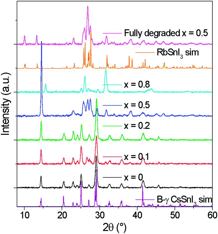 | ||
| Fig. 1 XRD patterns of Cs1−xRbxSnI3 where x = 0, 0.1, 0.2, 0.5, 0.8 with simulated patterns of B-γ CsSnI3. All films were deposited from DMF solutions of RbI, CsI and SnI2 at room temperature. | ||
Lattice parameter fitting; ESI† (Fig. S2), shows there is no significant or systematic change in lattice parameters between B-γ CsSnI3, Cs0.9Rb0.1SnI3 and Cs0.8Rb0.2SnI3, entirely consistent with the computational simulations of Jung et al.16 and DFT simulations performed as part of this study (ESI,† Fig. S3 and S4), both of which predict only a small change in lattice parameters between the 3D perovskite B-γ CsSnI3 and the hypothetical 3D RbSnI3, due to a much higher degree of tilting between the corner sharing SnI6 octahedra in the latter. Simulation of the X-ray diffraction pattern based on a crystallographic information file of CsSnI3 in which 20% of Cs atoms have been replaced with Rb atoms shows that there should be some difference in the peak intensities (Fig. 2): the simulation predicts that the (101) and (020) reflections should have increased intensity relative to the (202) and (040) reflections when Cs is partially substituted with Rb. Comparing the measured patterns of Cs1−xRbxSnI3 there is no significant trend in the relative ratios of the (101) + (020)![[thin space (1/6-em)]](https://www.rsc.org/images/entities/char_2009.gif) :(202) + (040) intensities, although both samples incorporating Rb have higher relative intensities of (101) and (020) compared with (202). Additionally, before the sample degraded the Cs0.5Rb0.5SnI3 sample has a very intense peak at 14.5° which is assigned to (101) and (020) Miller planes for perovskite material. By comparison, the fully degraded Cs0.5Rb0.5SnI3 has peaks at 10.0° and 13.3°, characteristic of the yellow phase.2,19 It should be noted that preferred orientation effects may also modify the relative intensities of reflections, indeed we have previously shown that B-γ CsSnI3 films deposited in the same way as used in the current study can exhibit substrate specific preferred crystallite orientation.9 Since the degree of orientation may also conceivably be affected by the compositions of the samples this analysis cannot be quantified.
:(202) + (040) intensities, although both samples incorporating Rb have higher relative intensities of (101) and (020) compared with (202). Additionally, before the sample degraded the Cs0.5Rb0.5SnI3 sample has a very intense peak at 14.5° which is assigned to (101) and (020) Miller planes for perovskite material. By comparison, the fully degraded Cs0.5Rb0.5SnI3 has peaks at 10.0° and 13.3°, characteristic of the yellow phase.2,19 It should be noted that preferred orientation effects may also modify the relative intensities of reflections, indeed we have previously shown that B-γ CsSnI3 films deposited in the same way as used in the current study can exhibit substrate specific preferred crystallite orientation.9 Since the degree of orientation may also conceivably be affected by the compositions of the samples this analysis cannot be quantified.
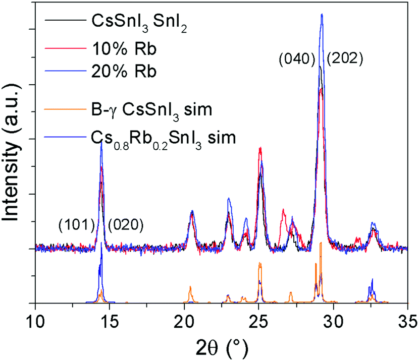 | ||
| Fig. 2 XRD patterns of Cs1−xRbxSnI3 where x = 0, 0.1, or 0.2, with simulated patterns of B-γ CsSnI32 and of CsSnI3 in which 20% of Cs atoms are replaced by Rb. | ||
To determine how the stability of the 3D perovskite films in ambient air depends on Rb content, the evolution of the absorption spectrum of Cs1−xRbxSnI3 films with a thickness of ∼50 nm on glass substrates was monitored as a function of time in ambient air. It is evident from Fig. 3 that incorporation of Rb into the lattice destabilises the film towards oxidation in air since there is a faster degradation of the absorption spectra with time with increasing Rb content, although for low Rb content (10%) this effect is relatively small. The observed reduction in stability with increasing substitution of Cs with Rb is consistent with the results of DFT calculation (Fig. 4), which show that the formation energy of the yellow phase of Cs1−xRbxSnI3 from the 3D perovskite is slightly exothermic and becomes increasingly exothermic with increasing Rb content, facilitating the formation of the yellow phase. DFT simulations also show that the yellow phase of Cs1−xRbxSnI3 will spontaneously convert to (Cs1−xRbx)2SnI6 upon exposure to O2 in air due to the large negative formation energies of the oxidised products. The reduction in stability with increasing Rb content is attributed to the increased octahedral tilting that results from substitution of Cs by Rb, leading to increased strain. Direct evidence for increased octahedral tilting of the lattice upon incorporation of Rb, based on measurement of the optical band gap and DFT simulation, is discussed below. Corroborating evidence for a distortion of the Sn–I–Sn bonds with increasing Rb content is also provided by core level photoelectron spectroscopy; ESI,† Fig. S5(a), which shows a continuous increase in the binding energy of the Sn3d peaks with increasing Rb substitution. Notably, scanning electron microscopy images of films with x = 0 and x = 0.2 and x = 0.5 (ESI,† Fig. S7) show that the film porosity significantly increases with increasing Rb content, which may also partially account for the differences in film stability, since more porous films have an increased surface area to volume ratio.
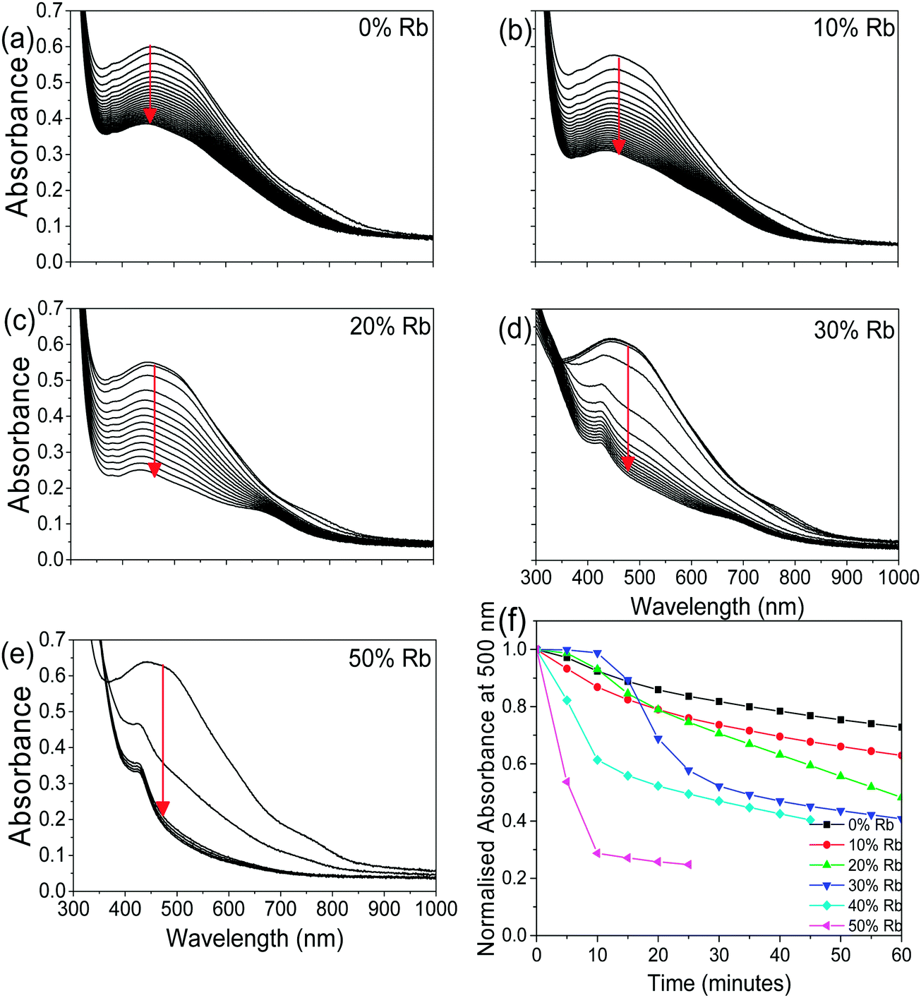 | ||
| Fig. 3 (a–e) UV/vis/NIR spectra as a function of time in air (measurements made every 5 minutes) for Cs1−xRbxSnI3:SnI2 with x = 0, 0.1, 0.2, 0.3, and 0.5. (f) Evolution of normalised absorbance at a wavelength of 500 nm for data shown in (a–e) as a function of time in ambient air. Data for x = 40 are given in ESI,† Fig. S6. | ||
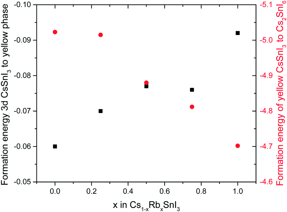 | ||
| Fig. 4 Calculated formation energy of yellow Cs1−xRbxSnI3 from 3D Cs1−xRbxSnI3 perovskites (black squares) and formation energy of Cs1−xRbxSnI6 from yellow Cs1−xRbxSnI3 (red circles). Both energy scales are in electron volts (eV). | ||
Fig. 5 shows the photoluminescence spectra for encapsulated Cs1−xRbxSnI3 films with increasing Rb content, from which it is evident that the band gap increases with increasing x from ∼1.34 eV to ∼1.50 eV. Films with x = 0.5 were found to be unstable even with encapsulation under nitrogen and so the spectrum shown in Fig. 5 is a sample before complete degradation. The increase in band gap with increasing Rb substitution is consistent with the electronic structure calculations performed as part of this study using the DFT-1/2 method: Fig. 6. The DFT-1/2 method has the advantage of improved accuracy in band gap calculation by introducing a half-electron/half-hole occupation, and has been successfully applied for the accurate prediction of band gaps of several metal halide perovskites including CsSnI3.20 The smaller size of Rb compared with Cs increases tilting of the SnI6 octahedra, which reduces Sn–I orbital overlap leading to a larger band gap.16,17 The increase in band gap is also compelling evidence that phase separation between domains of RbSnI3 and B-γ CsSnI3 does not occur, since RbSnI3 is predicted to have a much larger band gap than B-γ CsSnI3 (Fig. 6 and ref. 16) and so the photoluminescence spectrum of a film with phase separated domains of RbSnI3 and B-γ CsSnI3 would still have a significant peak at 1.34 eV. It is evident from Fig. 6 that for x = 0.2 the measured band gap is significantly smaller than predicted. This disparity is attributed to the relatively small structural model used in the DFT calculations which will overestimate the distortion of the lattice and the octahedral tilting for small x; ESI,† Fig. S3 and S4, giving rise to an overestimate of the band gap. However, the simulation correctly predicts the trend of increasing band gap with increasing Rb content, and for larger x the simulation and experiment are quantitatively in close agreement.
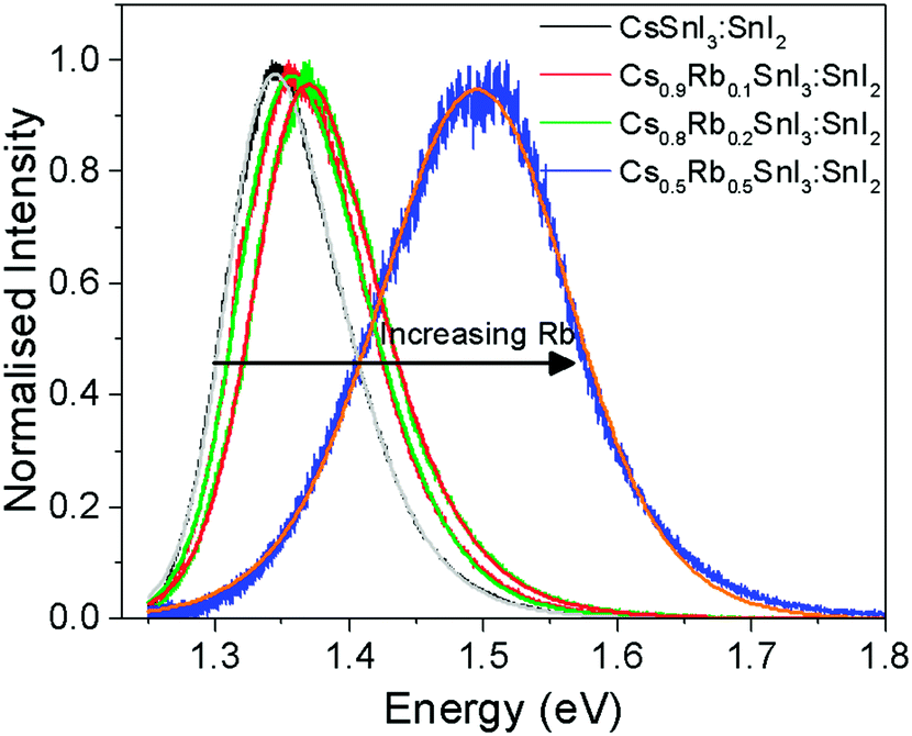 | ||
| Fig. 5 Photoluminescence spectra of Cs1−xRbxSnI3, where x = 0, 0.1, 0.2, and 0.5, including fits for each data set, with maxima at 1.34 ± 0.06 eV, 1.36 ± 0.08 eV, 1.37 ± 0.05 eV and 1.5 ± 0.11 eV, respectively. Errors given are full peak width at half maximum. | ||
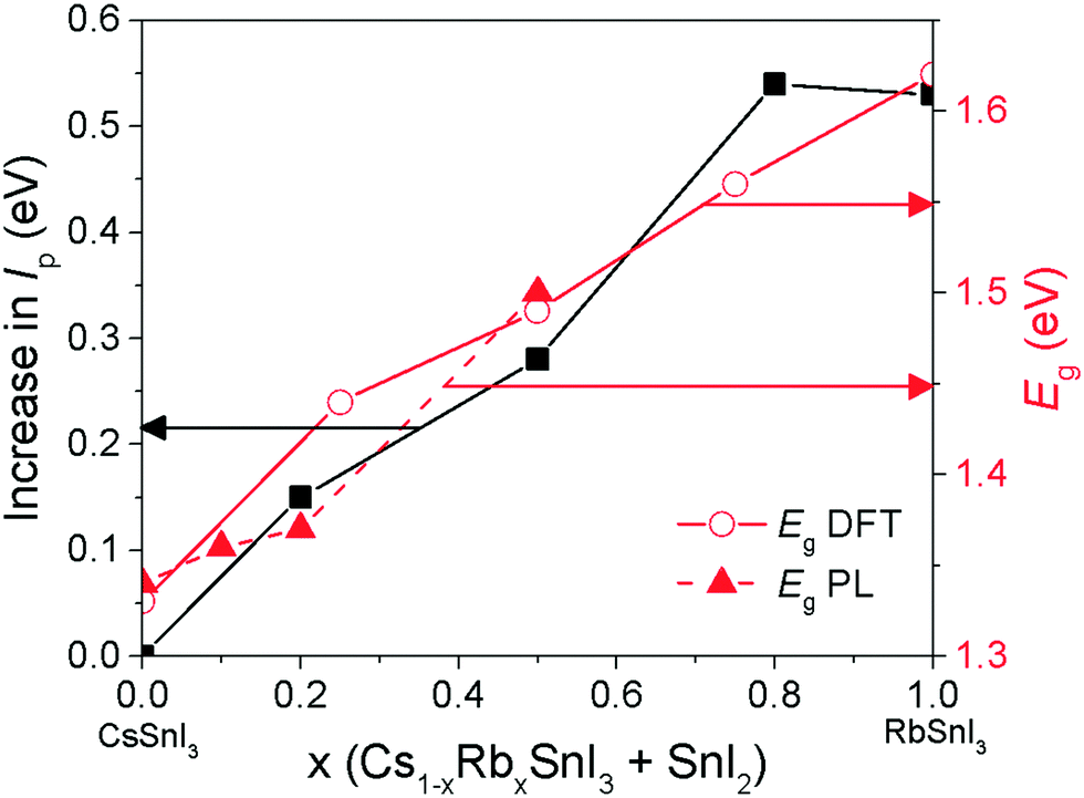 | ||
| Fig. 6 Evolution of band gap (Eg) and increase in Ip for Cs1−xRbxSnI3 with increasing Rb substitution (x). Band gap measured using photoluminescence spectroscopy (filled red triangles) and predicted using DFT-1/2 (open red circles). Increase in Ip measured using UPS (filled black squares). The connecting lines are included to guide the eye. The uncertainty in the DFT calculations is approximately ±0.1 eV. | ||
Further evidence of the uniform inclusion of Rb into the perovskite lattice is provided by the Cs:Rb elemental ratio estimated from the XPS peak intensities: ESI,† Table S1. The Cs:Rb ratios for those compositions that result in a stable perovskite structure (i.e. Rb ≤ 50% substitution) are in close agreement with the ratio used in the preparative solution. Since 95% of the XPS signal originates from the top ∼8 nm of the perovskite film,8 this can only be the case if the Rb is uniformly incorporated into the perovskite lattice. Taken together with the photoluminescence spectroscopy, valence band photoelectron spectroscopy and prediction of simulation, this provides compelling evidence for the inclusion of Rb in to the perovskite lattice.
The potential of these materials as the light harvester in PV devices was tested in the model inverted device architecture: ITO|Cs1−xRbxSnI3:10 mol% SnI2|C60|BCP|Al, for x = 0, 0.2, or 0.5. Whilst using C60 as the ETL is known to give a lower Voc than can be achieved using PCBM, due to its lower lying lowest unoccupied molecular orbital (LUMO),21 it was used in the first instance because C60 can be deposited in a very controlled and highly reproducible way by vacuum deposition, rendering it well suited to this fundamental study. We have recently shown that B-γ CsSnI3 PV devices with an inverted planar device architecture exhibit the best efficiently and stability when not using a hole-transport layer.8,9 For this reason we have used this simplified device architecture as a test bed for these new perovskite materials that are closely related to B-γ CsSnI3.
Fig. 7 shows representative current–voltage (J–V) characteristics in the dark and under 1 sun simulated illumination. The full data set is given in ESI,† Table S2. Most striking is the large increase in open-circuit voltage (Voc) with increasing Rb content, which increases by ∼50% from 0.31 V to 0.48 V when the Rb content is increased from x = 0 to x = 0.5. Given that Rb inclusion into the B-γ CsSnI3 lattice increases the band gap, the simplest explanation for the increase in Voc is a commensurate increase in the perovskite Ip, since for this device architecture the maximum Voc is expected to scale with the energy difference between the valence band edge in the perovskite and the LUMO level of the fullerene ETL. To verify this hypothesis the change in Ip of Cs1−xRbxSnI3 samples with increasing x was measured using ultra-violet photoelectron spectroscopy: Fig. 6 and ESI,† Fig. S8. From these measurements it is not possible to determine the absolute Ip in each case, because the excess SnI2 used during the preparation of the perovskite films is accumulated at the film surface8 where it inevitably modifies the surface potential contribution to the measured Ip.
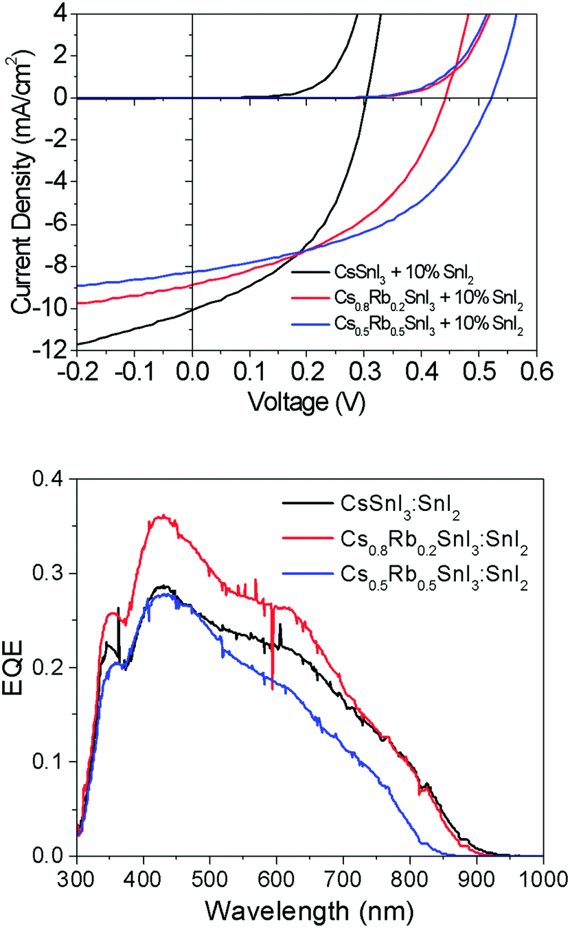 | ||
| Fig. 7 (upper) Representative current–voltage and corresponding external quantum efficiency (EQE) characteristics for devices made using Cs1−xRbxSnI3 + 10 mol% SnI2 for x = 0, 0.2, and 0.5 (lower) corresponding EQE spectra. | ||
However, the direction and magnitude of the change in Ip can be deduced on the assumption that the excess SnI2 is distributed in a similar way in all of the perovskite films, giving rise to a comparable perturbation of the surface potential contribution to the Ip measurement for all of the samples. Fig. 6 shows that substitution of Cs with Rb lowers the energy of the valence band edge with respect to the vacuum level (i.e. increases Ip) and the magnitude scales with increasing Rb content. Indeed, the magnitude of the change in Ip with increasing Rb content correlates closely with the increase in device Voc.
The change in band gap with Rb inclusion into the perovskite lattice is also evident from the change in device external quantum efficiency (EQE) spectra: Fig. 7(lower). It is estimated from the EQE spectrum for x = 0 and 0.2 (ESI,† Fig. S9(a)) that the band gap is increased by ∼ 20 meV for x = 0.2 which is in close agreement with the photoluminescence measurements (Fig. 5). Given that the magnitude of this increase is comparable to the thermal energy of an electron at room temperature it is barely significant, and so for x = 0.2 the energy of both the valence and conduction band edges must be decreased by approximately the same amount, enabling a significant increase in Voc of ∼120 meV with only a very small increase in band gap. For x = 0.5 the increase in band gap compared with x = 0 becomes significant, increasing by ∼160 meV from ∼1.34 to ∼1.5 eV. For x = 0.5 the change in energy of the low energy edge in the EQE spectrum is, again, in close agreement with the photoluminescence measurements. The reduction in device Jsc with increasing x can be partially explained by the differences in perovskite film coverage, which reduces from ∼98% for x = 0, to ∼94% for x = 0.2 and ∼84% for x = 0.5 (Fig. S7, ESI†). For x = 0.5 the significant reduction in band gap is also a plausible reason for the reduction in Jsc, since fewer long wavelength photons can be harvested.
To test the generality of this result, PV devices were also fabricated using perovskite films prepared using SnCl2 as the source of excess Sn and a PCBM ETL in place of C60 (Fig. 8), since we have previously shown that B-γ CsSnI3 devices using SnCl2 in conjunction with PC61BM achieves substantially higher fill factor and Voc, which is most pronounced after a few days storage in an inert atmosphere.8
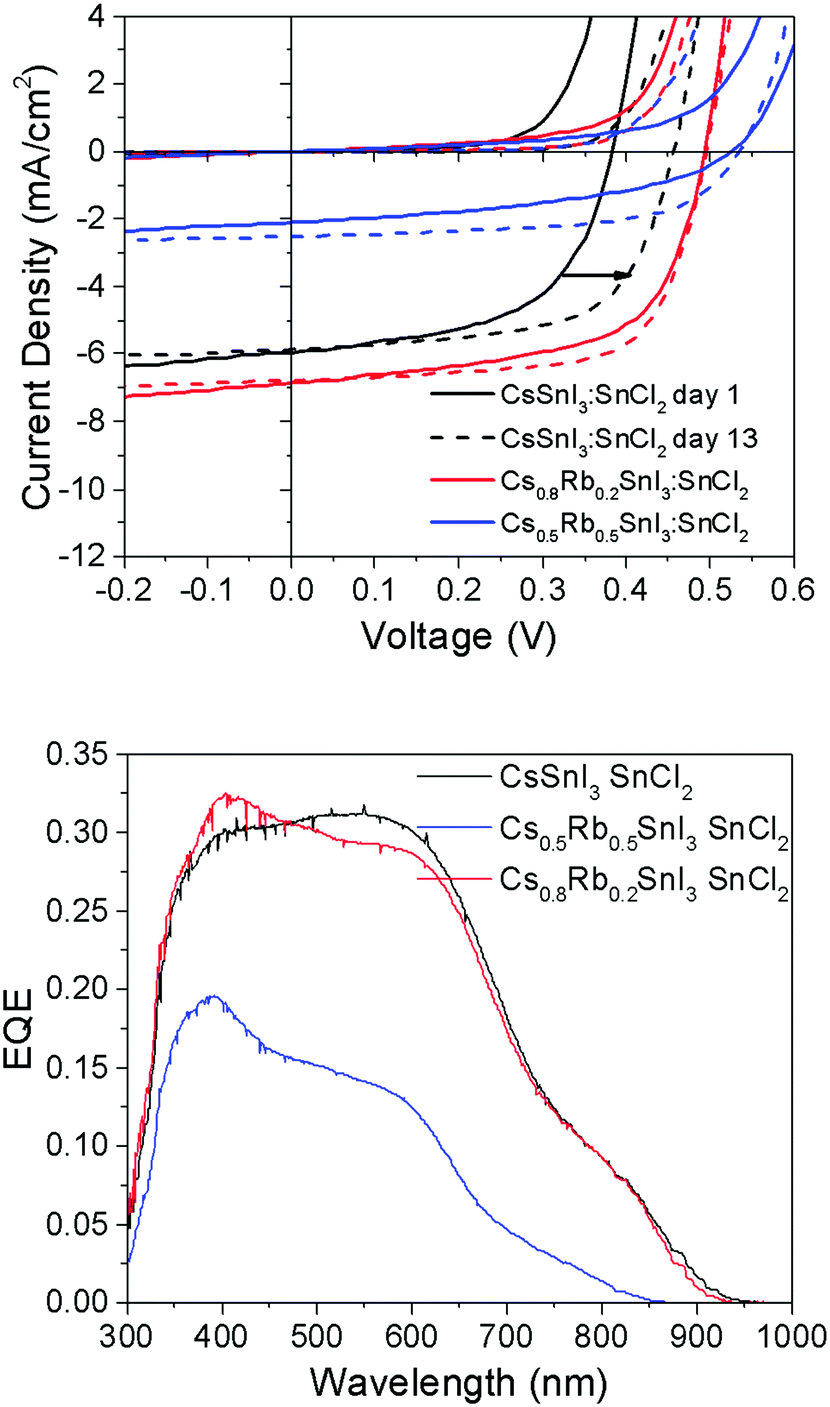 | ||
| Fig. 8 (upper) J–V characteristics of PV devices with the structure ITO|Cs1−xRbxSnI3 + 10 mol% SnCl2|PC61BM|BCP|Al (x = 0, 0.2 or 0.5) tested in the dark and under 1 sun simulated solar illumination immediately after fabrication (solid lines) and after 12 days storage under nitrogen (<1 ppm O2 and H2O) (dashed lines). Full data set given in ESI,† Table S3. (lower) Corresponding EQE spectra. | ||
It is evident from the data in Fig. 8 that the correlation between Voc and the Rb content for devices using SnCl2 as the source of excess Sn is consistent with that observed for devices using SnI2. For freshly made devices, the magnitude of the increase is in very close agreement (Table S3, ESI†): using SnI2 with x = 0.2 and 0.5 the increase in Voc is ∼120 mV and ∼170 mV respectively. Using SnCl2 with x = 0.2 and 0.5 the increase in Voc is ∼130 mV and ∼160 mV respectively. Interestingly, Fig. 8 and Table S3 (ESI†) show that the difference in Voc for devices with and without Rb incorporated into the perovskite lattice reduces from ∼130 mV to ∼90 mV after 12 days storage in an inert atmosphere due to an increase in the Voc of devices using CsSnI3, which does not occur in devices incorporating Rb. The reason why the Voc in devices with Rb incorporated into the perovskite lattice does not also exhibit an increase in Voc with storage time is not yet understood. However, it is important to note that for the case of Cs1−xRbxSnI3 prepared using SnCl2 as the source of excess Sn, the material system is complicated by the possible presence of Cs1−xRbxSnI3−yCly and/or phase separated RbSnCl3. Whilst the difference in Jsc for devices with 0% and 20% Rb substitution is small, consistent with the very small difference in band gap, the Jsc (Table S3, ESI†) for x = 0.5 Rb substitution is greatly reduced. The latter is attributed to partial decomposition of the perovskite film in situ in the device, since even with encapsulation under nitrogen films with x = 0.5 are unstable.
Conclusions
In summary we have shown that the 3-dimensional perovskite Cs1−xRbxSnI3 can be prepared from room temperature solutions of RbI, CsI and SnCl2 for x up to 0.5. Experiments and DFT simulations show that increasing Rb content simultaneously increases the band gap and reduces film stability, due to distortion of the lattice that occurs when Cs is partially substituted by the much smaller Rb cation at the A-site. We have shown that for small x (≤0.2) film stability is sufficient for utility as the light harvesting layer in inverted PV devices. When used in conjunction with the model electron transport layer; C60, a 120 meV increase in Voc was achieved for x = 0.2, which correlates closely with an increase in the perovskite ionisation potential. At the same time the increase in band gap for x = 0.2 is only ∼30 meV and so the light harvesting capability of the perovskite film is not significantly degraded. Consequently, if effective strategies can be developed for the passivation of this type of perovskite, similar to that needed for lead perovskites, then inclusion of Rb into the B-γ CsSnI3 perovskite offers an effective means of increasing the ionisation potential, and thus device Voc, without compromising light harvesting ability. Furthermore, we envisage that there is considerable scope for combining this strategy with halide ion substitution, which represents a fertile area for further research.Experimental
Materials
CsI (Sigma-Aldrich 99.9%), SnI2 (Alfa Aesar, 99.999%), SnCl2 (Sigma Aldrich, 99.99%), RbI (Alfa Aesar 99.8%), PC61BM (Solenne, 99.5%), C60 (nano-c, 99.9%), bathocuproine (BCP) (Alfa Aesar, 98%), N,N-dimethylformamide (DMF) (VWR, anhydrous, 99.8%), chlorobenzene (Sigma-Aldrich, anhydrous, 99.8%), acetone (Sigma-Aldrich, GPR, 99%), propan-2-ol (Sigma-Aldrich, GPR, 99.8%), deionised H2O (purite dispenser, >10 MΩ). CsI and non-anhydrous solvents were stored in air. All other chemicals were stored in a nitrogen filled glove box (<5 ppm O2 and <1 ppm H2O).B-γ CsSnI3 films
In a dry nitrogen filled glovebox CsI, RbI, SnI2 and tin(II) halide were mixed together in (1 − x):x:1:0.1 molar ratio. To this mixture N,N-dimethylformamide (DMF) was added to make an 8 wt% solution (total mass of solids), which was stirred overnight before use. To deposit films, two drops of solution were cast onto a substrate spinning at 4000 rpm for 60 seconds. The B-γ phase forms immediately upon solvent evaporation. For Cs0.5Rb0.5SnI3:SnI2, the film took several seconds to darken in colour after spin coating.
Device fabrication
Indium tin oxide (ITO) coated glass slides (Thin Films Devices Inc. 15 ± 3 Ω sq−1) were held in vertical slide holders and ultra-sonically agitated in an acetone bath, followed by a high purity water bath with a few drops of surfactant, followed by high purity deionized water only bath, and finally an isopropanol bath. After this, the slides were suspended in hot acetone vapour for 10 seconds before UV/O3 treatment for 15 minutes.Immediately after UV/O3 treatment the slides were transferred into a dry nitrogen filled glovebox for CsSnI3 film deposition, followed by deposition of a PC61BM film from 15 mg ml−1 chlorobenzene solution using a spin speed of 1500 rpm, or C60 which was deposited by thermal evaporation at a rate of 0.4 Å s−1 to a thickness of 40 nm. This was followed by thermal evaporation of 6 nm at 0.5 Å s−1 of bathocuproine (BCP) and then 50 nm of Al at 1 Å s−1. Thermal evaporation was performed at a pressure of ≤1 × 10⁻⁵ mbar (with substrate rotation). The Al electrode was deposited through a shadow mask to make six devices per slide, each with an area of 6 mm2.
PV device testing
Device testing was performed in the same glove box as used for device fabrication or, as for the stability testing, using a solar simulator outside the glove box. Current density–voltage (J–V) curves were measured using a Keithley 2400 source-meter under AM1.5G solar illumination at 100 mW cm−2 (1 sun), scanned from −1 V to +1 V at 0.1 V s−1. External quantum efficiency (EQE) measurements were carried out using a Sciencetech SF150 xenon arc lamp and a PTI monochromator, with the monochromatic light intensity calibrated using a Si photodiode (Newport 818-UV). The incoming monochromatic light was chopped at 180 Hz. For signal measurement a Stanford Research Systems SR 830 lock-in amplifier was used.J–V and EQE measurements were made using custom LabVIEW programs.
X-ray diffraction (XRD)
XRD was performed on thin films of CsSnI3 prepared from 16 wt% (total solids) DMF solution deposited onto a glass substrate (13 × 13 mm2) spinning at 4000 rpm for 60 seconds. A thicker film than used in the devices was used here to obtain sufficient signal for the time dependent studies. Measurements were made on a Panalytical X’Pert Pro MRD equipped with a hybrid monochromator (4-bounce Ge (220) monochromator and mirror combined) to give pure Cu Kα radiation and a solid state Pixcel detector. The sample was kept under a flow of gas (dry nitrogen, dry air, humid nitrogen or ambient air) using an Anton Paar DHS 1100 stage with a graphite dome. Simulated diffraction patterns were calculated using the program Mercury 3.122 using CIFs from the Inorganic Crystal Structure Database (ICSD)Powder X-ray diffraction patterns were analysed using the TOPAS software23 with the Pawley method used to fit the measured profile and refine lattice parameters.
X-ray/ultraviolet photoelectron spectroscopy
XPS was performed on film on gold coated glass substrates using a Kratos AXIS Ultra DLD. Samples were transferred using an inert atmosphere transfer arm from the nitrogen filled glovebox to the spectrometer ultra-high vacuum system and so were not exposed to the ambient environment. XPS measurements were carried out in a UHV system with a base pressure of 5 × 10⁻¹¹ mbar. The sample was excited with X-rays from a monochromated Al Kα source (hν = 1486.7 eV) with the photoelectrons being detected at a 90° take-off angle. Curve fitting was performed using the CasaXPS package, incorporating Voigt (mixed Gaussian–Lorentzian) line shapes and a Shirley background.UPS was performed in the same vacuum system as for XPS using a He 1α source at 21.22 eV.
Electronic absorption spectroscopy
UV/Vis/NIR spectra were measured for optically thin films of CsSnI3 on glass substrates. Experiments from the same set were performed on the same day. Measurements were made using Agilent Technologies Cary 60 spectrometers.Computational methods and structural models
The initial structure optimisations were performed using DFT within the local density approximation (LDA)24 as implemented in the Vienna ab initio simulation package (VASP).25 The exchange–correlation (XC) functional is used as parameterized by Perdew and Zunger.26 The outermost s, p, and d (in the case of Sn) electrons are treated as valence electrons whose interactions with the remaining ions is modelled by pseudopotentials generated within the projector-augmented wave (PAW) method.27 ESI,† Fig. S10 shows the crystal structures and unit cells used in the DFT calculations. Unit cells with 12, 20, and 36 atoms are used for the case of orthorhombic and yellow phase CsSnI3, and face centered cubic (FCC) Cs2SnI6 crystal structures, respectively. During the optimisation, the positions of the atoms, and the shape and volume of the unit cell are all allowed to relax. An energy cutoff of 500 eV and 6 × 4 × 6, 4 × 8 × 2, and 6 × 6 × 6 k-point meshes (for orthorhombic, yellow phase, and FCC structures, respectively) are used to achieve energy and force convergence of 0.1 meV and 2 meV Å−1, respectively.DFT–LDA underestimates the lattice parameters of the orthorhombic CsSnI3 by about 3%. The deviations of the band gaps (compared to those with experimental lattice constants) are in the range of Cs1−xRbxSnI3 about 250 meV to 350 meV when using LDA-optimized lattice constants. To be consistent, all the electronic structure calculations were performed with corrected lattice parameters by expanding the lattice parameters proportionally (to match experimental volume of the cells) while keeping the LDA-optimized shape of the cells. This procedure has shown to keep the ab initio aspects of the approach without compromising accuracy. The subsequent electronic structure calculations were performed using the DFT-1/2 method. The DFT-1/2 method stems from Slater's proposal of an approximation for the excitation energy, a transition state method,28,29 to reduce the band gap inaccuracy by introducing a half-electron/half-hole occupation. Ferreira et al.30 extended the method to modern DFT and particularly to solid-state systems. Recently, Tao et al.20 has reported the successful application of the DFT-1/2 method in predicting accurate band gaps of several metal halide perovskites including CsSnI3 with a calculated band gap of 1.33 eV. Fortunately, the computational effort is the same as for standard DFT, with a straightforward inclusion of spin–orbit coupling when coupled with VASP. In this work, the DFT-1/2 method with the same setting is used to looking at band gap evolution of Cs1−xRbxSnI3 by substituting Cs by Rb. The DFT simulations in Fig. 4 assume the following reaction pathway: 2Cs1−xRbxSnI3 + O2 → SnO2 + (Cs1−xRbx)2SnI6.
Conflicts of interest
There are no conflicts to declare.Acknowledgements
The authors would like to thank the United Kingdom Engineering and Physical Sciences Research Council (EPSRC) for funding (Grant number: EP/L505110/1 & EP/N009096/1). The authors also thank Adam Crocker and Edward Griffin (University of Warwick) who assisted with the collection of the photoluminescence measurements. All data supporting this study are provided as ESI,† accompanying this paper.References
- B. Wu, Y. Zhou, G. Xing, Q. Xu, H. F. Garces, A. Solanki, T. W. Goh, N. P. Padture and T. C. Sum, Adv. Funct. Mater., 2017, 27, 1604818 CrossRef.
- I. Chung, J.-H. Song, J. Im, J. Androulakis, C. D. Malliakas, H. Li, A. J. Freeman, J. T. Kenney and M. G. Kanatzidis, J. Am. Chem. Soc., 2012, 134, 8579–8587 CrossRef PubMed.
- Z. Chen, C. Yu, K. Shum, J. J. Wang, W. Pfenninger, N. Vockic, J. Midgley and J. T. Kenney, J. Lumin., 2012, 132, 345–349 CrossRef.
- L.-Y. Huang and W. R. L. Lambrecht, Phys. Rev. B: Condens. Matter Mater. Phys., 2013, 88, 165203 CrossRef.
- M. H. Kumar, S. Dharani, W. L. Leong, P. P. Boix, R. R. Prabhakar, T. Baikie, C. Shi, H. Ding, R. Ramesh, M. Asta, M. Graetzel, S. G. Mhaisalkar and N. Mathews, Adv. Mater., 2014, 26, 7122–7127 CrossRef PubMed.
- T.-B. Song, T. Yokoyama, S. Aramaki and M. G. Kanatzidis, ACS Energy Lett., 2017, 2, 897–903 CrossRef.
- K. P. Marshall, R. I. Walton and R. A. Hatton, J. Mater. Chem. A, 2015, 3, 11631–11640 Search PubMed.
- K. P. Marshall, M. Walker, R. I. Walton and R. A. Hatton, Nat. Energy, 2016, 1, 16178 CrossRef.
- K. P. Marshall, M. Walker, R. I. Walton and R. A. Hatton, J. Mater. Chem. A, 2017, 5, 21836–21845 Search PubMed.
- Q. Wang, X. Zheng, Y. Deng, J. Zhao, Z. Chen and J. Huang, Joule, 2017, 1, 371–382 CrossRef.
- Y. Yan, Nat. Energy, 2016, 1, 15007 CrossRef.
- I. Chung, B. Lee, J. He, R. P. H. Chang and M. G. Kanatzidis, Nature, 2012, 485, 486–489 CrossRef PubMed.
- J. Endres, D. A. Egger, M. Kulbak, R. A. Kerner, L. Zhao, S. H. Silver, G. Hodes, B. P. Rand, D. Cahen, L. Kronik and A. Kahn, J. Phys. Chem. Lett., 2016, 7, 2722–2729 CrossRef PubMed.
- D. Sabba, H. K. Mulmudi, R. R. Prabhakar, T. Krishnamoorthy, T. Baikie, P. P. Boix, S. Mhainsalkar and N. Mathews, J. Phys. Chem. C, 2015, 119, 1763–1767 Search PubMed.
- L. Lang, J.-H. Yang, H.-R. Liu, H. J. Xiang and X. G. Gong, Phys. Lett. A, 2014, 378, 290–293 CrossRef.
- Y. K. Jung, J. H. Lee, A. Walsh and A. Soon, Chem. Mater., 2017, 29, 3181–3188 CrossRef PubMed.
- R. Prasanna, A. Gold-Parker, T. Leijtens, B. Conings, A. Babayigit, H. G. Boyen, M. F. Toney and M. D. McGehee, J. Am. Chem. Soc., 2017, 139, 11117–11124 CrossRef PubMed.
- C. Li, X. Lu, W. Ding, L. Feng, Y. Gao and Z. Guo, Acta Crystallogr., Sect. B: Struct. Sci., 2008, 64, 702–707 CrossRef PubMed.
- G. Thiele and B. R. Serr, Z. Kristallog., 1995, 210, 64 Search PubMed.
- S. X. Tao, X. Cao and P. A. Bobbert, Sci. Rep., 2017, 7, 14386 CrossRef PubMed.
- B. W. Larson, J. B. Whitaker, X.-B. Wang, A. A. Popov, G. Rumbles, N. Kopidakis, S. H. Strauss and O. V. Boltalina, J. Phys. Chem. C, 2013, 117, 14958–14964 Search PubMed.
- C. F. Macrae, I. J. Bruno, J. A. Chisholm, P. R. Edgington, P. McCabe, E. Pidcock, L. Rodriguez-Monge, R. Taylor, J. Van De Streek and P. A. Wood, J. Appl. Crystallogr., 2008, 41, 466–470 CrossRef.
- A. A. Coelho, J. Appl. Crystallogr., 2000, 33, 899–908 CrossRef.
- W. Kohn and L. J. Sham, Phys. Rev., 1965, 140, A1133 CrossRef.
- G. Kresse and J. Furthmüller, Comput. Mater. Sci., 1996, 6, 15–50 CrossRef.
- J. P. Perdew and A. Zunger, Phys. Rev. B: Condens. Matter Mater. Phys., 1981, 23, 5048–5079 CrossRef.
- G. Kresse and D. Joubert, Phys. Rev. B: Condens. Matter Mater. Phys., 1999, 59, 1758–1775 CrossRef.
- J. C. Slater, Advances in Quantum Chemistry, Academic Press, 1972, vol. 6, pp. 1–92 Search PubMed.
- J. C. Slater and K. H. Johnson, Phys. Rev. B: Condens. Matter Mater. Phys., 1972, 5, 844–853 CrossRef.
- L. G. Ferreira, M. Marques and L. K. Teles, Phys. Rev. B: Condens. Matter Mater. Phys., 2008, 78, 125116 CrossRef.
Footnote |
| † Electronic supplementary information (ESI) available. See DOI: 10.1039/c8qm00159f |
| This journal is © the Partner Organisations 2018 |