
Application of ordered nanoparticle self-assemblies in surface-enhanced spectroscopy
Jiaming
Chen†
a,
Longhua
Guo†
 a,
Bin
Qiu
a,
Zhenyu
Lin
*a and
Tie
Wang
*b
a,
Bin
Qiu
a,
Zhenyu
Lin
*a and
Tie
Wang
*b
aInstitute of Nanomedicine and Nanobiosensing, MOE Key Laboratory for Analytical Science of Food Safety and Biology, Fujian Provincial Key Laboratory of Analysis and Detection Technology for Food Safety, College of Chemistry, Fuzhou University, Fuzhou, 350116, China. E-mail: zylin@fzu.edu.cn
bBeijing National Laboratory for Molecular Sciences, Key Laboratory of Analytical Chemistry for Living Biosystems, Institute of Chemistry, The Chinese Academy of Sciences, Beijing 100190, China. E-mail: wangtie@iccas.ac.cn
First published on 20th February 2018
Abstract
Surface-enhanced spectroscopy (SES), including surface-enhanced Raman spectroscopy (SERS), surface-enhanced infrared absorption (SEIRA), surface-enhanced fluorescence (SEF), surface-enhanced hyper-Raman spectroscopy (SEHRS), surface-enhanced second harmonic generation (SESHG), and surface-enhanced electrochemiluminescence (SEECL), is an emerging subject that has received significant attention from the research community over the past 40 years. The confined and strong enhanced electromagnetic fields generated from the surface of noble metal nanostructures are considered as the main cause of SES. More importantly, it has been proven that SES is strongly related to the orientation and inter-nanoparticle coupling of different nanostructures. This review article mainly focuses on the application of ordered nanoparticle self-assemblies in SES. Different strategies for the fabrication of ordered nanoparticle self-assemblies, the mechanisms of SES, and the application of SES have been reviewed in detail.
 Jiaming Chen | Jiaming Chen is a PhD candidate at the College of Chemistry at Fuzhou University. His research interests focus on surface-enhanced Raman scattering (SERS) and the fabrication of different functional nano-optical devices for rapid SERS detection. |
 Longhua Guo | Longhua Guo is currently a full professor at the College of Chemistry at Fuzhou University. He obtained his PhD from Fuzhou University in 2009. He then worked as a postdoctoral research fellow at the School of Chemical and Biomedical Engineering, Nanyang Technological University, from 2009 to 2011. He then joined the Ministry of Education Key Laboratory for Analytical Science of Food Safety and Biology (Fuzhou University) and has worked there since 2011. His research interests focus on the fabrication of nano-optical-based analytical devices for environmental and biological applications. |
 Tie Wang | Tie Wang is a professor at the Institute of Chemistry, Chinese Academy of Sciences (ICCAS). He received his BSc (2002) from Xi’An Jiaotong University and PhD (2007) from Changchun Institute of Applied Chemistry, China. Then he worked as a postdoctoral fellow at the Rensselaer Polytechnic Institute, Troy, NY, and the University of Florida, Gainesville, FL, both USA. He joined ICCAS and was awarded the “Thousand Youth Talents Plan” in 2013. His research focuses on nanoparticle assemblies and their applications. |
1. Introduction
Where to go for inspiration? Perhaps the best answer should be nature. Over billions of years, organisms in nature have evolved a variety of biological forms, which display many miraculous biological phenomena and mysteries. Among these, ordered micro- and nanostructures are abundant in biological systems, which exhibit remarkable performance including in optics and sensing.1–3 Many insects, such as mosquito, have compound eyes composed of a large number of integrated optical units called ommatidia1,4,5 (Fig. 1a and b). Compound eyes can improve the sensitivity of light vision because of the final periodic compound eye structure. Coincidentally, unique features of ordered microstructures in nature can be observed, including the colourful feather or wings of some butterflies, which result from the ordered arrangement and arrays of vertically aligned net-like skeleton structures.6–9 Moreover, these ordered micro- and nanostructures can contribute to form a fine sensing system of higher sensitivity, like in the silk moth Bombyx mori, which has hundreds of sensilla on the surface of the antennal branches of one of its antennas.10,11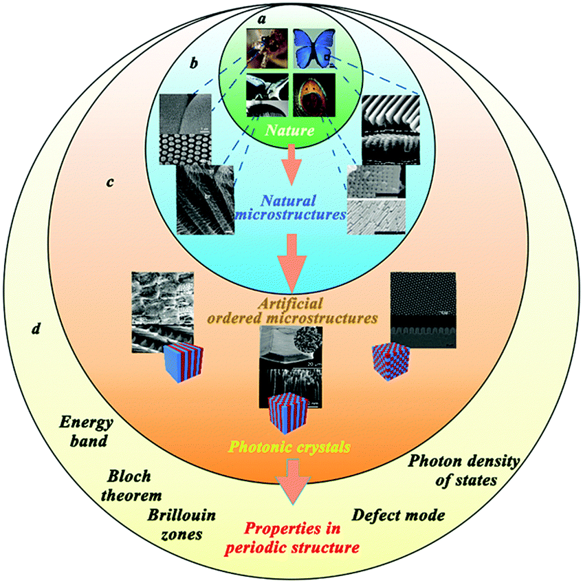 | ||
| Fig. 1 (a) Many creatures in nature have gorgeous colors and outstanding senses, which are based on some special microstructures of their organs; (Reprinted from ref. 5 and 8–11; Copyright 2007, John Wiley and Sons; Copyright 2003, National Academy of Sciences; Copyright 2012, John Wiley and Sons; Copyright 2005, John Wiley and Sons.) (b) SEM images of the organs’ microstructures from the creatures in (a). These special organs are made of ordered and sophisticated microstructures. (c) Various bio-inspired photonic structures have been explored, which can be summarized into photonic crystals in three orthogonal directions. (Reprinted from ref. 1, 6 and 10; Copyright 2012, John Wiley and Sons; Copyright 2009, John Wiley and Sons; Copyright 2006, American Chemical Society.) (d) Based on the periodic structures of these photonic crystals, concepts, like the Bloch theorem, energy band, and Brillouin zones, can be applied to photonic crystals; simultaneously, introducing the defect mode into the photonic band gap and modifying the photon density of states in the photonic crystals can influence the optical characteristics. | ||
In some cases, these abovementioned examples exhibit sophisticated and hierarchic photonic structures, which can provide researchers an ideal reference point. Inspired by nature, various materials and optical devices have been explored to achieve desired optical features. These materials and devices have similar periodic structures, such as multilayer structures, cylinder arrays or stacking spheres, which can be defined as photonic crystals in three orthogonal directions12 (Fig. 1c). Similar to the propagation of electrons through a periodic arrangement of atoms, the propagation of light occurring in the photonic crystals can be discussed using a similar explanation such as Bloch theorem or by the energy band and Brillouin zones. Additionally, the defect mode is an important concept that appears in the photonic band gap. When photonic crystals are applied to devices and sensors, and when the defect mode wavelength and the emission wavelengths of the active probes (dye or quantum dots) match, emission can be enhanced, due to a change in the density of states in the defect mode. Photonic crystals can be modified by changing the photon density of states; where the photon density of states can affect the optical response of active species near the photonic crystals12,13 (Fig. 1d). Notably, these photonic crystals have remarkable potential in optical spectroscopy and surface-enhanced spectroscopy. With the development of nanomaterial sciences, photonic crystals have gained more and more attention.
In the past decades, the development of nanotechnology has attracted considerable attention.14–16 The properties that nanoparticles exhibit differ from those of natural bulk samples of the same materials. This aspect has captivated researchers in various fields and seemingly provides almost unlimited promise. Besides the synthesis of individual nanostructures, the focus on nanotechnology extends to organizing the nanoparticles into an ordered and controllable formation. It is a great challenge for researchers to go from the macroscopic bulk cases to microscopic particles, then back to the macroscopic superstructures under scientific conditions, but undoubtedly, achieving controlled approaches for organizing such “building blocks” of tiny particles to construct specially designed structures would offer great potential for many applications. What has emerged in this aim is the self-assembly of nanoparticles which offers an effective and promising method for controlling the fabrication of superstructures with unique effects induced by the collective interaction of excitation, electromagnetic, optical and other coupling surface plasmons.15 In particular, these ordered self-assemblies display electronic, magnetic and optical properties, resulting in their great potential in different fields, including plasmon sensors, photocatalysis and applications of surface-enhanced spectroscopy (SES).
Surface-enhanced spectroscopy is an emerging branch of spectroscopy that combines plasmonic nanostructures and spectroscopy. Since 1974, a tremendous enhancement of Raman scattering was observed by Fleischmann et al.17 from pyridine absorbed on a roughened silver electrode. Surface-enhanced Raman spectroscopy (SERS) has become the subject of intensive study and an effective enhanced method for the application of Raman in widespread areas. In addition, after the SERS effect was discovered, surface-enhanced hyper-Raman spectroscopy (SEHRS),18,19 surface-enhanced fluorescence (SEF),20,21 surface-enhanced second harmonic generation (SESHG),22–24 surface-enhanced infrared absorption (SEIRA),25–27 surface-enhanced electrochemiluminescence (SEECL)28–33 and other enhanced spectroscopies have emerged as powerful techniques, collectively known as surface-enhanced spectroscopy (SES), for the study of surface phenomena and the interactions between molecules and nanoparticles. A series of surface-enhanced spectroscopies were observed that have similarities in their mechanisms and effects, especially relying on the collective effects of nanoparticles. Numerous experiments have demonstrated that assemblies of nanoparticles generate coupling plasmons that can be used to further improve the performance of surface-enhanced spectroscopy. Current interests in the assemblies of nanoparticles focus on organizing the nanoparticles into an ordered geometry and developing the effects based on these assemblies that give rise to the sensitivity and reproducibility of these spectroscopies.
Herein, we start by categorizing the main driving forces and strategies of nanoparticle assemblies for constructing plasmonic nanostructures. Then, a theoretical paradigm of plasmon and coupling plasmon is briefly provided. Moreover, the similarities and differences among SERS, SEF and SEIRA based on plasmonic nanostructures are discussed. Finally, we review some recent works on the applications of nanoparticle assemblies for surface-enhanced Raman spectroscopy, speculating about ordered nanoparticle self-assemblies in future scientific research and technological applications.
2. Mechanisms and strategies of ordered nanoparticle assemblies
Self-assembly is depended on several key issues, including the interparticle weak forces, the properties of individual nanoparticles (size distribution/shape), the modified ligands and the assisted external methods. These interactions between nanoparticles, such as van der Waals force, electrostatic force, hydrophobic interaction and so on, are the common driving forces in the self-assembly process.34 The different interactions are considered as one of the fundamental mechanisms that lead to individual nanoparticles self-assembling into diverse nanostructures.35 In some cases, there is not only one interaction existing in an assembly process, multiple interactions in assembly can exist in a complex and interdependent manner. The layering of molecules (surfactant, ligand or biomolecules), usually capped around colloidal nanoparticles, can be used for controlling the aggregation process in a solvent.36 Thus, the interactions and modified molecules play important roles in the particles or particle/environment. In addition, the size and shape of individual nanoparticles can influence the structure and morphology of assemblies.37Based on these factors and mechanisms, various strategies have been developed for fabricating ordered and plasmonic nanostructures. Herein, we give a brief illustration of the main interactions and the related issues, which may help us to review the mechanism and strategies of self-assembly.
2.1 Driven forces in self-assembly
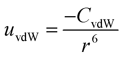 | (1) |
To understand and calculate the vdW force, different theories have been proposed. Among these, for spherical particles with a smooth surface, a simple and ideal model was used by Haymaker in 1937 to estimate the vdW force between pairs of atoms located within two particles; whereby the van der Waals' interaction energy between spherical bodies of radii R1 and R2 and with smooth surfaces could be approximated by:40
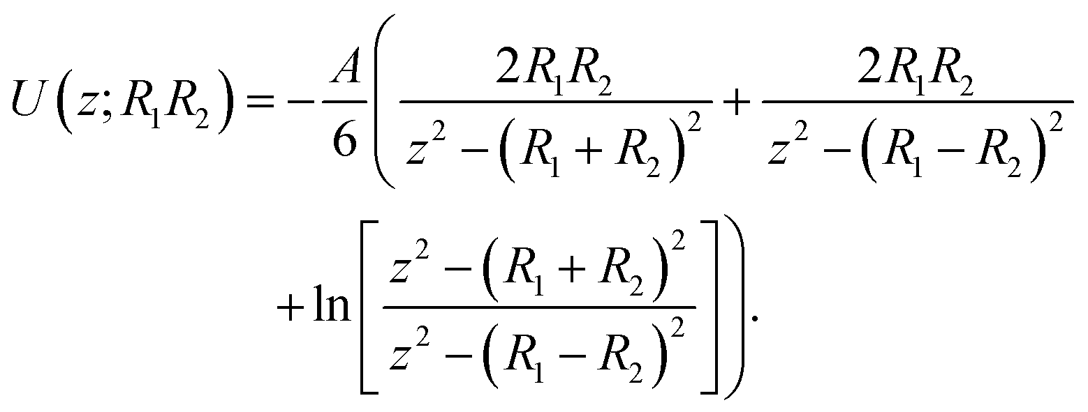 | (2) |
| z = R1 + R2 + r | (3) |
Eqn (2) for the potential energy function can be simplified to:
 | (4) |
The vdW-force-driven self-assembly, like the drop-evaporation method, induces the nanoparticles to form close-packed structures. Monolayer or multilayer superlattices have been obtained by vdW-force-driven self-assembly.43,44 By using the vdW force, close-packed monolayer or multilayer superlattices can be organized37,78 (Fig. 2). The droplet-evaporation method based on vdW force is widely used for the fabrication of close-packed superstructure assemblies. To highly control the geometry of a gold superlattice, the assembly procedure was carefully monitoring by tuning the experimental parameters, namely, the dispersing solvent, deposition temperature, gold nanoparticle (Au NP) concentration and chemistry of the supporting substrate.44,45 The short-range interactions, such as vdW forces, contribute to the formation of the superstructure. Also, the capping agent chain length and composition, size and concentration ratio can strongly affect the final geometry.46,47
 | ||
| Fig. 2 Self-assembly of close-packed monolayer and multilayer superlattices by using van der Waals forces. SEM images of monolayer superlattices: (a) octahedral gold nanocrystals; (b) cubic gold nanocrystals. (Reprinted from ref. 37; Copyright 2011, John Wiley and Sons) SEM images of multilayer superlattices: (c) top view of gold nanorods. (d) Side view of gold nanorod superlattices with 14 layers. (Reprinted from ref. 78; Copyright 2009, John Wiley and Sons.) (e) Self-assembled rhombic dodecahedral gold nanocrystals. (Reprinted from ref. 37; Copyright 2011, John Wiley and Sons.) | ||
 | ||
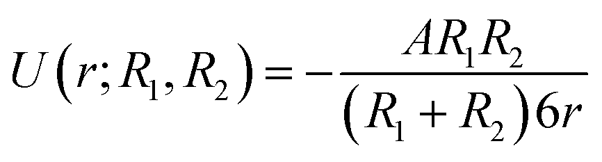
| Fig. 3 Self-assembly of a core–satellite structure by using electrostatic forces. (a) Schematic showing the steps involved in the self-assembly of core–satellite clusters. (b) TEM images showing different sizes of gold nanoparticles, which are employed as the core and satellites. (c) TEM images showing the successful assembly of core–satellite structures. (Reprinted from ref. 53; Copyright 2012, American Chemical Society.) | ||
 | ||
| Fig. 4 Nanoparticle self-assemblies by using other driving forces. (a) Schematic illustration of the fabrication of gold nano-dimers by using DNA-directed self-assembly. (Reprinted from ref. 54; Copyright 2013, American Chemical Society.) (b) Using increasingly hydrophobic Ag octahedra for self-assembly with various thiols, resulting in the different formations of superlattices. (Reprinted from ref. 55; Copyright 2015, Springer Nature.) | ||
2.2 Shape effects for tuning the morphology of nanoparticle assemblies
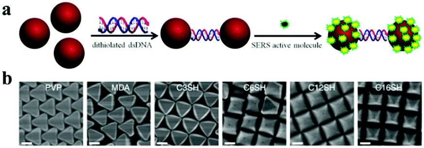
Recent nanotechnology advances can provide nanoparticles of various sizes, shapes and dimensions, which is regarded as an opportunity to use them for fabricating the ordering of nanomaterials.56,57 For different purposes, designing and fabricating a suitable morphology of nanoparticle assemblies is necessary.58The nanospheres or quasi-spherical nanoparticles are the simplest and the most common nanoparticles used as building blocks to construct more complex nanostructures. Simply, nanospheres can self-aggregate into many diverse structures, including dimers, trimers and larger number aggregates of nanospheres, which can then be applied for nanoprobes or nanotags.59 With the aggregating number increasing, larger nanoparticle aggregates, such as nanochains or even monolayer and multilayer superstructures, can be achieved60–66 (Fig. 5). Due to the symmetry of a nanosphere, the geometrical morphology of the assemblies is oriented with a close-packed plane, which results in the formation of fcc (face-centred cubic) and hcp (hexagonal close-packed) structures.35 In addition to the shape effect of nanoparticles, the surface ligands also play a key role in the formation of a superlattice.67 These close-packed nanostructures are widely used in fabricating enhanced substrates, because of the unique optical properties, and for coupling plasmon nanostructures. Notably, the close-packed structures have excellent sensitivity and reproducibility in surface-enhanced spectroscopies based on the short-range interparticle gap.68
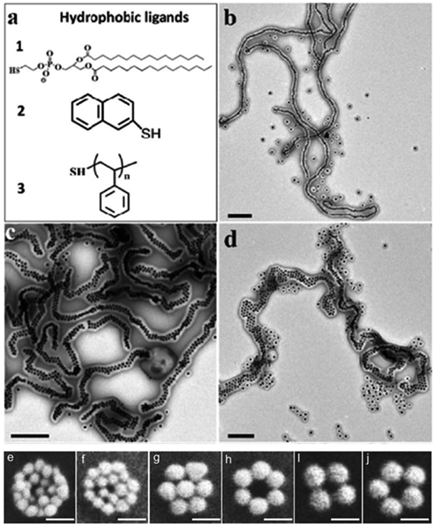 | ||
Fig. 5 Nanochains and nanoclusters, which aggregate with the increasing number of nanoparticles. (a) Chemical structures of three hydrophobic ligands 1–3. (b–d) TEM images of the single-, double- and multiple-line chains obtained in DMF/H2O = 7![[thin space (1/6-em)]](https://www.rsc.org/images/entities/char_2009.gif) :3 solution and after purification, where (b) 1 = stabilized AuNPs, (c) 2 = AuNPs, (d) 3 = AuNPs coated in PS154-b-PAA49 shells used as the monomers. (Reprinted from ref. 66; Copyright 2014, American Chemical Society.) (e–j) SEM images of individual gold nanoclusters with different diameter values and numbers; all the size bars are 100 nm. (Reprinted from ref. 65; Copyright 2010, John Wiley and Sons.) :3 solution and after purification, where (b) 1 = stabilized AuNPs, (c) 2 = AuNPs, (d) 3 = AuNPs coated in PS154-b-PAA49 shells used as the monomers. (Reprinted from ref. 66; Copyright 2014, American Chemical Society.) (e–j) SEM images of individual gold nanoclusters with different diameter values and numbers; all the size bars are 100 nm. (Reprinted from ref. 65; Copyright 2010, John Wiley and Sons.) | ||
By contrast, rod-shape nanoparticles have anisotropy so that they commonly exhibit two formations: ss (side-by-side) and ee (end-to-end). Generally, nanorods are organized to produce a variety of structures, ranging from a simple dimer to a chain, in the ss or ee form.69 Additionally, rod-shaped nanoparticles can be assembled into superstructures.70,71 There are more changes in close-packed nanorod assemblies than possible in nanosphere assemblies.67,72 Close-packed rod-shaped nanoparticle assemblies can be categorized as a crystal, liquid crystal and more complex three-dimensional geometries, such as a needle-like shape.71 Noteworthily, vertical arrays of nanorods have been observed to assemble into the close-packed formation of hcp.73,74 Furthermore, other anisotropic nanomaterials, which have a two-dimensional pattern, like a triangle, square or hexagon of the cross-section, can be assembled into ordered nanostructures for maximization of the tiling density75 (Fig. 6).
 | ||
| Fig. 6 The two different formations: ss (side-by-side) and ee (end-to-end), of self-assembly of rod-shape nanoparticles. TEM images of hybrid cylindrical micelles formed from PS51k-b-P4VP18k (PDP)2.0 with various NRs (diameter, 6 nm; length, 12 nm) content: (a and c) 11 vol%; (b and d) 21 vol%, resulting in ss and ee, respectively. (Reprinted from ref. 69; Copyright 2013, American Chemical Society.) (e) SEM image of a gold nanorod array. (f) SEM image recorded at a tilt angle of 52°. (Reprinted from ref. 74; Copyright 2012, John Wiley and Sons.) | ||
Additionally, the self-assembly of two nanoparticle species is also possible, rather than forming just size- and shape-uniform nanoparticles. The mixtures of nanoparticle shapes include spheres with spheres, spheres with rods, spheres with plates and so on, which is discussed in Section 2.3.4.
2.3 Strategies for the fabrication of plasmon nanostructures
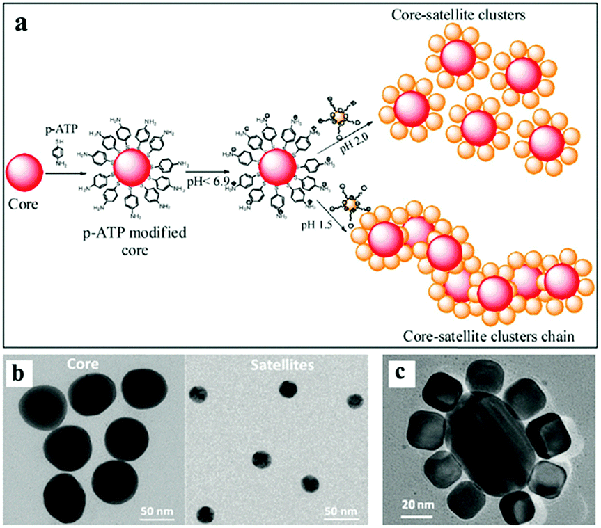
To obtain the desired structures and functionalities of nanoparticles, various strategies and rules employing diverse shapes and different interactions, functional molecules and other external assisted methods have been extensively studied.76DNA strands are perhaps the most versatile surface ligands for finely controlling nanoparticle assemblies.77 Different structures can be assembled by varying the oligonucleotide sequence,81 while at the same time the experimental procedure remains unchanged (Fig. 7). Basically, the assembly scheme starts with the particles, which are functionalized with two pre-designed complementary single strands, respectively. A following hybridization of the complementary DNA strands leads to the assembly of the nanoparticles.82,83 It was demonstrated that weak forces, like hydrogen bonding, electrostatic and hydrophobic interactions, cooperatively drive one DNA strand to assemble with its complement into a double helix. In these ways, extended assemblies, such as 2D or 3D nanoparticle aggregates, can be obtained.77,84,85 Therefore, DNA-based self-assembly is emerging as a useful tool using a highly promising template for organizing nanomaterials in a pre-designed way.
 | ||
| Fig. 7 Schematic of how plasmonic nanoparticle assemblies can be designed and synthesized by using DNA nanotechnology and a range of plasmonic nanostructures. (Reprinted from ref. 81; Copyright 2011, Springer Nature.) | ||
In addition to the DNA linkers, some biomolecules based on enzyme-linked immunosorbent assay (ELISA) have been used as the linker for the conjunction of nanomaterials.86 These biomolecule linkers, such as an antibody with antigen, biotin with streptavidin, a virus and protein, exhibit excellent specific binding for self-organized aggregation.79
Besides these biomolecular ligands, polymers, as versatile and diverse functional ligands, also play an important role in surface modification.87 Utilizing polymer and polymer properties can enable obtaining not only polymer functional nanoparticle composites but also polymer-nanoparticle assemblies. Many polymers, such as linear, branched and block copolymers, have been applied for the process of self-assembly. These polymer-nanoparticle assemblies can be tuned based on the polymer's molecular weight, chemical nature, architecture, persistence length and surrounding solvent for obtaining pre-designed geometrical morphologies.79 Generally, most of polymer-nanoparticle assemblies can follow three strategies: (1) assembly of the polymer-media nanoparticles into aggregates (e.g. tuning the aggregating by utilizing dendrimers of different generations88), (2) utilizing the polymer as a matrix to induce nanoparticles into an ordered and anisotropic oriented formation (e.g. nanoparticles grafted with polystyrene and orderly embedded in a polystyrene matrix89) or (3) acting as a functional element (e.g. possessing an electronic property90).
In most cases, surfactants have been utilized as surface stabilizers or templates in the synthesis of nanoparticles. The research evidence has demonstrated that an excess of surfactant is beneficial for ordered superlattice structures by controlling the dewetting of the solvent.91 In the droplet-evaporation self-assembly process, these surfactants, such as cetyltrimethylammonium bromide (CTAB), play a key role in the formation of ordered superstructures.92 Generally, this approach is simply done by casting a droplet of the nanoparticle solution onto a solid support (e.g. a glass slide or silicon wafer) and keeping it at a controlled temperature and humidity until it is dried.92 Besides surfactants, the effect of ions makes a contribution to the nanoparticle aggregation during the process of solvent evaporation, and can lead to a change in the surface charge of the nanoparticles.49 A salt (e.g. sodium chloride) can be added into the nanoparticle solution for the aggregation, and this reduces the stabilizing energy barrier in the interaction potential between charge-stabilized colloidal particles.93
Oil–water interfacial self-assembly was employed for organizing particles to fabricate larger nanostructures at the oil–water interface, which was based interactions of the surface ligands of nanoparticles and their environment.94,95 This liquid–liquid assembly, analogous to the case of Pickering emulsions, can generate a resistant film at the interface between two immiscible phases.96 For example, Wang and co-workers55 assembled three wafer-scale 2D plasmonic superlattices at the oil–water interface by tailoring the surface chemistry of Ag octahedra. Tuning the solvent and the ligands can strongly influence the shape of the final nanostructures at the interface, which is an effect driven by the reduction in interfacial energy55,97–99 (Fig. 8).
 | ||
| Fig. 8 Different strategies of interfacial self-assemblies. (a) Schematic of the steps involved in the interfacial self-assembly at the oil–water interface by controlling the surface wettability of Ag octahedra. (Reprinted from ref. 55; Copyright 2015, Springer Nature.) (b) Cross-section of the three-phase interface (left). Schematic representation of the stages of film formation of the Ag nanowires at the three-phase interface (right). (Reprinted from ref. 94; Copyright 2010, John Wiley and Sons.) | ||
Applying an external field, like an electric field or magnetic field, can also facilitate the assembly of nanostructures. By the use of an external field, nanoparticles, especially the anisotropic sort, can be directly oriented from individual building blocks to ordered assemblies.100–102 Zhu et al. and co-workers controlled the assembly of polystyrene-tethered gold nanorods in anodic aluminium oxide channels by the assistance of an electric field.103 The electric field played a key role in determining the ordered assemblies, which provided the driving force to reorientate the anisotropic NRs. A magnetic field, analogously, can influence the orientation of magnetic nanoparticles (i.e. with a permanent or field-induced magnetic dipole moment).104 Wang et al. reported105 the synthesis of ellipsoidal colloidal particles with anisotropy in both morphology and magnetic properties, which were used as building blocks for assembling 3D ordered structures with unique tuneable photonic properties.
With the geometrically constrained features (e.g. pores, channels), different assembly patterns of nanostructures can be fabricated and controlled by the use of pre-designed templates.69,73,106,107 For example, nanorod arrays are extensively explored based on the nanoporous templates.108 Lithographic techniques have been used to create suitable topographical templates and patterns, which is beneficial for organizing prepared nanomaterials into designed structures. These spatially selective assembly of nanoparticles at the desired location can be achieved by an electrostatically mediated assembly of particles and confined deposition nanoparticles.109 Nepal et al. reported a method involving the assembly of gold nanorods on chemically nanopatterned surfaces with a simultaneous control of both the interparticle spacing and local orientation.110 The combination of different driving forces and lithographic techniques, such as capillary force, could organize nanostructures into ordered assemblies in the confined area.74,111 Flauraud et al. reported a method involving the insertion of nanorods into the traps as resilience against the receding suspension front, followed by drying of the residual solvent, which could deterministically direct the capillary assembly of Au nanorods to attain a simultaneous control of the position, orientation and interparticle distance at the nanometre level111 (Fig. 9).
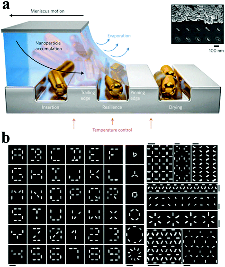 | ||
| Fig. 9 The strategy of evaporating self-assembly via a pre-designed template. (a) Schematic of the capillary assembly of nanoparticles onto topographical traps of a low-wetting substrate. The three sequential stages of capillary assembly are illustrated from left to right: nanoparticles are successfully assembled if they (1) are inserted into a trap, (2) are not removed from the trap by capillary doctor blading or by friction with the sliding accumulation zone and (3) withstand displacement and reorientation within the trap during the final solvent drying. (b) Examples of 2D patterns of Au nanorods fabricated by a topographically templated capillary assembly. All scale bars, 250 nm. (Reprinted from ref. 111; Copyright 2016, Springer Nature.) | ||
Simplex nanoparticle assemblies. Simplex nanoparticles, which have a similar composition and shape, can assemble into new organized assemblies. These ordered assemblies of nanoparticles not only exhibit the function of the individual nanoparticles, but also the collective physical effects from the integral superstructure. The forms of nanoparticle assemblies can be classified by the diversity of assemblies based on: non-dense-packed structures and dense-packed structures.
Non-dense-packed assemblies range from dimers of nanoparticles with different individual shapes to more complex and larger aggregates, such as chains and core–satellites. Most studies of these assemblies have been performed with regard to the structural control and the tuning of the interparticle distance, which provide the possibility to generate new properties that can be further used in optical sensing at the single nanostructure level. Dimers of nanoparticles are the most extensively studied among these assemblies, due to their simplex structure. Moreover, to attain the more complex assemblies, either nanochains or nanoclusters, the study of dimers as the basic unit is necessary. In the early stage, large electromagnetic field enhancements at the junctions were observed with pairs of spherical nanoparticles, when the surface plasmons are excited. The unique physical properties confined between the neighbouring nanoparticles have attracted plenty of attention. For the self-assembly of nanoparticles, most attempts have been done not only on the nanoparticle material, size and shape but also on the interparticle spacing, the number of nanoparticles and the structures of the assemblies.
Controlling the number and structures of particles for linear chains of metal nanoparticles, such as one-dimensional (1D) assemblies, offer novel means for exploring complex nanostructures and new properties.66,112 To effectively control the assemblies, surface modification of the nanoparticles is widely used. Barrow and co-workers made gold nanoparticles assemble into chains of differing lengths (1–6 particles) by using thiolated single strand oligonucleotides as a linker.113 Based on the experimental data, an exponential model was developed that allowed determination of the asymptotic maximum resonance at a chain length of 10–12 particles. More complex structures of clusters have also been designed, which are not confined to 2D forms. Nanoparticles as building blocks could be precisely fabricated into pre-designed 3D structures via molecular linkers, such as DNA, due to its highly customizable structure. For example, Tian et al.114 used the DNA origami octahedron as the frame to fabricate clusters with various symmetries and particle compositions. Notably, this work could be extended to designed arrangements of nanoparticles in 1D and 2D arrays by prescribing specific vertices of the octahedron as nanoparticle connecting sites.
The studies of nano-dimers have extended to other shapes of nanoparticles, such as rod-, cube- and prism-shaped, which exhibit more outstanding EM optical performances rather than the individual nanoparticles.
Binary nanoparticle assemblies. Different nanoparticles, which may have differences in the material, size and shape, can be assembled into so-called binary nanoparticle assemblies involving more complex structures. Studies of these binary nanoparticle assemblies have received relatively less attention compared to the simplex nanoparticle assemblies. On the other hand, multiple properties can be attained due to the different organization of assemblies.
Non-dense-packed assemblies are not only fabricated by particles with the same properties but also by different types. The blocks for these assemblies may have different properties from more than two types, such as the component, size and shape. Typically, heterocomponent dimers of gold and silver, silver and copper nanoparticles have been observed and explored in recent years.115 For example, Sheikholeslami and co-workers fabricated a silver/gold nanoparticle heterodimer via the DNA assembly method and systematically investigated the effects of symmetry breaking by scattering spectroscopy from single dimers.116 Lombardi et al. demonstrated the fabrication of asymmetric dimers formed from a gold nanoparticle bound to a silica-coated silver nanoparticle (Ag@SiO2 NP), which were separated with the silica shell of Ag@SiO2 NP.117 To achieve smaller gaps between these heterodimers, a DNA origami platform was used as a mediate linker to build a hetercomponent dimer that involved the same size (40 nm) gold and silver nanospheres by Weller et al.118 These asymmetric dimers open up many possibilities for nanoscale manipulation of the electromagnetic field and study of the collective plasmon modes by playing with the constituent particle composition, size, shape and interparticle distance (Fig. 10).
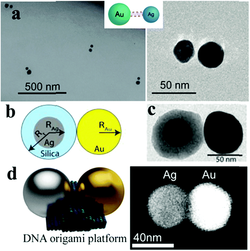 | ||
| Fig. 10 Schematic of an asymmetric nano-dimer. (a) TEM images of asymmetric dimers composed of a 30 nm silver nanoparticle and 40 nm gold nanoparticle. (Reprinted from ref. 116; Copyright 2010, American Chemical Society.) (b) Model morphology of an Au@Ag@SiO2 hetero-dimer formed by spherical particles. (c) TEM image of the investigated dimer formed by quasispherical particles with RAu = 29 nm, RAg = 20 nm and a SiO2 shell thickness Rt–RAg = 16 nm. (Reprinted from ref. 117; Copyright 2013, American Chemical Society.) (d) Schematic (left) and SEM image (right) of an individual Ag–Au heterodimer (backscatter contrast). (Reprinted from ref. 118; Copyright 2016, American Chemical Society.) | ||
Besides the heterodimers, satellite-shaped binary nanostructures can be assembled by two different types of nanoparticles with a larger number. Yoon and co-workers presented asymmetric core–satellite nanostructures built by a core gold nanoparticle (51 nm) and several smaller gold nanoparticles (13 ± 3 nm) as “satellites”.119 The gap between the satellites and core nanoparticle could be controlled by varying the length of the alkane dithiol linkers. Besides the use of small molecule linkers, core–satellite assemblies have also been built via DNA and hyperbranched polymer linkers, which allows programmable assembly.120–122 Similarly, different shapes of nanoparticle were assembled to give a core–satellite nanostructure. For example, Xu et al. utilized a gold nanorod and multiple nanospheres as the core and satellites of the nano-assemblies, respectively, to fabricate a core–satellite nanostructure.123 Based on the selective modification of nanorods with DNA oligomers, three types of assemblies with distinct elements of regiospecificity and high synthetic yield can be attained, which provides the possibility for multi-nanosphere, multi-nanorod superstructures with increased topological complexity and regiospecificity.
3. Principle of surface-enhanced spectroscopy on ordered nanoparticle assemblies
Since the discovery of SERS, surface-enhanced technology has already been applied to fluorescence, second harmonic generation and infrared absorption spectroscopies, which led to the development of a new subject called “surface-enhanced spectroscopy (SES)” that has been widely used in various fields in chemistry, physics, biology and new materials over the last 40 years.124–126 While some of the applications of SES may be surprising, the mechanisms of enhancement are still not clear at all, which captures the attention of researchers worldwide14 to investigate the mechanism of enhancement and the origin of these plasmons that play such an important role and which is closely related to the nanostructures. These nanostructures range from a single nanosphere, dimer or larger aggregates to monolayer or multilayer close-packed superstrucures.58The nanostructure-based optical properties, including scattering, absorption and extinction, lead to a variety of spectroscopic techniques.68,124 In particular, the enormous advances in nanotechnology have led to nanoparticles with a controllable size and shape, and complex aggregates and arrays in pre-designed geometrical shapes. For nanoparticle aggregates or arrays, it is possible for the plasmon resonances in each particle to be coupled, leading to shifts in the plasmon wavelengths or changes in the intensities. These effects are strongly influenced by the interparticles’ distance. In this case, one can combine plasmon-resonance effects in the nanoparticles with photonic resonance associated with the nanostructure to produce new coupling plasmon resonance.127 The coupling of nanostructures can also influence the spectroscopic intensities, leading to the possibility of photonic contributions to the enhancement effects in combination with plasmonic enhancements.58 Therefore, for better improving the performance of SES, understanding the relationship between SES and plasmons is necessary.
3.1 Localized surface plasmon resonance
From classical electromagnetism, internal polarization has been used for describing Maxwell's equations for media. Plasmon polaritons occur in a metal while the energy wave is shared between the electromagnetic field oscillations and the internal excitations of the medium. Common noble metals, such as Au, Ag, Cu and Pd, have exhibited remarkable optical properties and plasmon resonances.128 Additionally, other metals have demonstrated that they can generate plasmon resonance. For example, Al exhibited promising plasmon resonance at wavelengths ranging from deep-UV to NIR.129 On planar interfaces, surface plasmon polaritons (SPPs) can be simply viewed as electromagnetic surface modes that are relevant to an electromagnetic (EM) field and plasmonics, which are associated with smooth, thin films of silver and gold with thicknesses in the 10–200 nm range. Propagating surface plasmon polariton (PSPP) is found at boundaries between the dielectric and metal conductor. PSPP can propagate over relatively long distances on the surface, which opens up the possibility to make use of the mechanism to manipulate and guide light for the design of plasmonic chips. The coupling of light makes the SPPs sensitive to external parameters, which leads to sharp surface plasmon resonance (SPR).To understand, by way of analogy, the modes called localized surface plasmon polaritons (LSPs), involving small metallic particles instead of a planar surface, a simple model, involving a spherical metallic particle, was considered for better studying the electromagnetic (EM) field when molecules (probe or luminophore) are in the vicinity of particle. At the particle surface and its local area, the electromagnetic field strength increases, while the surface plasmon resonances are excited by the light. According to Mie theory, an approximation can help with the understanding of the physics involved. For a spherical metal nanoparticle with a size much smaller than the wavelength of light, the surface plasmon oscillation is dominated by the dipolar mode with a polarizability α given by:130,131
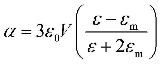 | (5) |
When the metallic particle is small to nanoscale, the LSPs of the nanoparticle can be excited by an incident wave, which then couple efficiently, resulting in a resonant optical response at the LSP frequency, with the appropriate polarization and frequency. Different from SPR, localized surface plasmon resonance (LSPR) is the collective oscillation of electrons within the nanostructures excited by incident light of a larger wavelength than the size of the nanostructure. The coherent oscillation results in strong light scattering and a unique surface plasmon absorption spectrum. The intensity and peak location of the absorption and scattering spectra are not only highly dependent on the composition, but also on the nanoparticle shape, size and the surrounding medium. For a spherical particle with radius a, the extinction efficiency for the dipole resonance is:132
 | (6) |
000 times greater in intensity than the incident field.
Note that, compared with spheres, the effect of shape is more complex. Even though spherical particles provide an excellent model system, some evidence has pointed out that some different shapes have stronger plasmon resonance for the electromagnetic field. These aggregates of nanoparticles, regarded as aggregated small spherical particles, exhibit remarkable enhancement for spectroscopy, like SERS.
3.2 Coupling plasmon resonances
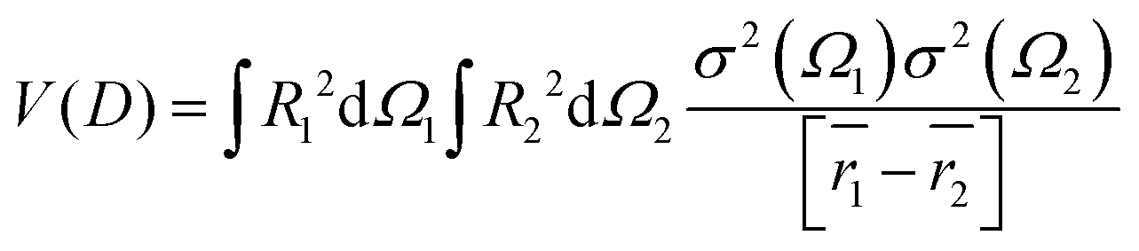
Various new designs of surfaces for enhancement have been studied, such as isolated particles, gratings, randomly roughened surfaces and assemblies of particles on surfaces.The dimer of spherical particles has served as the related simplest structure for studying the principle of plasmon coupling and the influence on spectroscopic enhancements. From these experiments, the dimer exhibited an enhancement of an intense and localized electromagnetic field. The collective oscillation of free electrons occurs in noble metal nanoparticle assemblies, resulting in an enhancement of the electromagnetic field at the junction regions (nanoscale gap), which are referred to as so-called hot spots. The coupling of EM fields strongly influences the optical properties of molecules and non-metal nanoparticles in the vicinity of the hot spots. The coupling of electromagnetic fields depends on the shape, arrangement of the nanoparticles and the interparticle spacing. A dimer of nanoparticles as the model can be used for better understanding the plasmon resonance:38,133
 | (7) |
 | (8) |
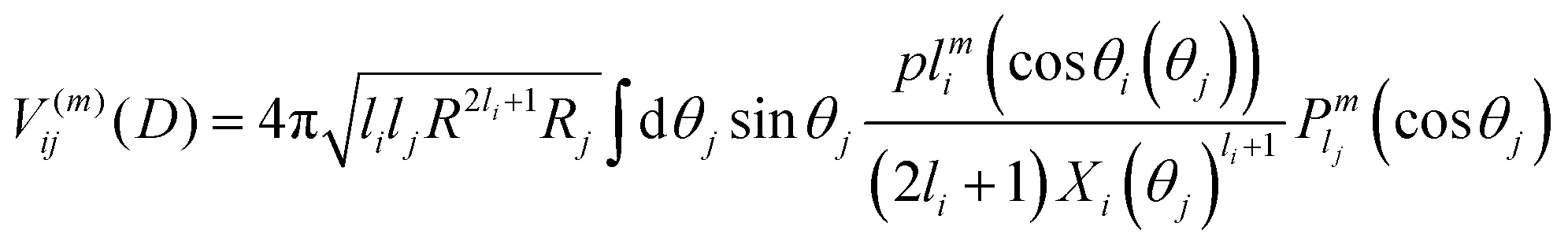
The interaction V(m)ij describes the coupling between two noninteraction plasmon modes i and j:
 | (9) |
Also, the incident light induced field is polarized along the axis of the dimer or transverse to the sphere, resulting in the LSPR intensity and shift (Fig. 11). When the coupling plasmon is extended to large-scale particle arrays or lattices, these types of nanostructures can exhibit a considerable strong field by varying the spacing, distribution and geometric of particles. Coupled dipoles can help us understand the coupling plasmon and optical properties.
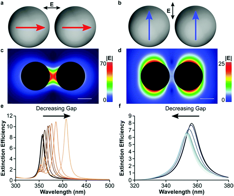 | ||
| Fig. 11 Plasmon coupling in spherical dimers with small gaps. (a) Constructive dipolar coupling in spheres with light polarized along the dimer axis. (b) Destructive interference between dipoles with light polarized across the dimer axis. Electric field intensity of constructively (c) and destructively (d) interfering 10 nm radius Ag spheres separated by a 5 nm gap. Extinction spectra of a 10 nm radius sphere Ag dimer with decreasing interparticle gaps with light polarized along (e) and across (f) the dimer axis. The interparticle gaps in (e and f) (from darkest to lightest trace) are 50, 40, 30, 20, 10, 5, 4, 3, 2 and 1 nm. The scale bar is 10 nm. (Reprinted from ref. 58; Copyright 2016, American Chemical Society.) | ||
When considering the coupled-dipole approximation, we consider an array of N particles whose positions and polarizabilities are denoted ri and αs. For a given wavelength λ, this field is:58,132
 | (10) |
 | (11) |
 | (12) |
 | (13) |
In the case of an infinite array of particles, it is possible to generate an analytical solution to eqn (5) for the case where the wave vector is perpendicular to the array axis (or plane). By assuming that the induced polarization in each array element is the same, this leads to the following expression for the polarization and extinction cross-section of each particle, respectively:
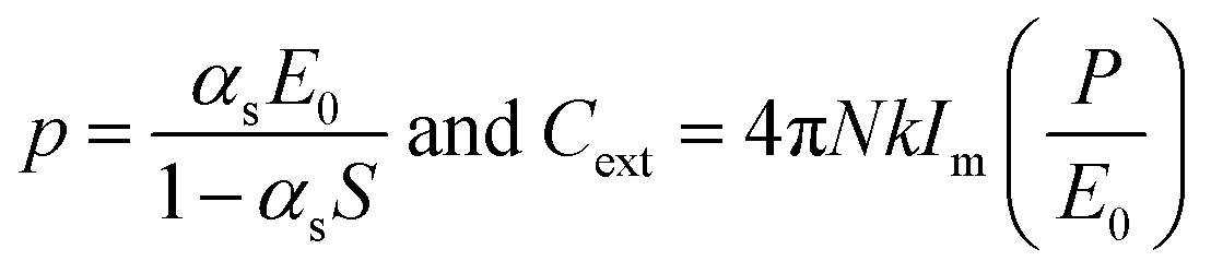 | (14) |
 | (15) |
Thus, the retarded dipole sum S greatly influences the optical properties of the array. Using the coupled-dipole approximation, a variety of interesting optical phenomena have been identified that can be controlled with the nanoparticle size, spacing and interparticle distance. As such, 2D arrays can provide enhanced sensing or detection opportunities due to the enhanced sensitivity of the lattice plasmon to changes in the dielectric environment of the particle and local fields, which are further amplified compared to the plasmon enhancement with isolated nanoparticles.
3.3 Electromagnetic field and optical effects
The electromagnetic field can be induced by the LSPR of noble metal nanoparticles and nanoparticle assemblies and some factors, like size, shape and arrangement.134,135 By using the discrete dipole approximation (DDA),132 it was found that the largest E2 value for an examined dimer was a factor of 10 larger than the for the monomer examined. For individual particles, Schatz and co-worker found that the largest E2 values were very similar for triangular prisms, oblate spheroids or cylindrical rods, with E2 always being less than 104. For a dimer of nanoparticles, we find E2 values closer to 105 for structures where the particle separation is 2 nm. Also, the enhancements are strongly dependent on the interparticle distance and the particle size.Noble metal nanoparticles interact remarkably with the EM field and their plasmonic resonance frequencies are located in the visible light region due to the d–d band transitions.136 From the absorption spectra, a decrease in the plasmon resonance band intensity and an increase in bandwidth with decreasing particle size can be seen.137 As the silver nanoparticles are assembled into a monolayer, the plasmon-resonance peak is shifted to energies lower than those obtained for dilute solutions of isolated particles. Furthermore, extending to the 2D and 3D, a more pronounced spectral shift is observed in 3D than in 2D. The coupling of excitonic and plasmonic properties in nanoparticle assemblies leads to some optical effects, such as enhanced emission, a wavelength shift of the photoluminescence emission and a nonlinear Fano resonance.138–140
3.4 The theory of surface-enhanced spectroscopy on nanostructures
Recently, the tremendous development of nanomaterials and self-assembly technology offers opportunities for research into plasmonics and increasing attention to SES.124–126 A series of theories and approaches have been developed for attaining more efficient coupling plasmons that could further accelerate the development of SES.To describe the mechanism in the short-range area, the surface electron movements are taken into account in the CE. There is evidence that the CE is a second enhancement mechanism independent of the EM mechanism. The molecules adsorbed at certain surface sites (such as atomic clusters, terraces and steps) of the nanostructure are believed to couple electronically with the surface, leading to an enhancement effect similar to resonance Raman scattering.143 One of the explanations for this is that the absorbate's molecular orbitals are broadened into resonances by interaction with the conduction electrons. When the highest occupied molecular orbital (HOMO) and lowest unoccupied molecular orbital (LUMO) of the absorbed molecules are symmetrically disposed in terms of energy with respect to the Fermi level of the metal surface, then excitation by half the energy can make the transition.142,144 The other explanation claims that the molecule surface interaction induces novel charge transfer intermediates that have higher Raman scattering cross-sections.59,145
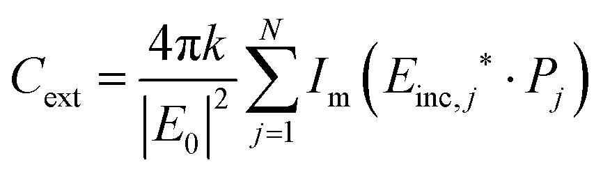
Recently, studies into SERS substrate have focused not only on a single metal particle, but also on the close-packed, well-engineered systems of metal nanostructures. Raman enhancements of 105–1010 could be obtained for molecules localized in a small volume within the interparticle interstice at an appropriate wavelength and polarization and for a small enough interparticle gap.146 For a simple dimer model, two nanoparticles can get close enough together to generate an optical field, for which the strength in the interstitial “hot spot” region can reach ∼1011 or more.147 Here, light of the appropriate wavelength is used and the exciting electric field vector is polarized along the interparticle axis, which we discussed above in Section 3.2.
The observation was made that strongly interacting metal nanoparticles result in much more effective SERS-active systems than isolated single nanoparticles and polarization sensitivity can be shown by nanoparticle aggregates.127 In addition, the enhancement relies on the size, shape, component and the surrounding medium of the nanostructures.14 Nowadays, for attempts to achieve a greater level of structural control than before, most of the assemblies consist of systems of interacting nanoparticles or hot spots based nanostructures.
 | (16) |
 | (17) |
Different parameters that can largely affect the interactions between plasmonic nanostructures and fluorophore molecules have been examined, such as the distance between the fluorophore molecule and the metal nanostructure.156–159 When the fluorphore is close to the nanostructure by a small distance, non-radiative decay dominates and the emission is quenched.160 With the distance increasing, i.e. around an intermediate distance (5 nm), in the competition between non-radiative decay and the enhancement effect, the latter begins to dominate.156 A maximum fluorescence intensity was observed when the molecule was ∼5 nm away from the surface of the Au nanosphere, which resulted from a synergic action of the excitation rate enhancement and the modification of the overall quantum yield.161 In general, the occurrence of molecular absorption-plasmon resonance coupling requires a strong overlap between the absorption and plasmon bands and a high number density of dye molecules that are positioned within ∼5 nm of the metal surface.162 For greater distances, i.e. 10 nm and above, the amplification tapers off to eventually reach unity. When distance is up to ∼30 nm, there is no overlap between the absorption and plasmon bands. It was found that the detailed model of the distance dependence of the fluorescence enhancement was beyond Lakowicz's model, and so needed to be carried out by numerical simulations using Maxwell's equations.163,164
Metal nanostructures modify the incident electromagnetic field and increase the field amplitude, especially close to sharp tips and edges as well as in tight junctions between metal nanostructures.165 The fluorophore emission intensity depends on the square of the local exciting field as well as on the fluorophore cycling rate as described by its lifetime. The plasmonic enhancement of fluorescence can be described as the coupling of fluorophores (sources of radiation) to metal nanostructures, which then act as antennas and relay the radiation outward.150,166 Based on the plasmonic nanostructure, the radiative scattering efficiency of a fluorophore can be enhanced, which is an effect related to the magnitude of its radiating dipole, and this in turn reflects the antenna size. Individual spherical metal nanoparticles that are tens of nanometres in size produce some increase in the radiating dipole that can be well described by Mie theory calculations of the radiative scattering cross-section.58,156
Through continuous investigation of fluorescence enhancement, great efforts have been devoted to constructing more complex metal nanostructures and nanoparticle assemblies.
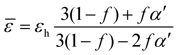
In addition, the electromagnetic enhancement of SEIRA may be calculated using effective medium theories (EMT), which are applied for the treatment of a collection of particles in a thin film. The effective medium theory, regarded as a semi-empirical approach, was developed to predict the response properties of composites, and provides a formal approach to simulate the effective dielectric function of an inhomogeneous medium, for instance, of metal–organic thin films.171 Finding the dielectric function for the surface-enhanced sample involves finding the effective optical properties of the mixture of these components. The Maxwell–Garnet and the Bruggeman methods are widely used for effective medium calculations. The general form of the Maxwell–Garnet model can be given as:172
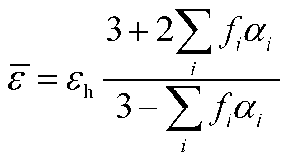 | (18) |
![[small epsilon, Greek, macron]](https://www.rsc.org/images/entities/i_char_e0c6.gif) is the effective dielectric function, and εh is the dielectric function of the host material, in which the particles are embedded, while f represents the volume fraction of the inclusions. This fundamental principle of the EMT can be utilized for calculation of the distribution of shapes and sizes of the nanoparticles.
is the effective dielectric function, and εh is the dielectric function of the host material, in which the particles are embedded, while f represents the volume fraction of the inclusions. This fundamental principle of the EMT can be utilized for calculation of the distribution of shapes and sizes of the nanoparticles.
Following, Bruggeman made a great improvement to the Maxwell–Garnet theory.173 The Bruggeman model is a self-consistent theory that includes a greater amount of interaction between inclusions.125 Commonly, the Bruggeman method is used to estimate the average “effective” optical and/or electrical parameters.174 Generally, this formalism can be expressed as:125
 | (19) |
Additionally, the chemical contribution is another consideration for SEIRA, similar to SERS, based on the charge oscillations between molecular orbitals and the increase in the absorption coefficient of absorbates.170
4. Surface-enhanced spectroscopy on nanoparticle assemblies
The self-assembly of nanoparticles as a simple, controlled and effective bottom-up method has become a very active field of research for application in the fabrication of probes, substrates and nanoparticle aggregates for SES. These theories for SERS can be included in the studies of other relevant spectroscopies in SES, like SEF, SEIRA and SEECL, through a comparison of the theories and experiments. Notably, the variety of responsive variables from SES depend on the plasmonic metallic nanostructures, as mentioned in Section 3. The strategies and applications of SES on nanoparticle assemblies are reviewed in the following.4.1 Surface-enhanced Raman spectroscopy on nanoparticle assemblies
SERS is defined as a phenomenon associated with the remarkable enhancement of the electromagnetic field near very small metal (or other) objects, which are optically excited by dipolar resonance, such as SPP or LSPP. As an effective and practical tool, SERS can produce an enormous enhancement of the Raman signal and is sensitive enough for trace detection in various fields, even low to molecular detection.The plasmonic nanostructure plays an important role in SERS applications based on a combination of nano-science and Raman spectroscopic technology. The dramatic development of nano-science and nano-technologies offers many new possibilities, notably in terms of plasmonic nanostructure design and fabrication. Among the thousands of literature reports on SERS published every year, the key issues are focused on the strategies and the applications.
The self-assembly of nanoparticles was used as a means of controlling the nanoscale building blocks for building different nanostructures. Developments in the fabrication and synthesis of noble nanostructures of controlled size, composition and shape have led to a class of well-defined nanostructures whose plasmon resonant frequencies can be manipulated through control of the geometry of the individual nanoparticles.175 As a simple, effective and low-cost method, self-assembly is established for large-scale fabrication of the nanostructure and for controlling the interparticle distance. The gap between particles is vital for plasmon coupling, giving rise to the coupling strength and resonance frequency. Also, the effect of the shape of the nanoparticle influences the coupling behaviour, which has been proved. Thus, all these parameters are taken into account for developing more efficient plasmonic regions. The plasmonic regions comprise namely the hot spots as well as the nano-tips and nano-edges. The hot spots of the coupled nanostructures lead to promising effects for surface-enhanced spectroscopy due to their strong electromagnetic field.
Nanoparticle assemblies have been explored as “tags”, which provide a unique optical “signature” for identifying them, due to their combined molecular fingerprint specificity and single-molecule sensitivity. Owing to the plasmonic nanocluster giving remarkable signal enhancements on SERS, considerable effort has been devoted to the development of probes and sensors based on nanoparticle assemblies. As it is currently understood, single-molecule surface-enhanced Raman scattering (SMSERS) is dependent on the probe containing regions of high electromagnetic field (hot spots), which can be observed in the junctions between metallic nanoparticles. Nanoparticle assemblies used for probes have attracted tremendous interests and the understanding of them has grown more and more deeply since they first appeared. Nanoprobes for SERS are those other than the substrates, which are dimerized or aggregated in the wet surroundings and which are more targeted. Most nanoprobes have been assembled by quasi-spherical or anisotropic metal nanoparticles. Generally, there are three research directions: (1) the composition, shape and structure of the constitutive nanoparticles; (2) the means of assembly; (3) controlling the interparticle distance.
Spherical nanoparticles are the most widely used for the self-assembly of nanostructures. Dimers of spherical nanoparticles are the simplest possible clusters serving as nanoprobes. In the early stage of their development, silver spheroidal nanocrystal dimers as the active structure were used in single-molecule detection.176 Nevertheless, the salt-induced self-assembly occurred on the supports, not in the solution; and so the method is more used for building the aggregates on the solid support rather than as probes. Besides, for single-molecule detection, the sensitivity of this method is usually limited by the distance between the reporter and substrate or the absence of interparticle plasmonic coupling effects. To facilitate an improvement in the sensitivity, Fabris et al. developed apta-tags as an optical reporter, formed by linking silver nanoparticles with an organic dithiol molecule, followed by surface modification with thiolated single-stranded DNA (ssDNA).59 To improve the uniformity of the constituent nanoparticles, Xia's group developed a facile method for preparing dimers of well-defined silver spheres by etching the silver nanocubes in an ethanol solvent.177 However, some limitations hamper the applications of silver nanostructures, such as their higher cytotoxicity.178 Even though, as nanoprobes, silver nanoparticles are more efficient than other noble metals (Au or Cu), these others remain the most commonly used materials for SERS cellular sensing. Gold nanospheres were chosen as the block for constructing a dimer in one study due to them giving a unique optical response and biocompatibility.179 Besides, the coupling plasmon is highly sensitive to the size and morphology of the nanoparticles.180 To better organize the process of assembling, these nanoparticles are mostly directly assembled by a biomolecule (e.g. DNA) and conjugated by chemical linkers (e.g. rigid, multivalent thiol-linkers, phenyl acetylene, thiol-terminated hydrophobic ligands and diamines).181 After dimers, a series of trimers and tetramers (e.g. pyramidal or chiral) of gold nanoparticles were designed as sensitive probes for SERS.179,182–185 Moreover, for avoiding dissociation and aggregation problems, dimers or trimers of nanoparticles can be encapsulated by polymers (e.g. PSPAA), SiO2 or another metallic shell.184,186 Note that the shells not only provide secure anchoring sites for biofunctionalization but also improve the long-term stability of the nanoparticles’ organization. Another key for nanoclusters is the interparticle spacing. Nam and co-workers developed an approach for SERS-active nanodumbbells, where the nanoscale gap between two nanoparticles could be precisely controlled.187 The EM coupling in a dimer or larger assemblies results in a huge EM field enhancement at the nanogap. For example, the interparticle distance within nanoparticles is precisely tailored in the order of a few nanometres with changing the molecule length of the DNA bridge.54 Lan et al. reported that the E-field EF increased from 7.8 to 23.4 as the interparticle distance decreased from 15 nm to 5 nm; on the other hand, the size increases with the E-field EF increasing.54 Further, significantly increases in the EM field were observed as the interparticle distance decreased from 1 to 0.5 to 0.25 nm.188 Therefore, the interparticle spacing within nanoparticle assemblies is a crucial factor for plasmonic coupling.
According to the LSPR theories, the optical properties of nanoparticle assemblies are strongly dependent on their geometry.189,190 Larger number of spheres aggregating represents the next level of complexity beyond dimers. Among these, tetrahedral (pyramidal and chiral) nanoparticle assemblies have been organized by DNA with a well-controlled geometry185,191,192 (Fig. 12). Using the pyramidal assemblies, three disease biomarkers could simultaneously be detected at the atto-molar level.
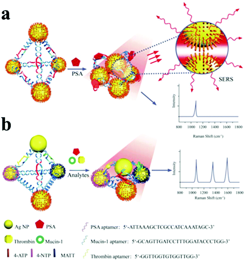 | ||
| Fig. 12 Scheme of Ag pyramids self-assembled by DNA frame for SERS analysis of biomarkers. (a) Ag nanoparticles were modified with 4-ATP, PSA aptamers were inserted in each side of DNA frame of pyramid structure. (b) Three Ag NPs in each pyramid were modified with 4-ATP, NTP, and MATT, respectively, and three aptamers were inserted in three sides of the DNA frame of pyramid structure, respectively. (Reprinted from ref. 192; Copyright 2015, John Wiley and Sons.) | ||
Besides, plasmonic core–satellite structures, which result in coupled plasmonic assemblies, are of high interest in surface-enhanced vibrational spectroscopy. For example, a core–satellite nanocluster comprised of shape-controlled plasmonic nanostructures can be achieved through self-assembly using simple molecular cross-linkers.53 The number of satellites around the cores can be controlled by varying the volume of the satellite solution added to the core solution. Li et al. developed an approach where three kinds of hairpin DNA species (denoted as H1, H2 and H3, respectively) were used to immobilize gold nanoparticles193 (Fig. 13). Therefore, the in-built electromagnetic hot spots and Raman reporters of core–satellite structures make them excellent candidates for surface-enhanced Raman scattering probes.
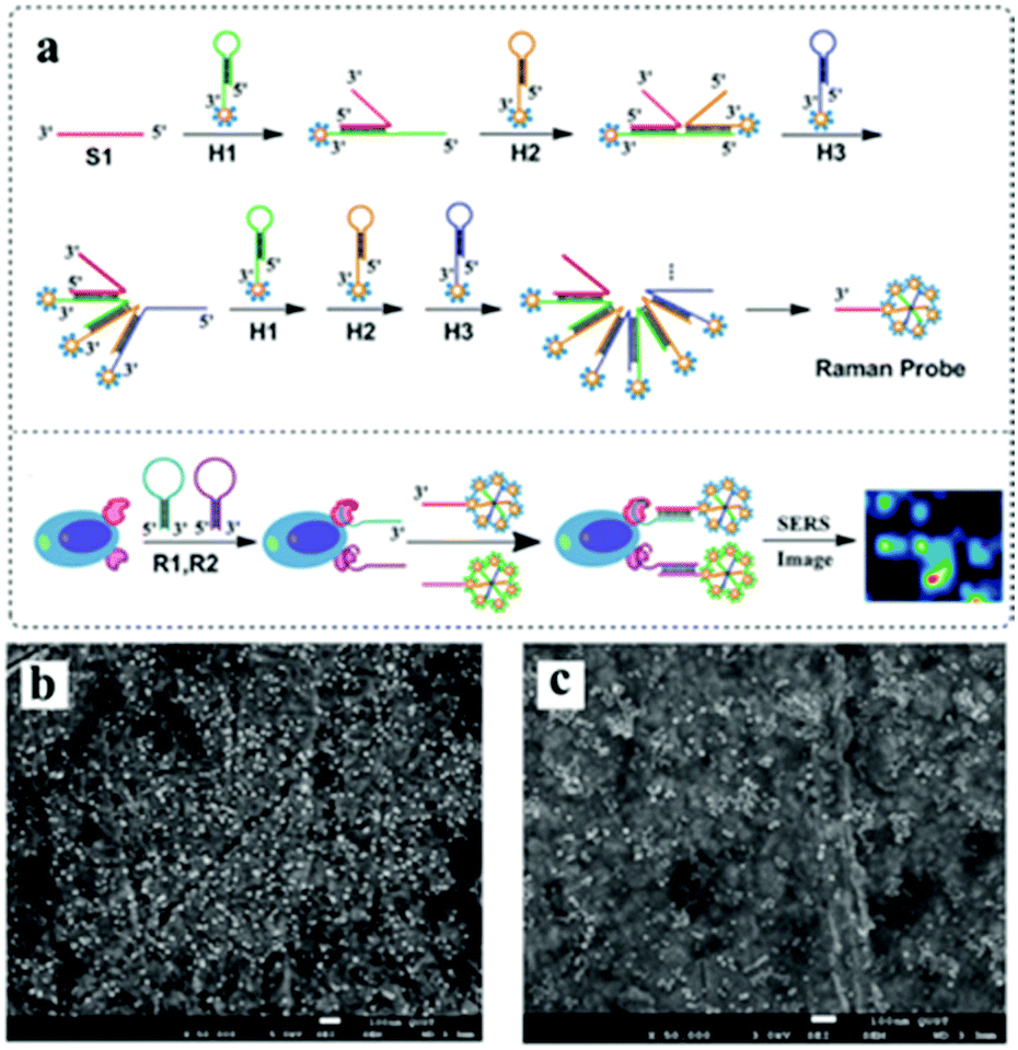 | ||
| Fig. 13 (a) Schematic for the self-assembly of branched DNA–gold nanoaggregates. (b) SEM images of the prepared AuNPs. (c) SEM images of the fabricated DNA–gold nanoaggregates after mixing the linker DNA (S1) and three kinds of hairpin DNA-barcode–Au nanoprobes for 1 h at 20 °C. (Reprinted from ref. 193; Copyright 2014, Royal Society of Chemistry.) | ||
Gold nanorods are one of the most typical particles with an anisotropic shape, which can undergo different forms of assembly.175 Because of the anisotropic shape, nanorods can be assemblies into end-to-end or side-by-side structures and can be derived from L-shape and T-shape modes via different modifications of the nanorod surface194–196 (Fig. 14). Plasmonic dimeric nanostructures can be precisely tuned with the orientation of nanorods, and exhibit a well-defined mutual alignment and EM field changes located in the junction section.195 Similarly, the assembly of nanorods can be performed using chemical methods and biomolecule linkers, and they are usually encapsulated with a “shell” to maintain the stability.187,197,198 A larger enhancement in the signal intensity was observed from the end-to-end form of dimers rather than from the isolated Au nanorods, which is due to the enhancement of the electric field at the junctions199 (Fig. 14). Besides, to further control the process of dimerization, the sides or ends are usually encapsulated by polymers with exposed parts that can be modified or linked.198,200 However, in contrast to the end-to-end form, side-by-side assembled nanorods were demonstrated to not be suitable for use as highly sensitive SERS probes (Fig. 15).200 Extending to larger numbers, Lee et al. reported that the chains of nanorods could be assembled in an end-to-end manner, which provided a direct correlation between ensemble-averaged surface-enhanced Raman scattering and the extinction properties of the chains, as a function of the average aggregation number of nanorod chains during their assembly.201 Therefore, gold nanorods are well suited for the fundamental studies of the optical properties of aggregated nanoparticle systems and for use as nanoprobes in solution.
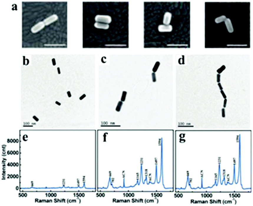 | ||
| Fig. 14 (a) SEM images of two rods aligned end-to-end, side-to-side, in a T configuration, and in an L configuration. All scale bar, 100 nm. (Reprinted from ref. 195; Copyright 2009, American Chemical Society.) (b) TEM images of gold nanorods (b–d) and Raman spectrum of bipy-DT (e–g) at various stages of plasmon coupling; incubation (b and f), dimerization (c and f) and oligomerization (d and g) steps. (Reprinted from ref. 199; Copyright 2011, American Chemical Society.) | ||
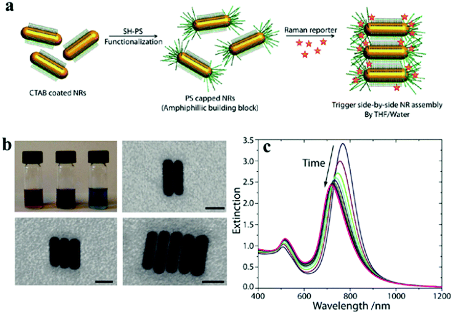 | ||
| Fig. 15 The self-assembly of gold nanorods used for SERS tags in a side-by-side way. (a) Schematic illustration of the side-by-side NR assembly. A SH-PS is attached to the ends of CTAB-coated gold NRs in THF via site-specific ligand exchange. After the addition of the Raman reporter, the side-by-side assembly was triggered by the addition of water (10 vol%). (b) Photograph showing a typical change in colour of the solution of self-assembling NRs as a function of time from reddish-purple to blue (top left). Representative scanning transmission electron microscopy images of NRs in various stages of self-assembly. The scale bar is 15 nm. (c) Variation in extinction properties of NR ensembles over time. (Reprinted from ref. 200; Copyright 2012, American Chemical Society.) | ||
These nanoparticles, like nanorods, nanoplates, nanocubes, nano-polyhedrons, nanoflowers and nanostars, are also used for dimeric assemblies with the junction region of nano-corners, nano-tips or nano-edges, which can provide stronger Raman scattering intensities than their rounded counterparts as they allow for a higher concentration of near field.14,134,202 Ma et al. developed a method to synthesize a dimer of nanostars as a SERS-probe based on the Hg2+-mediated T–T base pair of ssDNA.203 Song et al. reported a benzoic group functionalized gold nanoflower as a bridge probe for both the recognition of target sialic acids and for the assembly of poly(N-acetylneuraminic acid) modified gold nanoparticles204 (Fig. 16). The special core–satellite structure led to plasmonic coupling of two kinds of gold nanoprobes, which produced a sensitive SERS signal for the imaging of sialic acids in living cells. Multiple nanoprobes can be assembled together and offer the potential of simultaneous SERS detection.
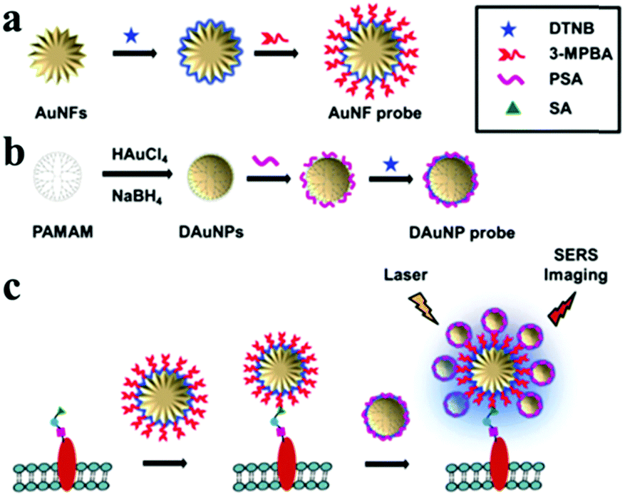 | ||
| Fig. 16 Core–satellites self-assembly of gold nanoflowers and gold nanospheres. Schematic illustration of: (a) preparation of the AuNF probe, (b) preparation of the DAuNP probe, and (c) SERS imaging of the cell surface SAs based on plasmonic coupling of the core AuNF with the satellite AuNPs. 3-MPBA represents 3-mercaptophenylboronic acid. (Reprinted from ref. 204; Copyright 2016, Royal Society of Chemistry.) | ||
Assembling colloidal nanoparticles into the dimer structure can be achieved by fine tuning the colloidal stability. Salt, like sodium chloride-induced nanoparticle aggregates were not controlled by centrifugation or by changing the dispersion medium or the ionic strength.208–212 Xia et al. reported a simple and one-step method that generated dimers without any additional assembly steps, but which depended on the control of the colloidal stability and oxidative etching by optimizing the amount of chloride added to a polyol synthesis.211 The formation of dimers was achieved due to the change in the colloidal stability. However, the salt-induced method is poor at controlling the number of constitutive nanoparticles and the ordering arrangement.
Besides, nanocluster arrays are designed by manipulating some parameters, such as the average interparticle separation of the nanoparticles within the clusters and the separation between the clusters, resulting in field enhancements. To better achieve an ordered arrangement, self-assembly and other techniques are extensively combined to build nanocluster arrays. Template-guided self-assembly methods are used for designs that organize particles on a pattern of binding sites.65 Using a large-area/low-cost nanopatterning method in conjunction with a meniscus force deposition technique, Alexander and co-workers were able to create large arrays of uniformly spaced nanoclusters comprising two 60 nm gold nanospheres.213 The ordered arrays of dimers could be tuned by the size, orientation and placement with respect to the fiducial patterns.
The spin-coating assisted self-assembly of cluster arrays has attracted plenty of attention, because it is an efficient and low-cost method without any expensive equipment. Based on the methods, the coated platform has a wide variety of options, not confined to just a flat support.214 There are two ways of spin-coating: first, the core nanoparticle is spin-coated on the chip as the “anchor”, followed by the self-assembly of other nanoparticles to form the structure of the “core–satellite”;43 second, the pre-assembled nanoclusters can be directly spin-coated onto the support.215 Besides, Zheng et al. reported a simple approach without using nano-lithographic methods. The gold core–satellite nanostructures could be obtained using electrostatic and DNA-directed self-assembly121 (Fig. 17).
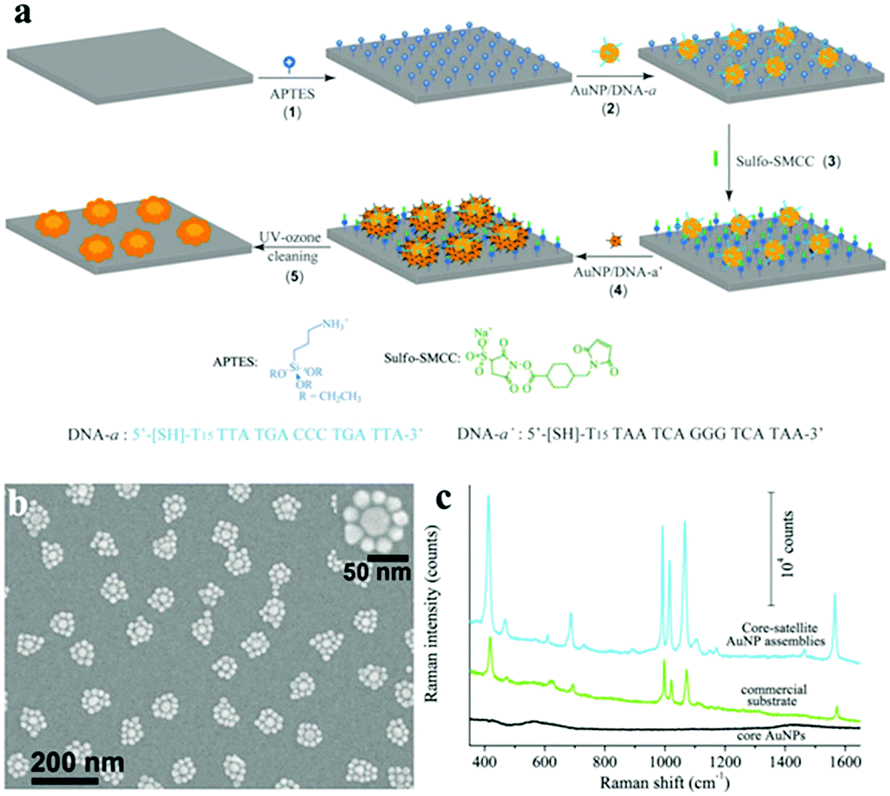 | ||
| Fig. 17 (a) Scheme of the hierarchical self-assembly procedure for the fabrication of core–satellite plasmonic nanostructures. (1) APTES functionalization of a glass substrate. (2) Electrostatic immobilization of 30 nm AuNP–DNA conjugates onto the APTES-modified substrate surface. (3) Neutralization of surface-confined amino groups by the formation of covalent amide bonds with sulfo-SMCC; (4) hybridization of 20 nm AuNP–DNA conjugates onto the 30 nm AuNPs, forming the core–satellite nanoparticle assemblies. (5) Removal of the surface-confined molecules through UV-ozone cleaning, yielding pristine gold surfaces. (b) SEM images of an array of core–satellite nanostructures on a silicon substrate obtained by immobilization of 20 nm satellite AuNPs onto the core-AuNPs. (c) SERS spectra of benzenethiol adsorbed on the core–satellite AuNP assemblies (blue line), a commercial Klarite SERS substrate (green line) and 30 nm core-AuNPs only (black line), excited at 782 nm. (Reprinted from ref. 121; Copyright 2013, John Wiley and Sons.) | ||
Generally, monolayer nanoparticle arrays were originally prepared by depositing nanocrystal suspensions on substrates (such as carbon-coated copper grids or silicon wafers), followed by evaporating the solvents.91 However, it has been found that both the evaporation kinetics and the amount of excess capping ligands affect the formation of the monolayer at the liquid–air interface.63 As observed, multiple factors impact the droplet-evaporation method, which results in different forms, like the “coffee-ring”, 2D monolayer film or 3D superlattice.216 Based on the coffee-ring effect, Wang et al. developed an efficient SERS platform, which integrated the self-assembly of silver nanospheres and the preconcentration of analytes into one step.44 Furthermore, spherical multitip gold mesoparticles are capable of self-assembling into monolayer or multiple layer arrays on Si substrates following a simple droplet-evaporation deposition.217 As the key factors of close-packed nanoparticle monolayers, the shape, size and periodicity (for arrays) of the metal features explicitly determine the profile and intensity of the observed optical response.75 Lin and co-workers reported a simple and efficient method for fabricating large-area (>1 cm2) 3D gold or silver films218 (Fig. 18). In this method, the close-packed monolayers used a layer-by-layer assembly from suspensions of thiolate-passivated gold or silver colloids. Chen and co-workers presented a large-area (over 1 mm2) hexagonal close-packed structure of alkanethiol-stabilized gold nanoparticles.219 The interparticle spacings were finely tuned from 2.3 to 3.4 nm by controlling the alkyl chain lengths of the alkanethiols from 12 to 18 carbon atoms. On the other hand, stabilizing surfactants play an important role in the formation of ordered nanostructures.
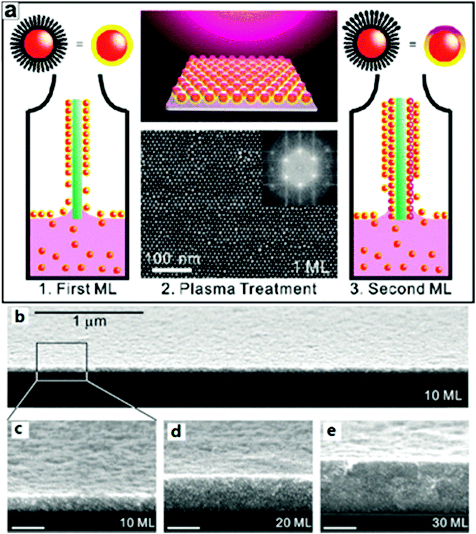 | ||
| Fig. 18 (a) Schematic illustration of the plasma-assisted LbL assembly process. (b) FE-SEM micrographs of AuNP supercrystal films. (b) Large-area and (c) high-resolution cross-sectional SEM micrographs of a 10 mL AuNP film deposited on a Si substrate (imaged on the cleaved face). (d and e) Cross-sectional SEM micrographs of 20 and 30 mL AuNP films deposited on Si substrates. (Reprinted from ref. 218; Copyright 2010, American Chemical Society.) | ||
While other nanoparticle monolayer films over large areas can be prepared through various approaches, a major challenge is to reproducibly prepare stable enhanced substrates with uniform hot spots and possibly to push the gaps to the sub-nanometre regime in order to enhance the sensitivity. The droplet-evaporation technique has also been employed to produce ordered assemblies of Au nanostructures with other shapes, including polyhedra, nanocubes and bipyramids.92 A ring with ordered assemblies of Au nanostructures is left on the substrate in these cases. However, inside the ring are disordered nanostructure assemblies, which are a few layers in thickness. Droplet-evaporation allows the fabrication of crystallites limited to the micrometre range, while achieving only local order due to the coffee-ring effects. Liz-Marzán and co-workers reported the synthesis of high-quality nanotriangles, followed by assembling at the air–liquid interface to obtain nanotriangle monolayers220 (Fig. 19). The possibility of fabricating homogeneous substrates over large areas is most relevant, especially when compared with methods such as droplet-evaporation. Using self-assembly at the oil–water interface, Wang's group reported a series of superstructure assemblies, including monolayer and multilayers, by tuning the ratio of hydrophilic/hydrophobic molecules added and the chain lengths.55,221
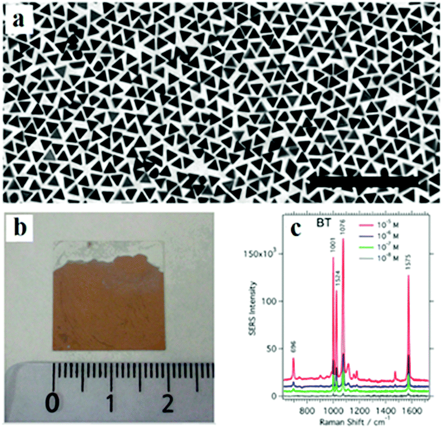 | ||
| Fig. 19 (a) TEM images of gold nanotriangles (Au NTs). (b) Optical photograph of the Au NT@PVP monolayer on a glass slide. (c) SERS spectra of thiolsbenzenethiol excited at 785 nm with concentrations varying between 10−5 and 10−8 M. (Reprinted from ref. 220; Copyright 2014, American Chemical Society.) | ||
The anisotropy of gold nanorods renders the vertical arrays with a strong nanoantenna effect. Peng et al. reported an evaporation-induced vertically aligned monolayer with a nominal 0.8 nm gap distance, which exhibited high sensitivity.72 The nanorods could be assembled together in a side-by-side fashion to form layers and the layers were then packed nearly parallel to each other into a 3D structure.92
Silane-ligand-modified surfaces can be used for fabricating monolayer substrates by an electrostatic self-assembly. Su et al. performed a gold nanostar layer onto an ITO glass slip, which was prepared by a low-cost electrostatically-assisted APTES-functionalized surface-assembly method for SERS analysis.222 It was found that the substrate assembled by the nanostars with the longest branches generated the biggest enhancement when other experimental conditions (such as the laser frequency and power) were controlled to be the same.
Typically, the droplet-evaporation method is widely used to fabricate multilayer assemblies. The size and shape are important for the formation of ordered superlattices.224 In particular, the shape of the nanoparticles determines the structure and morphology of the superlattices during the assembling of the monodispersed nanoparticles.37
To obtain a huge electric field concentration of crystalline structure with intense and controlled antenna effects, Liz-Marzán and co-workers developed superlattices of standing core–shell gold–silver nanorods stabilized by gemini surfactants. Notably, gemini surfactants comprising two hydrophobic tails and two hydrophilic headgroups linked by a molecular spacer have been proven to be excellent stabilizers and binders in nanoparticle synthesis and self-assembly225 (Fig. 20).
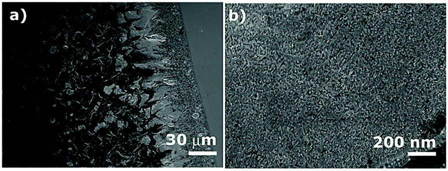 | ||
| Fig. 20 (a) SEM images of the coffee-ring deposits. (b) Enlarged view of SEM images showing standing 3D superstructures (ring width ∼30 μm). (Reprinted from ref. 225; Copyright 2013, John Wiley and Sons.) | ||
Even though evaporation-induced nanoparticle assembly on solid surface is widely used, the coffee-ring effect cannot be neglected,44,216,224 and results in ordered nanostructures usually observed at a relatively small area close to the ring edge. Moreover, utilizing confined geometries can achieve evaporative self-assembly in special geometries.226 Thus, long-range-ordered self-assembly is a still challenge, due to the strong interaction force and low diffusion rate. To overcome this limitation, some strategies for suppressing the coffee-ring effect have been developed via the use of additives and ellipsoidal particles.227,228 Solvent evaporation-induced interfacial self-assembly was used for avoiding the coffee-ring effects at the solid substrate, which could help minimize the interfacial energy and improve the convection velocity.229–232 Typically, Wang's group developed a dynamically regulated strategy to achieve highly uniform, long-range-ordered Ag nanowire (Ag NW) arrays in a short time. Additionally, the oriented Ag NW arrays were applied for the SERS monitoring of a cell's adhesion and growth233 (Fig. 21).
 | ||
| Fig. 21 (a) Schematic diagram of the selective self-assembly of AgNWs on the liquid surface of chloroform: (i) the flow of mixed solutions, (iia) the nanowires’ selective arrangement, and (iib) large numbers of nanoparticles assembled on the wall. Numbered images: (1) proposed model for the selective self-assembly of nanowires; (2) proposed model for the assembly of nanoparticles on the wall with the decrease of the liquid surface. (b) Typical SEM image of the selective self-assembly of AgNWs at the water–air interface corresponding to model 1 in (a). (c) Typical SEM image of the assembly of AgNPs on the vessel wall corresponding to model 2 in (a). (d) Schematic illustration of cell adhesion and growth on (ia) oriented AgNW arrays and (iia) random AgNW films. (e) Typical Raman spectra of the cells cultured for 1, 2 and 6 h on the oriented AgNW arrays. (f and g) Typical SEM images of the cells cultured for 12 h: (f) on the oriented AgNW arrays and (g) on the random AgNW films. (Scale bars: (b and c) 250 nm and (f and g) 50 μm.) (Reprinted from ref. 233; Copyright 2016, John Wiley and Sons.) | ||
4.2 Surface-enhanced fluorescence on nanoparticle assemblies
SEF is another hot research field in SES. SEF is also referred to as metal-enhanced fluorescence (MEF) and plasmon-enhanced fluorescence (PEF).234 By analogy with SERS, many plasmonic nanostructures are designed and fabricated for enhancing fluorescence. However, the direct fabrication of dimers or other aggregates in solution are occasionally used for SEF, due to the influence of the separate distance between the plasmon and the fluorophore.163 Therefore, utilizing core–shell nanostructures to separate the plasmon and the fluorophore is one of the main strategies used in SEF. Additionally, regular arrays of metallic nanostructures were observed with strong electric fields (hot spots) at the gap between two neighbouring nanostructures with intensified LSPR. Among these strategies, the combination of a core–shell nanostructure and nano-array has attracted considerable attention.In the past years, various types of metal nanostructures, consisting of special spacer layers, with different shapes and metallic species, have been used for fabricating effective SEF-active nano-arrays.235 The metallic species used for the fabrication of SEF-responsive plasmonic nanostructures are not only limited to Au and Ag, but also include Cu and Al.163,236–238 Among these, Ag and Au have attracted most attention. The effects of metal nanoparticles for enhancing the luminescence of CdSe quantum dots have been compared, by Batteas's group.239 They developed a single layer of quantum dots on top of arrays of the desired metal nanostructure positioned in a grid pattern, in which the separation between the two was controlled with a polymer spacer formed using layer-by-layer assembly. By changing the thickness of the polymer spacer, the photoluminescence enhancement of CdSe was found to peak at a factor of 2 at distances of ∼11 and 8 nm, when coupled to Au and Ag particles respectively (Fig. 22).
 | ||
| Fig. 22 (a) Confocal scanning microscopy image generated by collecting the 488 nm laser line on nine layers of polymers deposited upon Au-NP patterned GaAs surfaces (the z-scale bar is from 50–850 a.u.). (b) Spectra on the GaAs background (red circle) and Au-NP patterned (white circle) regions. The red line and the black line represent the averaged spectra of the reflected laser light of red circle and white circle areas in panel A, respectively. (c) The corresponding confocal image at the same scanning region generated by collecting the 488 nm laser line on five layers of polymers deposited upon Ag-NP patterned GaAs surfaces. (d) Reflected laser light from the GaAs background (green circle) and the Ag-NP patterned (white circle) regions. The green line and the black line represent the averaged spectra of green circle and white circle areas in panel C, respectively. (e) Schematic cross-sectional view of the sample showing that polymers and 4 nm QDs were deposited onto Au-NP arrays on GaAs in sequence. (Reprinted from ref. 239; Copyright 2009, American Chemical Society.) | ||
For the assembly of nano-arrays, common nanostructures, such as nanospheres, nanorods, nanotriangles and nanocages, have been used.238–240 Nanospheres are the most widely used for fabricating ordered arrays and close-packed sheets, due to their high controllability and symmetrical structure.241 Beyond that, the self-assembly of anisotropic nanostructures was used to fabricate a plasmonic surface of an ordered array. Au NR is a promising anisotropic nanostructure for direct assembly in an ordered array format on a substrate. Mei and co-workers developed a SEF-based DNA detecting platform where fluorescence-labelled hairpin ssDNA was modified on an ordered array of vertical Au NRs for capturing the complementary ssDNA.240 By varying the number of base pairs in the DNA duplex, the fluorescence intensity could be tuned. Furthermore, the exposing tips in the vertical arrays could amplify the SPR signals at neighbouring particles collectively. As such, the nanostructures of nano-tips and nano-corners were demonstrated to be able to generate a significant local enhancement of the surrounding EM field. Xia's group developed Au nanocage arrays as an enhancing substrate through microcontact printing and investigated the potential of the Au nanocages as a novel class of MEF substrates in the NIR region.242 MEF was demonstrated with NIR light-emitting films and electrospun polymer nanofibres, with additional spatial control provided by microprinting of the nanocages.
It is well known that MEF critically depends on the distance between the metal surface and the fluorophores. Thus, the design of the spacer layer is commonly used in MEF substrates. For arrays, there two main ways for fabricating the spacer layer: one is by building a pre-coating shell of the nanostructures before assembling, and the other one is coating, spinning and growing a layer finely, or modifying a molecular layer on the assembled nanostructures.240,242 The common materials for the spacer layer involve polymer materials, semiconductor nanomaterials and DNA molecules.
4.3 Other surface-enhanced spectroscopies on nanoparticle assemblies
Surface-enhanced infrared absorption (SEIRA) is another important surface-enhanced vibrational spectroscopy, besides SERS.128 However, SEIRA has received much less attention than SERS. Generally, SEIRA and SERS complement each other. Similar to SERS, two different mechanisms, namely an electromagnetic effect and chemical effect, are supposed to contribute to the total SEIRA enhancement (refer to Section 3.4.3). SEIRA can also provide several orders of magnitude enhancement in the IR region. Numerous metallic substrates, such as roughened or metal island films, fabricated arrays of small metallic antennas, where molecules are located on or near the structure, are created to provide a sufficiently strong signal for SEIRA detection.243,244 The self-assembly of nanostructures has been developed for fabricating plasmonic SEIRA substrates, due to the low cost and high throughput.245 For example, Halas and co-workers focused on the application of nanoshells for SEIRA.246,247 By the droplet-evaporation method, gold nanoshells were assembled into periodic arrays with nanoscale interparticle gaps, which could provide significant enhancements to both SERS and SEIRA, effectively combining both spectroscopies on a single substrate. Simultaneously, molecular detection and characterization could be achieved with high precision and sensitivity, through SERS and SEIRA. Notably, the sub-10 nm interparticle gaps between the nanostructures can induce strong plasmon coupling, which results in the specific electromagnetic properties of this array geometry (Fig. 23). | ||
| Fig. 23 (a) Fabrication of Au nanoshell arrays. (b and c) SEM images of nanoshell arrays formed by drying 40 μL of aqueous solutions of CTAB-capped Au nanoshells on silicon wafers. The core radius of the nanoshells is 150 ± 12 nm, and the shell thickness is 22 ± 1 nm. (d) TEM image of the nanoshell arrays formed on a TEM grid. (e) Empirical SERS enhancement factors of para-mercaptoaniline (pMA) adsorbed on nanoshell arrays and the isolated nanoshells. (f) Normal IR spectrum of pure pMA and the SEIRA spectrum of pMA SAMs on the nanoshell arrays. (Reprinted from ref. 246; Copyright 2007, John Wiley and Sons.) | ||
Surface-enhanced electrochemiluminescence (SEECL) is one of the fastest developing methods in the surface-enhanced spectroscopy family. Similar to SEF, SEECL was found to be strongly dependent on the distance between ECL emitters and the plasmonic nanostructures, due to the competition between field enhancement and Förster resonance energy transfer (FRET).31 Generally, ECL emitters and plasmonic nanostructures are assembled on the surface of solid electrode in SEECL. The ECL intensity can be altered by controlling the thickness of the silica shell or length of the DNA30,31,248 (Fig. 24). Wang et al. positioned Au NP@SiO2 on a modified gold electrode though electrostatic self-assembly.29 They demonstrated that the LSPR-field enhancement of ECL is the dominant factor when the shell thickness increases from 2 nm to 6 nm. Even though some studies have been reported, SEECL is still a young subject in SES.
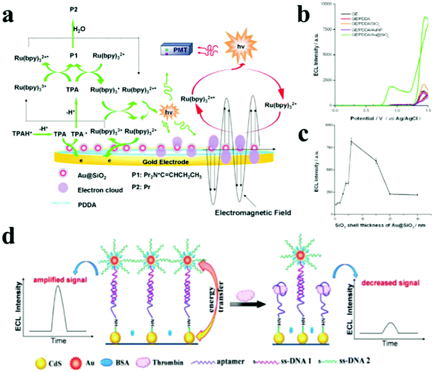 | ||
| Fig. 24 (a) Schematic of SEECL of the AuNP@SiO2-modified electrode. (b) ECL emission of GE (blank), GE/PDDA (red), GE/PDDA/SiO2 (orange), GE/PDDA/AuNPs (violet) and GE/PDDA/AuNP@SiO2 (green, the thickness of the silica shell is 4 nm). (c) Relationship between ECL intensity of AuNP@SiO2-modified electrodes and the silica shell thickness. Error bars represent the standard deviations of 5 replicates; (Reprinted from ref. 29, 2015, Springer Nature) (d) ECL Aptamer sensing platform based on energy transfer between CdS NCs and Au NPs. (Reprinted from ref. 31; Copyright 2011, American Chemical Society.) | ||
5. Summary and perspectives
In summary, in recent years, a lot of efforts have been paid to the fabrication of different kinds of ordered nanoparticles, and the potential applications of these nanostructures for SES have been investigated in detail (Fig. 25). As stated in the text, a number of mechanisms and properties behind these phenomena have been proposed. These efforts have greatly improved the development of SES. Nevertheless, the trends in the near future in nanoparticle assemblies should still focus on the fabrication of new supercrystals with superior properties compared to individual nanoparticles. The following two ways are the most likely to realize such a purpose: first, a diverse strategy to develop multi-functionalities of supercrystals, which could generate interparticle optical, electric or magnetic elements communications; second, the fabrication of nanoparticle supercrystals that consist of binary cooperative complementary materials.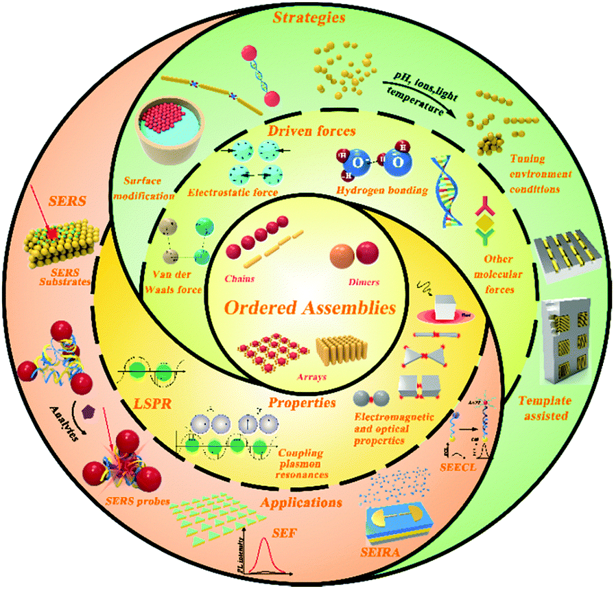 | ||
| Fig. 25 Summary of the mechanisms of ordered nanoparticle assemblies and the strategies and applications of ordered assemblies for SES. | ||
On the other hand, some issues must be solved to push these promising techniques into real applications: most of all, the mechanism of SES is still unclear and needs to be determined. Although a couple of mechanisms have been proposed to explain the phenomenon of SERS, hitherto none of these mechanisms can explain all the SERS phenomena. In addition, most of the other SES (e.g. SEIRA and SEF) cited the mechanism of SERS; however, little attention has been paid to explain the reason why the signal enhancement factor between different kinds of SES are much different even when using the same substrate; second, although a large number of approaches have been reported for the fabrication of different kinds of SES substrates, most of these substrates have been used in individual laboratories, while few of them have been commercialized. Therefore, the fabrication of economic, repeatable and universal SES substrates is still a tough task.
Conflicts of interest
There are no conflicts to declare.Acknowledgements
T. W. acknowledges the support from the 1000 Young Talents program, the National Natural Science Foundation of China (Grant No. 21635002, 21621062) and ICCAS. L. G. and Y. L. acknowledge the support from the National Natural Science Foundation of China (Grant No. 21675028, 21575027 and 21775026).References
- Y. Li, J. Zhang, S. Zhu, H. Dong, F. Jia, Z. Wang, Z. Sun, L. Zhang, Y. Li and H. Li, Adv. Mater., 2009, 21, 4731–4734 CAS.
- Z. Xie, K. Cao, Y. Zhao, L. Bai, H. Gu, H. Xu and Z. Z. Gu, Adv. Mater., 2014, 26, 2413–2418 CrossRef CAS PubMed.
- K. Liu and L. Jiang, Nano Today, 2011, 6, 155–175 CrossRef CAS.
- C. S. Zuker, Science, 1994, 265, 742–744 CAS.
- X. Gao, X. Yan, X. Yao, L. Xu, K. Zhang, J. Zhang, B. Yang and L. Jiang, Adv. Mater., 2007, 19, 2213–2217 CrossRef CAS.
- J. Huang, X. Wang and Z. L. Wang, Nano Lett., 2006, 6, 2325–2331 CrossRef CAS PubMed.
- R. A. Potyrailo, H. Ghiradella, A. Vertiatchikh, K. Dovidenko, J. R. Cournoyer and E. Olson, Nat. Photonics, 2007, 1, 123–128 CrossRef CAS.
- W. Peng, S. Zhu, W. Wang, W. Zhang, J. Gu, X. Hu, D. Zhang and Z. Chen, Adv. Funct. Mater., 2012, 22, 2072–2080 CrossRef CAS.
- J. Zi, X. Yu, Y. Li, X. Hu, C. Xu, X. Wang, X. Liu and R. Fu, Proc. Natl. Acad. Sci. U. S. A., 2003, 100, 12576–12578 CrossRef CAS PubMed.
- D. Spitzer, T. Cottineau, N. Piazzon, S. Josset, F. Schnell, S. N. Pronkin, E. R. Savinova and V. Keller, Angew. Chem., Int. Ed., 2012, 51, 5334–5338 CrossRef CAS PubMed.
- J. Krieger, E. Große-Wilde, T. Gohl and H. Breer, Eur. J. Neurosci., 2005, 21, 2167–2176 CrossRef PubMed.
- R. V. Nair and R. Vijaya, Prog. Quantum Electron., 2010, 34, 89–134 CrossRef CAS.
- F. Liu, B. Dong and X. Liu, Optical Devices in Communication and Computation, InTech, 2012 Search PubMed.
- K. L. Kelly, E. Coronado, L. L. Zhao and G. C. Schatz, J. Phys. Chem. B, 2003, 107, 668–677 CrossRef CAS.
- M. E. Stewart, C. R. Anderton, L. B. Thompson, J. Maria, S. K. Gray, J. A. Rogers and R. G. Nuzzo, Chem. Rev., 2008, 108, 494–521 CrossRef CAS PubMed.
- J. N. Anker, W. P. Hall, O. Lyandres, N. C. Shah, J. Zhao and R. P. Van Duyne, Nat. Mater., 2008, 7, 442 CrossRef CAS PubMed.
- M. Fleischmann and P. Hendra, Chem. Phys. Lett., 1974, 26, 123 CrossRef.
- C. B. Milojevich, D. W. Silverstein, L. Jensen and J. P. Camden, J. Am. Chem. Soc., 2011, 133, 14590–14592 CrossRef CAS PubMed.
- J. Kneipp, H. Kneipp and K. Kneipp, Proc. Natl. Acad. Sci. U. S. A., 2006, 103, 17149–17153 CrossRef CAS PubMed.
- A. R. Guerrero and R. F. Aroca, Angew. Chem., Int. Ed., 2011, 50, 665–668 CrossRef CAS PubMed.
- M. D. Furtaw, D. L. Steffens, T. M. Urlacher and J. P. Anderson, Anal. Chem., 2013, 85, 7102–7108 CrossRef CAS PubMed.
- G. F. Walsh and L. Dal Negro, Nano Lett., 2013, 13, 3111–3117 CrossRef CAS PubMed.
- Y. Shen, Nature, 1989, 337, 519 CrossRef CAS.
- F. M. Geiger, Annu. Rev. Phys. Chem., 2009, 60, 61–83 CrossRef CAS PubMed.
- J. Kozuch, C. Steinem, P. Hildebrandt and D. Millo, Angew. Chem., Int. Ed., 2012, 51, 8114–8117 CrossRef CAS PubMed.
- L. V. Brown, K. Zhao, N. King, H. Sobhani, P. Nordlander and N. J. Halas, J. Am. Chem. Soc., 2013, 135, 3688–3695 CrossRef CAS PubMed.
- R. Bukasov and J. S. Shumaker-Parry, Anal. Chem., 2009, 81, 4531–4535 CrossRef CAS PubMed.
- D. Wang, L. Guo, R. Huang, B. Qiu, Z. Lin and G. Chen, Electrochim. Acta, 2014, 150, 123–128 CrossRef CAS.
- D. Wang, L. Guo, R. Huang, B. Qiu, Z. Lin and G. Chen, Sci. Rep., 2015, 5, 7954 CrossRef CAS PubMed.
- D. Wang, Y. Li, Z. Lin, B. Qiu and L. Guo, Anal. Chem., 2015, 87, 5966–5972 CrossRef CAS PubMed.
- J. Wang, Y. Shan, W.-W. Zhao, J.-J. Xu and H.-Y. Chen, Anal. Chem., 2011, 83, 4004–4011 CrossRef CAS PubMed.
- Y. Shan, J.-J. Xu and H.-Y. Chen, Chem. Commun., 2009, 905–907 RSC.
- R. Yang, Y. Liu, H. Ye, B. Qiu, Z. Lin and L. Guo, Electroanalysis, 2016, 28, 1783–1786 CrossRef CAS.
- K. J. Bishop, C. E. Wilmer, S. Soh and B. A. Grzybowski, Small, 2009, 5, 1600–1630 CrossRef CAS PubMed.
- M. A. Boles, M. Engel and D. V. Talapin, Chem. Rev., 2016, 116, 11220–11289 CrossRef CAS PubMed.
- Y. Yin and A. P. Alivisatos, Nature, 2005, 437, 664–670 CrossRef CAS PubMed.
- Z. Zhu, H. Meng, W. Liu, X. Liu, J. Gong, X. Qiu, L. Jiang, D. Wang and Z. Tang, Angew. Chem., Int. Ed., 2011, 123, 1631–1634 CrossRef.
- D. Luo, C. Yan and T. Wang, Small, 2015, 11, 5984–6008 CrossRef CAS PubMed.
- D. Ben-Avraham, J. Stat. Phys., 2006, 123, 709–710 CrossRef.
- H. Hamaker, Physica, 1937, 4, 1058–1072 CrossRef CAS.
- E. Lifshitz, Perspectives in Theoretical Physics: The Collected Papers of E. M. Lifshitz, 1956, pp. 73–83 Search PubMed.
- D. Langbein, Phys. Rev. B: Solid State, 1970, 2, 3371 CrossRef.
- C. Zhu, G. Meng, Q. Huang and Z. Huang, J. Hazard. Mater., 2012, 211, 389–395 CrossRef PubMed.
- W. Wang, Y. Yin, Z. Tan and J. Liu, Nanoscale, 2014, 6, 9588–9593 RSC.
- M. Corricelli, N. Depalo, E. Fanizza, D. Altamura, C. Giannini, D. Siliqi, R. Di Mundo, F. Palumbo, V. G. Kravets and A. N. Grigorenko, J. Phys. Chem. C, 2014, 118, 7579–7590 CAS.
- E. V. Shevchenko, D. V. Talapin, C. B. Murray and S. O'Brien, J. Am. Chem. Soc., 2006, 128, 3620–3637 CrossRef CAS PubMed.
- H.-J. Yang, S.-Y. He, H.-L. Chen and H.-Y. Tuan, Chem. Mater., 2014, 26, 1785–1793 CrossRef CAS.
- P. M. Claesson, T. Ederth, V. Bergeron and M. Rutland, Adv. Colloid Interface Sci., 1996, 67, 119–183 CrossRef CAS.
- R. A. French, A. R. Jacobson, B. Kim, S. L. Isley, R. L. Penn and P. C. Baveye, Environ. Sci. Technol., 2009, 43, 1354–1359 CrossRef CAS PubMed.
- J. T. Han, Y. Zheng, J. H. Cho, X. Xu and K. Cho, J. Phys. Chem. B, 2005, 109, 20773–20778 CrossRef CAS PubMed.
- A. M. Kalsin, M. Fialkowski, M. Paszewski, S. K. Smoukov, K. J. Bishop and B. A. Grzybowski, Science, 2006, 312, 420–424 CrossRef CAS PubMed.
- R. Levicky, T. M. Herne, M. J. Tarlov and S. K. Satija, J. Am. Chem. Soc., 1998, 120, 9787–9792 CrossRef CAS.
- N. Gandra, A. Abbas, L. Tian and S. Singamaneni, Nano Lett., 2012, 12, 2645–2651 CrossRef CAS PubMed.
- X. Lan, Z. Chen, X. Lu, G. Dai, W. Ni and Q. Wang, ACS Appl. Mater. Interfaces, 2013, 5, 10423–10427 CAS.
- Y. H. Lee, W. Shi, H. K. Lee, R. Jiang, I. Y. Phang, Y. Cui, L. Isa, Y. Yang, J. Wang and S. Li, Nat. Commun., 2015, 6, 6990 CrossRef CAS PubMed.
- N. R. Jana, Angew. Chem., Int. Ed., 2004, 43, 1536–1540 CrossRef CAS PubMed.
- J. Gong, R. S. Newman, M. Engel, M. Zhao, F. Bian, S. C. Glotzer and Z. Tang, Nat. Commun., 2017, 8, 14038 CrossRef CAS PubMed.
- M. B. Ross, C. A. Mirkin and G. C. Schatz, J. Phys. Chem. C, 2016, 120, 816–830 CAS.
- L. Fabris, M. Dante, T. Q. Nguyen, J. B. H. Tok and G. C. Bazan, Adv. Funct. Mater., 2008, 18, 2518–2525 CrossRef CAS.
- H. Zhang and D. Wang, Angew. Chem., Int. Ed., 2008, 120, 4048–4051 CrossRef.
- Z. Yin, W. Zhang, Q. Fu, H. Yue, W. Wei, P. Tang, W. Li, W. Li, L. Lin and G. Ma, Small, 2014, 10, 3619–3624 CrossRef CAS PubMed.
- M. Yang, G. Chen, Y. Zhao, G. Silber, Y. Wang, S. Xing, Y. Han and H. Chen, Phys. Chem. Chem. Phys., 2010, 12, 11850–11860 RSC.
- T. P. Bigioni, X.-M. Lin, T. T. Nguyen, E. I. Corwin, T. A. Witten and H. M. Jaeger, Nat. Mater., 2006, 5, 265–270 CrossRef CAS PubMed.
- H. Duan, D. Wang, D. G. Kurth and H. Möhwald, Angew. Chem., Int. Ed., 2004, 43, 5639–5642 CrossRef CAS PubMed.
- L. Yang, B. Yan, W. R. Premasiri, L. D. Ziegler, L. D. Negro and B. M. Reinhard, Adv. Funct. Mater., 2010, 20, 2619–2628 CrossRef CAS.
- H. Wang, X. Song, C. Liu, J. He, W. H. Chong and H. Chen, ACS Nano, 2014, 8, 8063–8073 CrossRef CAS PubMed.
- K. Thorkelsson, P. Bai and T. Xu, Nano Today, 2015, 10, 48–66 CrossRef CAS.
- S.-Y. Ding, J. Yi, J.-F. Li, B. Ren, D.-Y. Wu, R. Panneerselvam and Z.-Q. Tian, Nat. Rev. Mater., 2016, 1, 16021 CrossRef CAS.
- W. Li, P. Zhang, M. Dai, J. He, T. Babu, Y.-L. Xu, R. Deng, R. Liang, M.-H. Lu and Z. Nie, Macromolecules, 2013, 46, 2241–2248 CrossRef CAS.
- J. Guo, Y. Zhang, L. Shi, Y. Zhu, M. F. Mideksa, K. Hou, W. Zhao, D. Wang, M. Zhao and X. Zhang, J. Am. Chem. Soc., 2017, 139, 17964–17972 CrossRef CAS PubMed.
- T. Wang, J. Zhuang, J. Lynch, O. Chen, Z. Wang, X. Wang, D. LaMontagne, H. Wu, Z. Wang and Y. C. Cao, Science, 2012, 338, 358–363 CrossRef CAS PubMed.
- B. Peng, G. Li, D. Li, S. Dodson, Q. Zhang, J. Zhang, Y. H. Lee, H. V. Demir, X. Yi Ling and Q. Xiong, ACS Nano, 2013, 7, 5993–6000 CrossRef CAS PubMed.
- S.-Y. Zhang, M. D. Regulacio and M.-Y. Han, Chem. Soc. Rev., 2014, 43, 2301–2323 RSC.
- T. Thai, Y. Zheng, S. H. Ng, S. Mudie, M. Altissimo and U. Bach, Angew. Chem., Int. Ed., 2012, 51, 8732–8735 CrossRef CAS PubMed.
- A. Tao, P. Sinsermsuksakul and P. Yang, Nat. Nanotechnol., 2007, 2, 435–440 CrossRef CAS PubMed.
- G. M. Whitesides and B. Grzybowski, Science, 2002, 295, 2418–2421 CrossRef CAS PubMed.
- S. J. Barrow, A. M. Funston, X. Wei and P. Mulvaney, Nano Today, 2013, 8, 138–167 CrossRef CAS.
- A. Guerrero-Martínez, J. Pérez-Juste, E. Carbó-Argibay, G. Tardajos and L. M. Liz-Marzán, Angew. Chem., Int. Ed., 2009, 48, 9484–9488 CrossRef PubMed.
- Y. Ofir, B. Samanta and V. M. Rotello, Chem. Soc. Rev., 2008, 37, 1814–1825 RSC.
- D. Liu, W. Chen, K. Sun, K. Deng, W. Zhang, Z. Wang and X. Jiang, Angew. Chem., Int. Ed., 2011, 50, 4103–4107 CrossRef CAS PubMed.
- S. J. Tan, M. J. Campolongo, D. Luo and W. Cheng, Nat. Nanotechnol., 2011, 6, 268–276 CrossRef CAS PubMed.
- A. P. Alivisatos, K. P. Johnsson, X. Peng, T. E. Wilson, C. J. Loweth, M. P. Bruchez Jr and P. G. Schultz, Nature, 1996, 382, 609–611 CrossRef CAS PubMed.
- L. Guo, Y. Xu, A. R. Ferhan, G. Chen and D.-H. Kim, J. Am. Chem. Soc., 2013, 135, 12338–12345 CrossRef CAS PubMed.
- A. Kuzyk, R. Schreiber, Z. Fan, G. Pardatscher, E.-M. Roller, A. Högele, F. C. Simmel, A. O. Govorov and T. Liedl, Nature, 2012, 483, 311–314 CrossRef CAS PubMed.
- Y. Li, Z. Liu, G. Yu, W. Jiang and C. Mao, J. Am. Chem. Soc., 2015, 137, 4320–4323 CrossRef CAS PubMed.
- L. Lu and Y. Xia, Anal. Chem., 2015, 87, 8584–8591 CrossRef CAS PubMed.
- M. Grzelczak, J. Vermant, E. M. Furst and L. M. Liz-Marzán, ACS Nano, 2010, 4, 3591–3605 CrossRef CAS PubMed.
- D. Jishkariani, B. T. Diroll, M. Cargnello, D. R. Klein, L. A. Hough, C. B. Murray and B. Donnio, J. Am. Chem. Soc., 2015, 137, 10728–10734 CrossRef CAS PubMed.
- P. Akcora, H. Liu, S. K. Kumar, J. Moll, Y. Li, B. C. Benicewicz, L. S. Schadler, D. Acehan, A. Z. Panagiotopoulos and V. Pryamitsyn, Nat. Mater., 2009, 8, 354 CrossRef CAS PubMed.
- N. Sharma, A. Top, K. L. Kiick and D. J. Pochan, Angew. Chem., Int. Ed., 2009, 48, 7078–7082 CrossRef CAS PubMed.
- X. Lin, H. Jaeger, C. Sorensen and K. Klabunde, J. Phys. Chem. B, 2001, 105, 3353–3357 CrossRef CAS.
- T. Ming, X. Kou, H. Chen, T. Wang, H. L. Tam, K. W. Cheah, J. Y. Chen and J. Wang, Angew. Chem., Int. Ed., 2008, 120, 9831–9836 CrossRef.
- R. Klein and P. Meakin, Nature, 1989, 339, 360–362 CrossRef.
- H. Y. Shi, B. Hu, X. C. Yu, R. L. Zhao, X. F. Ren, S. L. Liu, J. W. Liu, M. Feng, A. W. Xu and S. H. Yu, Adv. Funct. Mater., 2010, 20, 958–964 CrossRef CAS.
- R. B. Grubbs, Nat. Mater., 2007, 6, 553 CrossRef CAS PubMed.
- L. Hu, M. Chen, X. Fang and L. Wu, Chem. Soc. Rev., 2012, 41, 1350–1362 RSC.
- A. Böker, J. He, T. Emrick and T. P. Russell, Soft Matter, 2007, 3, 1231–1248 RSC.
- F. Reincke, S. G. Hickey, W. K. Kegel and D. Vanmaekelbergh, Angew. Chem., Int. Ed., 2004, 43, 458–462 CrossRef CAS PubMed.
- S. Si, W. Liang, Y. Sun, J. Huang, W. Ma, Z. Liang, Q. Bao and L. Jiang, Adv. Funct. Mater., 2016, 26, 8137–8145 CrossRef.
- C. Akin, J. Yi, L. C. Feldman, C. Durand, S. M. Hus, A.-P. Li, M. A. Filler and J. W. Shan, ACS Nano, 2015, 9, 5405–5412 CrossRef PubMed.
- S. Gupta, Q. Zhang, T. Emrick and T. P. Russell, Nano Lett., 2006, 6, 2066–2069 CrossRef PubMed.
- A. A. Shah, M. Ganesan, J. Jocz and M. J. Solomon, ACS Nano, 2014, 8, 8095–8103 CrossRef CAS PubMed.
- K. Wang, S.-M. Jin, J. Xu, R. Liang, K. Shezad, Z. Xue, X. Xie, E. Lee and J. Zhu, ACS Nano, 2016, 10, 4954–4960 CrossRef CAS PubMed.
- T. Ding, K. Song, K. Clays and C. H. Tung, Adv. Mater., 2009, 21, 1936–1940 CrossRef CAS.
- M. Wang, L. He, W. Xu, X. Wang and Y. Yin, Angew. Chem., Int. Ed., 2015, 54, 7077–7081 CrossRef CAS PubMed.
- M. R. Jones, K. D. Osberg, R. J. Macfarlane, M. R. Langille and C. A. Mirkin, Chem. Rev., 2011, 111, 3736–3827 CrossRef CAS PubMed.
- Z. Liu, H. Huang and T. He, Small, 2013, 9, 505–510 CrossRef CAS PubMed.
- D. P. Lyvers, J.-M. Moon, A. V. Kildishev, V. M. Shalaev and A. Wei, ACS Nano, 2008, 2, 2569–2576 CrossRef CAS PubMed.
- L. Jiang, X. Chen, N. Lu and L. Chi, Acc. Chem. Res., 2014, 47, 3009–3017 CrossRef CAS PubMed.
- D. Nepal, M. S. Onses, K. Park, M. Jespersen, C. J. Thode, P. F. Nealey and R. A. Vaia, ACS Nano, 2012, 6, 5693–5701 CrossRef CAS PubMed.
- V. Flauraud, M. Mastrangeli, G. D. Bernasconi, J. Butet, D. T. Alexander, E. Shahrabi, O. J. Martin and J. Brugger, Nat. Nanotechnol., 2016, 12, 73–80 CrossRef PubMed.
- Y. Wang, J. Xu, Y. Wang and H. Chen, Chem. Soc. Rev., 2013, 42, 2930–2962 RSC.
- S. J. Barrow, A. M. Funston, D. E. Gómez, T. J. Davis and P. Mulvaney, Nano Lett., 2011, 11, 4180–4187 CrossRef CAS PubMed.
- Y. Tian, T. Wang, W. Liu, H. L. Xin, H. Li, Y. Ke, W. M. Shih and O. Gang, Nat. Nanotechnol., 2015, 10, 637–644 CrossRef CAS PubMed.
- G. Bachelier, I. Russier-Antoine, E. Benichou, C. Jonin, N. Del Fatti, F. Vallée and P.-F. Brevet, Phys. Rev. Lett., 2008, 101, 197401 CrossRef CAS PubMed.
- S. Sheikholeslami, Y.-w. Jun, P. K. Jain and A. P. Alivisatos, Nano Lett., 2010, 10, 2655–2660 CrossRef CAS PubMed.
- A. Lombardi, M. P. Grzelczak, A. Crut, P. Maioli, I. Pastoriza-Santos, L. M. Liz-Marzán, N. Del Fatti and F. Vallée, ACS Nano, 2013, 7, 2522–2531 CrossRef CAS PubMed.
- L. Weller, V. V. Thacker, L. O. Herrmann, E. A. Hemmig, A. Lombardi, U. F. Keyser and J. J. Baumberg, ACS Photonics, 2016, 3, 1589–1595 CrossRef CAS.
- J. H. Yoon, J. Lim and S. Yoon, ACS Nano, 2012, 6, 7199–7208 CrossRef CAS PubMed.
- H. Xing, Z. Wang, Z. Xu, N. Y. Wong, Y. Xiang, G. L. Liu and Y. Lu, ACS Nano, 2011, 6, 802–809 CrossRef PubMed.
- Y. Zheng, T. Thai, P. Reineck, L. Qiu, Y. Guo and U. Bach, Adv. Funct. Mater., 2013, 23, 1519–1526 CrossRef CAS.
- P. Dey, S. Zhu, K. J. Thurecht, P. M. Fredericks and I. Blakey, J. Mater. Chem. B, 2014, 2, 2827–2837 RSC.
- L. Xu, H. Kuang, C. Xu, W. Ma, L. Wang and N. A. Kotov, J. Am. Chem. Soc., 2012, 134, 1699–1709 CrossRef CAS PubMed.
- M. Jahn, S. Patze, I. J. Hidi, R. Knipper, A. I. Radu, A. Mühlig, S. Yüksel, V. Peksa, K. Weber and T. Mayerhöfer, Analyst, 2016, 141, 756–793 RSC.
- R. Aroca, Surface-enhanced vibrational spectroscopy, John Wiley & Sons, 2006 Search PubMed.
- A. J. Haes, C. L. Haynes, A. D. McFarland, G. C. Schatz, R. P. Van Duyne and S. Zou, MRS Bull., 2005, 30, 368–375 CrossRef CAS.
- K. Kneipp, M. Moskovits and H. Kneipp, Surface-enhanced Raman scattering: physics and applications, Springer Science & Business Media, 2006 Search PubMed.
- R. Aroca and S. Rodriguez-Llorente, J. Mol. Struct., 1997, 408, 17–22 CrossRef.
- S. K. Jha, Z. Ahmed, M. Agio, Y. Ekinci and J. r. F. Löffler, J. Am. Chem. Soc., 2012, 134, 1966–1969 CrossRef CAS PubMed.
- U. Kreibig and M. Vollmer, Optical Properties of Metal Clusters, Springer, 1995, pp. 13–201 Search PubMed.
- P. K. Jain, X. Huang, I. H. El-Sayed and M. A. El-Sayed, Plasmonics, 2007, 2, 107–118 CrossRef CAS.
- K. L. Kelly, E. Coronado, L. L. Zhao and G. C. Schatz, J. Phys. Chem. B, 2003, 107, 668–677 CrossRef CAS.
- P. Nordlander, C. Oubre, E. Prodan, K. Li and M. Stockman, Nano Lett., 2004, 4, 899–903 CrossRef CAS.
- E. Hao and G. C. Schatz, J. Chem. Phys., 2004, 120, 357–366 CrossRef CAS PubMed.
- J. P. Kottmann, O. J. Martin, D. R. Smith and S. Schultz, Phys. Rev. B: Condens. Matter Mater. Phys., 2001, 64, 235402 CrossRef.
- J. Gong, G. Li and Z. Tang, Nano Today, 2012, 7, 564–585 CrossRef CAS.
- M. M. Alvarez, J. T. Khoury, T. G. Schaaff, M. N. Shafigullin, I. Vezmar and R. L. Whetten, J. Phys. Chem. B, 1997, 101, 3706–3712 CrossRef CAS.
- A. O. Govorov, G. W. Bryant, W. Zhang, T. Skeini, J. Lee, N. A. Kotov, J. M. Slocik and R. R. Naik, Nano Lett., 2006, 6, 984–994 CrossRef CAS.
- J. Lee, P. Hernandez, J. Lee, A. O. Govorov and N. A. Kotov, Nat. Mater., 2007, 6, 291–295 CrossRef CAS PubMed.
- W. Zhang, A. O. Govorov and G. W. Bryant, Phys. Rev. Lett., 2006, 97, 146804 CrossRef PubMed.
- G. C. Schatz, Acc. Chem. Res., 1984, 17, 370–376 CrossRef CAS.
- M. J. Banholzer, J. E. Millstone, L. Qin and C. A. Mirkin, Chem. Soc. Rev., 2008, 37, 885–897 RSC.
- W. E. Doering and S. Nie, J. Phys. Chem. B, 2002, 106, 311–317 CrossRef CAS.
- A. Campion and P. Kambhampati, Chem. Soc. Rev., 1998, 27, 241–250 RSC.
- K. Kneipp, Y. Wang, H. Kneipp, L. T. Perelman, I. Itzkan, R. R. Dasari and M. S. Feld, Phys. Rev. Lett., 1997, 78, 1667 CrossRef CAS.
- N. Liver, A. Nitzan and J. Gersten, Chem. Phys. Lett., 1984, 111, 449–454 CrossRef CAS.
- H. Xu and M. Käll, ChemPhysChem, 2003, 4, 1001–1005 CrossRef CAS PubMed.
- J. R. Lakowicz, Y. Shen, S. D'Auria, J. Malicka, J. Fang, Z. Gryczynski and I. Gryczynski, Anal. Biochem., 2002, 301, 261–277 CrossRef CAS PubMed.
- I. Gryczynski, J. Malicka, Y. Shen, Z. Gryczynski and J. R. Lakowicz, J. Phys. Chem. B, 2002, 106, 2191–2195 CrossRef CAS.
- W. Deng and E. M. Goldys, Langmuir, 2012, 28, 10152–10163 CrossRef CAS PubMed.
- C. D. Geddes and J. R. Lakowicz, J. Fluoresc., 2002, 12, 121–129 CrossRef.
- V. Giannini, J. A. Sánchez-Gil, O. L. Muskens and J. G. Rivas, J. Opt. Soc. Am. B, 2009, 26, 1569–1577 CrossRef CAS.
- P. Goy, J. Raimond, M. Gross and S. Haroche, Phys. Rev. Lett., 1983, 50, 1903 CrossRef CAS.
- N. Ganesh, W. Zhang, P. C. Mathias, E. Chow, J. Soares, V. Malyarchuk, A. D. Smith and B. T. Cunningham, Nat. Nanotechnol., 2007, 2, 515–520 CrossRef PubMed.
- Y.-J. Rao, Opt. Lasers Eng., 1999, 31, 297–324 CrossRef.
- E. Fort and S. Grésillon, J. Phys. D: Appl. Phys., 2007, 41, 013001 CrossRef.
- N. Akbay, J. R. Lakowicz and K. Ray, J. Phys. Chem. C, 2012, 116, 10766–10773 CAS.
- T. Corrigan, S.-H. Guo, H. Szmacinski and R. Phaneuf, Appl. Phys. Lett., 2006, 88, 101112 CrossRef.
- B. Yang, N. Lu, D. Qi, R. Ma, Q. Wu, J. Hao, X. Liu, Y. Mu, V. Reboud and N. Kehagias, Small, 2010, 6, 1038–1043 CrossRef CAS PubMed.
- J. Malicka, I. Gryczynski, J. Kusba and J. R. Lakowicz, Biopolymers, 2003, 70, 595–603 CrossRef CAS PubMed.
- P. Anger, P. Bharadwaj and L. Novotny, Phys. Rev. Lett., 2006, 96, 113002 CrossRef PubMed.
- W. Ni, Z. Yang, H. Chen, L. Li and J. Wang, J. Am. Chem. Soc., 2008, 130, 6692–6693 CrossRef CAS PubMed.
- J. Zhang, Y. Fu, M. H. Chowdhury and J. R. Lakowicz, Nano Lett., 2007, 7, 2101–2107 CrossRef CAS PubMed.
- J. Zhang, Y. Fu, M. H. Chowdhury and J. R. Lakowicz, J. Phys. Chem. C, 2007, 111, 11784–11792 CAS.
- T. Ming, H. Chen, R. Jiang, Q. Li and J. Wang, J. Phys. Chem. Lett., 2012, 3, 191–202 CrossRef CAS.
- S. Eustis and M. A. El-Sayed, Chem. Soc. Rev., 2006, 35, 209–217 RSC.
- A. Hartstein, J. Kirtley and J. Tsang, Phys. Rev. Lett., 1980, 45, 201 CrossRef CAS.
- R. F. Aroca, D. J. Ross and C. Domingo, Appl. Spectrosc., 2004, 58, 324A–338A CrossRef CAS PubMed.
- E. A. Coronado and G. C. Schatz, J. Chem. Phys., 2003, 119, 3926–3934 CrossRef CAS.
- M. Osawa, Near-Field Optics and Surface Plasmon Polaritons, Springer, 2001, pp. 163–187 Search PubMed.
- D. Ross and R. Aroca, J. Chem. Phys., 2002, 117, 8095–8103 CrossRef CAS.
- G. C. Papavassiliou, Prog. Solid State Chem., 1979, 12, 185–271 CrossRef CAS.
- T. C. Choy, Effective medium theory: principles and applications, Oxford University Press, 2015 Search PubMed.
- M. Khardani, M. Bouaïcha and B. Bessaïs, Phys. Status Solidi C, 2007, 4, 1986–1990 CrossRef CAS.
- X. Huang, S. Neretina and M. A. El-Sayed, Adv. Mater., 2009, 21, 4880–4910 CrossRef CAS PubMed.
- J. P. Camden, J. A. Dieringer, Y. Wang, D. J. Masiello, L. D. Marks, G. C. Schatz and R. P. Van Duyne, J. Am. Chem. Soc., 2008, 130, 12616–12617 CrossRef CAS PubMed.
- W. Li, P. H. Camargo, L. Au, Q. Zhang, M. Rycenga and Y. Xia, Angew. Chem., Int. Ed., 2010, 49, 164–168 CrossRef CAS PubMed.
- S. Abalde-Cela, P. Aldeanueva-Potel, C. Mateo-Mateo, L. Rodríguez-Lorenzo, R. A. Alvarez-Puebla and L. M. Liz-Marzán, J. R. Soc., Interface, 2010, 7, S435–S450 CrossRef CAS PubMed.
- P. Kühler, E.-M. Roller, R. Schreiber, T. Liedl, T. Lohmüller and J. Feldmann, Nano Lett., 2014, 14, 2914–2919 CrossRef PubMed.
- L. V. Brown, H. Sobhani, J. B. Lassiter, P. Nordlander and N. J. Halas, ACS Nano, 2010, 4, 819–832 CrossRef CAS PubMed.
- R. Sardar, T. B. Heap and J. S. Shumaker-Parry, J. Am. Chem. Soc., 2007, 129, 5356–5357 CrossRef CAS PubMed.
- J. A. Fan, C. Wu, K. Bao, J. Bao, R. Bardhan, N. J. Halas, V. N. Manoharan, P. Nordlander, G. Shvets and F. Capasso, Science, 2010, 328, 1135–1138 CrossRef CAS PubMed.
- K. Imura, H. Okamoto, M. K. Hossain and M. Kitajima, Nano Lett., 2006, 6, 2173–2176 CrossRef CAS PubMed.
- G. Chen, Y. Wang, L. H. Tan, M. Yang, L. S. Tan, Y. Chen and H. Chen, J. Am. Chem. Soc., 2009, 131, 4218–4219 CrossRef CAS PubMed.
- A. J. Mastroianni, S. A. Claridge and A. P. Alivisatos, J. Am. Chem. Soc., 2009, 131, 8455–8459 CrossRef CAS PubMed.
- H. Wang, K. Schaefer and M. Moeller, J. Phys. Chem. C, 2008, 112, 3175–3178 CAS.
- D.-K. Lim, K.-S. Jeon, H. M. Kim, J.-M. Nam and Y. D. Suh, Nat. Mater., 2010, 9, 60–67 CrossRef CAS PubMed.
- J. M. McMahon, A.-I. Henry, K. L. Wustholz, M. J. Natan, R. G. Freeman, R. P. Van Duyne and G. C. Schatz, Anal. Bioanal. Chem., 2009, 394, 1819–1825 CrossRef CAS PubMed.
- J. Zhu, J. Nanopart. Res., 2009, 11, 785–792 CrossRef CAS.
- J. Ye, F. Wen, H. Sobhani, J. B. Lassiter, P. V. Dorpe, P. Nordlander and N. J. Halas, Nano Lett., 2012, 12, 1660–1667 CrossRef CAS PubMed.
- W. Yan, L. Xu, C. Xu, W. Ma, H. Kuang, L. Wang and N. A. Kotov, J. Am. Chem. Soc., 2012, 134, 15114–15121 CrossRef CAS PubMed.
- L. Xu, W. Yan, W. Ma, H. Kuang, X. Wu, L. Liu, Y. Zhao, L. Wang and C. Xu, Adv. Mater., 2015, 27, 1706–1711 CrossRef CAS PubMed.
- Y. Li, X. Qi, C. Lei, Q. Yue and S. Zhang, Chem. Commun., 2014, 50, 9907–9909 RSC.
- C. Sönnichsen and A. P. Alivisatos, Nano Lett., 2005, 5, 301–304 CrossRef PubMed.
- A. M. Funston, C. Novo, T. J. Davis and P. Mulvaney, Nano Lett., 2009, 9, 1651–1658 CrossRef CAS PubMed.
- L. S. Slaughter, Y. Wu, B. A. Willingham, P. Nordlander and S. Link, ACS Nano, 2010, 4, 4657–4666 CrossRef CAS PubMed.
- A. McLintock, N. Hunt and A. W. Wark, Chem. Commun., 2011, 47, 3757–3759 RSC.
- Z. Nie, D. Fava, M. Rubinstein and E. Kumacheva, J. Am. Chem. Soc., 2008, 130, 3683–3689 CrossRef CAS PubMed.
- J. Kumar and K. G. Thomas, J. Phys. Chem. Lett., 2011, 2, 610–615 CrossRef CAS.
- A. Lee, A. Ahmed, D. P. dos Santos, N. Coombs, J. I. Park, R. Gordon, A. G. Brolo and E. Kumacheva, J. Phys. Chem. C, 2012, 116, 5538–5545 CAS.
- A. Lee, G. F. Andrade, A. Ahmed, M. L. Souza, N. Coombs, E. Tumarkin, K. Liu, R. Gordon, A. G. Brolo and E. Kumacheva, J. Am. Chem. Soc., 2011, 133, 7563–7570 CrossRef CAS PubMed.
- M. Rycenga, M. H. Kim, P. H. Camargo, C. Cobley, Z.-Y. Li and Y. Xia, J. Phys. Chem. A, 2009, 113, 3932–3939 CrossRef CAS PubMed.
- W. Ma, M. Sun, L. Xu, L. Wang, H. Kuang and C. Xu, Chem. Commun., 2013, 49, 4989–4991 RSC.
- W. Song, L. Ding, Y. Chen and H. Ju, Chem. Commun., 2016, 52, 10640–10643 RSC.
- Y. C. Cao, R. Jin and C. A. Mirkin, Science, 2002, 297, 1536–1540 CrossRef CAS PubMed.
- G. L. Liu and L. P. Lee, Appl. Phys. Lett., 2005, 87, 074101 CrossRef.
- J. Wang, L. Yang, S. Boriskina, B. Yan and B. r. M. Reinhard, Anal. Chem., 2011, 83, 2243–2249 CrossRef CAS PubMed.
- S. Basu, S. Pande, S. Jana, S. Bolisetty and T. Pal, Langmuir, 2008, 24, 5562–5568 CrossRef CAS PubMed.
- L. Sun, Y. Song, L. Wang, C. Guo, Y. Sun, Z. Liu and Z. Li, J. Phys. Chem. C, 2008, 112, 1415–1422 CAS.
- K. L. Wustholz, A.-I. Henry, J. M. McMahon, R. G. Freeman, N. Valley, M. E. Piotti, M. J. Natan, G. C. Schatz and R. P. V. Duyne, J. Am. Chem. Soc., 2010, 132, 10903–10910 CrossRef CAS PubMed.
- W. Li, P. H. Camargo, X. Lu and Y. Xia, Nano Lett., 2008, 9, 485–490 CrossRef PubMed.
- G. Chen, Y. Wang, M. Yang, J. Xu, S. J. Goh, M. Pan and H. Chen, J. Am. Chem. Soc., 2010, 132, 3644–3645 CrossRef CAS PubMed.
- K. D. Alexander, M. J. Hampton, S. Zhang, A. Dhawan, H. Xu and R. Lopez, J. Raman Spectrosc., 2009, 40, 2171–2175 CrossRef CAS.
- F. L. Yap, P. Thoniyot, S. Krishnan and S. Krishnamoorthy, ACS Nano, 2012, 6, 2056–2070 CrossRef PubMed.
- W. J. Cho, Y. Kim and J. K. Kim, ACS Nano, 2011, 6, 249–255 CrossRef PubMed.
- R. G. Larson, Angew. Chem., Int. Ed., 2012, 51, 2546–2548 CrossRef CAS PubMed.
- J. Fang, S. Du, S. Lebedkin, Z. Li, R. Kruk, M. Kappes and H. Hahn, Nano Lett., 2010, 10, 5006–5013 CrossRef PubMed.
- M.-H. Lin, H.-Y. Chen and S. Gwo, J. Am. Chem. Soc., 2010, 132, 11259–11263 CrossRef PubMed.
- C.-F. Chen, S.-D. Tzeng, H.-Y. Chen, K.-J. Lin and S. Gwo, J. Am. Chem. Soc., 2008, 130, 824–826 CrossRef PubMed.
- L. Scarabelli, M. Coronado-Puchau, J. J. Giner-Casares, J. Langer and L. M. Liz-Marzán, ACS Nano, 2014, 8, 5833–5842 CrossRef PubMed.
- Y. Yang, Y. H. Lee, I. Y. Phang, R. Jiang, H. Y. F. Sim, J. Wang and X. Y. Ling, Nano Lett., 2016, 16, 3872–3878 CrossRef PubMed.
- Q. Su, X. Ma, J. Dong, C. Jiang and W. Qian, ACS Appl. Mater. Interfaces, 2011, 3, 1873–1879 Search PubMed.
- P. Schuck, D. Fromm, A. Sundaramurthy, G. Kino and W. Moerner, Phys. Rev. Lett., 2005, 94, 017402 CrossRef CAS PubMed.
- H. Ma and J. Hao, Chem. Soc. Rev., 2011, 40, 5457–5471 RSC.
- S. Gómez-Graña, J. Pérez-Juste, R. A. Alvarez-Puebla, A. Guerrero-Martínez and L. M. Liz-Marzán, Adv. Opt. Mater., 2013, 1, 477–481 CrossRef.
- W. Han and Z. Lin, Angew. Chem., Int. Ed., 2012, 51, 1534–1546 CrossRef CAS PubMed.
- P. J. Yunker, T. Still, M. A. Lohr and A. Yodh, Nature, 2011, 476, 308–311 CrossRef CAS PubMed.
- L. Cui, J. Zhang, X. Zhang, L. Huang, Z. Wang, Y. Li, H. Gao, S. Zhu, T. Wang and B. Yang, ACS Appl. Mater. Interfaces, 2012, 4, 2775–2780 CAS.
- J. Pang, S. Xiong, F. Jaeckel, Z. Sun, D. Dunphy and C. J. Brinker, J. Am. Chem. Soc., 2008, 130, 3284–3285 CrossRef CAS PubMed.
- S. Yang, C.-F. Wang and S. Chen, J. Am. Chem. Soc., 2011, 133, 8412–8415 CrossRef CAS PubMed.
- A. Dong, J. Chen, S. J. Oh, W.-k. Koh, F. Xiu, X. Ye, D.-K. Ko, K. L. Wang, C. R. Kagan and C. B. Murray, Nano Lett., 2011, 11, 841–846 CrossRef CAS PubMed.
- S. Xiong, D. R. Dunphy, D. C. Wilkinson, Z. Jiang, J. Strzalka, J. Wang, Y. Su, J. J. de Pablo and C. J. Brinker, Nano Lett., 2013, 13, 1041–1046 CrossRef CAS PubMed.
- Z. Zhang, Y. Fu, W. Yu, X. Qin, Z. Xue, Y. Liu, D. Luo, C. Yan, X. Sun and T. Wang, Adv. Mater., 2016, 28, 9589–9595 CrossRef CAS PubMed.
- M. Li, S. K. Cushing and N. Wu, Analyst, 2015, 140, 386–406 RSC.
- J. Dong, Z. Zhang, H. Zheng and M. Sun, Nanophotonics, 2015, 4, 472–490 CrossRef CAS.
- K. Sugawa, T. Tamura, H. Tahara, D. Yamaguchi, T. Akiyama, J. Otsuki, Y. Kusaka, N. Fukuda and H. Ushijima, ACS Nano, 2013, 7, 9997–10010 CrossRef CAS PubMed.
- M. H. Chowdhury, K. Ray, S. K. Gray, J. Pond and J. R. Lakowicz, Anal. Chem., 2009, 81, 1397–1403 CrossRef CAS PubMed.
- P. Pompa, L. Martiradonna, A. Della Torre, F. Della Sala, L. Manna, M. De Vittorio, F. Calabi, R. Cingolani and R. Rinaldi, Nat. Nanotechnol., 2006, 1, 126 CrossRef CAS PubMed.
- Y.-H. Chan, J. Chen, S. E. Wark, S. L. Skiles, D. H. Son and J. D. Batteas, ACS Nano, 2009, 3, 1735–1744 CrossRef CAS PubMed.
- Z. Mei and L. Tang, Anal. Chem., 2016, 89, 633–639 CrossRef PubMed.
- S. Masuda, Y. Yanase, E. Usukura, S. Ryuzaki, P. Wang, K. Okamoto, T. Kuboki, S. Kidoaki and K. Tamada, Sci. Rep., 2017, 7, 3720 CrossRef PubMed.
- A. Camposeo, L. Persano, R. Manco, Y. Wang, P. Del Carro, C. Zhang, Z.-Y. Li, D. Pisignano and Y. Xia, ACS Nano, 2015, 9, 10047–10054 CrossRef CAS PubMed.
- F. Neubrech, C. Huck, K. Weber, A. Pucci and H. Giessen, Chem. Rev., 2017, 117, 5110–5145 CrossRef CAS PubMed.
- A. Pucci, F. Neubrech, D. Weber, S. Hong, T. Toury and M. L. de La Chapelle, Phys. Status Solidi B, 2010, 247, 2071–2074 CrossRef CAS.
- N. J. Halas, S. Lal, W.-S. Chang, S. Link and P. Nordlander, Chem. Rev., 2011, 111, 3913–3961 CrossRef CAS PubMed.
- H. Wang, J. Kundu and N. J. Halas, Angew. Chem., Int. Ed., 2007, 46, 9040–9044 CrossRef CAS PubMed.
- F. Le, D. W. Brandl, Y. A. Urzhumov, H. Wang, J. Kundu, N. J. Halas, J. Aizpurua and P. Nordlander, ACS Nano, 2008, 2, 707–718 CrossRef CAS PubMed.
- W. Zhang, H. Xiong, M. Chen, X. Zhang and S. Wang, Biosens. Bioelectron., 2017, 96, 55–61 CrossRef CAS PubMed.
Footnote |
| † These authors contributed equally to this work. |
| This journal is © the Partner Organisations 2018 |