
Highly oriented two-dimensional formamidinium lead iodide perovskites with a small bandgap of 1.51 eV†
Jielin
Yan‡
a,
Weifei
Fu‡
a,
Xinqian
Zhang
a,
Jiehuan
Chen
a,
Weitao
Yang
a,
Weiming
Qiu
 b,
Gang
Wu
*a,
Feng
Liu
*c,
Paul
Heremans
b and
Hongzheng
Chen
*a
b,
Gang
Wu
*a,
Feng
Liu
*c,
Paul
Heremans
b and
Hongzheng
Chen
*a
aState Key Laboratory of Silicon Materials, MOE Key Laboratory of Macromolecular Synthesis and Functionalization, Department of Polymer Science and Engineering, Zhejiang University, Hangzhou 310027, P. R. China. E-mail: wmang@zju.edu.cn; hzchen@zju.edu.cn
bIMEC, Kapeldreef 75, Heverlee, B-3001, Belgium
cDepartment of Physics and Astronomy and Collaborative Innovation Center of IFSA (CICIFSA), Shanghai Jiaotong University, Shanghai 200240, China. E-mail: fengliu82@sjtu.edu.cn
First published on 8th November 2017
Abstract
Due to the quantum confinement effects, the bandgap of two-dimensional (2D) perovskites increases when the thickness of the inorganic slabs decreases. This could result in insufficient light absorption that limits the overall performance of perovskite solar cells. Here we report a series of small bandgap 2D perovskites using mixed butylammonium (BA) and formamidinium (FA) cations, i.e. (BA)2(FA)n−1PbnI3n+1 (n = 1–5). In particular, 2D perovskite (BA)2(FA)2Pb3I10 shows a small bandgap of 1.51 eV, which is comparable to state-of-the-art three-dimensional perovskites. A strongly preferential out-of-plane crystallographic alignment of the inorganic perovskite component in the (BA)2(FA)2Pb3I10 film is achieved by the addition of thiourea in the precursor. This significantly improves charge transport and thus leads to highly efficient inverted solar cells with a planar structure of ITO/PEDOT:PSS/(BA)2(FA)2Pb3I10/PC61BM/BCP/Ag. With the best power conversion efficiency of 6.88%, we demonstrated the highest PCE reported for FA based low-n (n < 4) 2D perovskite solar cells. By virtue of the stable 2D perovskites, the unencapsulated device retains 80% efficiency after storing in air with a humidity of 25 ± 5% for 25 days, indicating excellent stability against moisture and oxygen.
Introduction
Metal halide perovskites have been widely studied as novel photovoltaic materials for the past few years, due to their outstanding optoelectronic properties such as their low densities of defects, large absorption coefficients and long charge diffusion lengths, etc.1–15 To date, the power conversion efficiency (PCE) of perovskite solar cells (PVSCs) has greatly improved from 3.8% to a certified 22.1%.16 However, three-dimensional (3D) perovskites, especially methyl ammonium iodide (MAPbI3), suffer from poor stability against moisture. Their two-dimensional (2D) counterparts, on the other hand, show much more promising air stability.17–22 This is because the hydrophobic organic cation in the 2D perovskite structure can prevent direct exposure to moisture and thus increase its stability against degradation.Recently, significant progress has been achieved in fabricating high-quality 2D perovskites to make efficient and stable perovskite solar cells.23–27 Nevertheless, the PCEs of perovskite solar cells prepared from 2D perovskites are still unsatisfactory. There are two main road blockers that limit the performance of such devices. First, the bandgap of the 2D perovskites increases with a decrease of the inorganic slab thickness, due to the quantum confinement effects from the dimensional reduction of the perovskite chromophore. For example, the bandgap of the (CH3(CH2)3NH3)2(CH3NH3)n−1PbnI3n+1 (abbreviated as (BA)2(MA)n−1PbnI3n+1) series increases from 1.55 eV (n = ∞) to 2.32 eV (n = 1).17 The increased bandgap could severely reduce the overall light absorption and thus also the short circuit current of the devices. Secondly, the relatively poor performance is also attributed to the limitation of out-of-plane charge transport by the bulky organic cations, which act as insulating spacing layers between the conducting inorganic slabs. Therefore, it is important to achieve out-of-plane growth of the 2D perovskites in order to improve the charge transport.
Replacing Pb partially with Sn is an effective strategy to reduce the bandgap of 3D perovskites. For example, Wang and co-workers reduced the bandgap of 3D perovskites to 1.23 eV by replacing 50% Pb with Sn.28 This strategy also works in 2D perovskites.23 For example, (BA)2(MA)n−1SnnI3n+1 compounds were reported with reduced bandgaps of 1.50 eV (n = 3) and 1.42 eV (n = 4).23 However, the poor morphology of these films and the instability of Sn2+ led to photovoltaic devices with the best PCE of 2.5%.23 Replacing the MA cation with a slightly larger FA cation is an efficient way of narrowing the bandgap, as was proved in 3D perovskites.29–32 Very recently, Ning et al. reported tin-based 2D perovskites with mixed phenylethylammonium (PEA) and FA cations, showing light absorption up to 900 nm and a higher PCE of 5.94% for devices based on n = 9 perovskite films.25
On the other hand, in order to obtain a suitable crystal orientation to facilitate charge transport, a hot-cast method was developed to deposit 2D perovskites.19 The best PCE of 12.51% was achieved for the BA2MA3Pb4I13 perovskite obtained via this method, where the substrate was heated to template the crystal growth.19 However, precise control of the substrate temperature is not trivial and the processing involves single crystal growth. Therefore, it is of great interest to find an alternative way to control the crystal growth orientation. Adding additives is another effective way to control the morphology of perovskites.33–37 Thiourea (THA) has been previously used as an additive for controlling the morphology and grain size in 3D MAPbI3 perovskite solar cells.38,39 However, as far as we know, no work on 2D perovskite solar cells with THA as an additive has been reported yet so far.
In this work, we synthesized novel lead-based 2D perovskites with mixed BA and FA cations, i.e. (BA)2(FA)n−1PbnI3n+1. Compared to previously reported (BA)2(MA)n−1PbnI3n+1, we found that replacing MA with FA can effectively lower the bandgap of the 2D perovskites with the same n number. In particular, the (BA)2(FA)2Pb3I10 film showed a small bandgap of 1.51 eV, which is comparable to that of FAPbI3 (1.47 eV)31 and much smaller than that of (BA)2(MA)2Pb3I10 (1.89 eV).18 Moreover, we achieved a controlled alignment of the 2D perovskites by developing a novel one-step thiourea (THA)-assisted deposition method.
With the improved bandgap and charge transport properties, inverted PVSCs with a planar structure of ITO/PEDOT:PSS/(BA)2(FA)2Pb3I10/PC61BM/BCP/Ag achieved the best PCE of 6.88%, which is among the highest PCEs reported so far for FA based 2D perovskite solar cells. In terms of stability, FA-based perovskites are potentially more thermally stable compared to MA-based perovskites, which was a key advantage in designing 2D (BA)2(FA)n−1PbnI3n+1 perovskites. Moreover, the 2D (BA)2(FA)2Pb3I10 film showed good ambient stability. The unencapsulated device retained 80% efficiency after storing in air with a humidity of 25 ± 5% for 25 days, indicating good stability against moisture and oxygen.
Results and discussion
Two-dimensional (BA)2(FA)n−1PbnI3n+1 perovskite films, where n represents the number of lead iodide layers in the structural unit, were prepared using a one-step spin coating method. The mole ratio of the precursors in solution was BAI![[thin space (1/6-em)]](https://www.rsc.org/images/entities/char_2009.gif) :FAI:PbI2:thiourea = 2:(n − 1):n:0.5, with n varying from 1 to 5. 0.5 M thiourea was added to tune the crystallinity and morphology of the 2D perovskite films.39,40 The as-cast films were annealed on the hot stage at 110 °C for 15 minutes. Detailed information can be seen in the Experimental section. The Fourier transform infrared (FTIR) spectroscopy demonstrated that thiourea was removed from the films upon annealing as shown in Fig. S1 (ESI†). Fig. 1a shows photos of the 2D perovskite films with different n values (n = 1–5) before and after annealing. The film becomes darker with increasing n value. Fig. 1b shows the absorption spectra of the perovskite films with different n values. The bandgap of the perovskite with n = 1 is calculated to be 1.82 eV, which is much smaller than that of the MA based counterpart (2.32 eV).18 For perovskites with n = 2, 3, and 4, the bandgaps are around 1.51 eV, which is only slightly larger than 1.47 eV of FAPbI3 (n = ∞) and much smaller than 2.08 eV, 1.89 eV and 1.65 eV of the MA based counterparts (BA)2(MA)Pb2I7, (BA)2(MA)2Pb3I10, (BA)2(MA)3Pb4I13, respectively.18,31 In addition to the primary absorption edge region, another strong peak at 568 nm above the absorption edge region appears. The intensity of the second peak at 504 nm is the strongest for the n = 1 material and progressively subsides as the number of inorganic slabs increases. From these exciton absorption peaks, we can also assign the peak at 504 nm (2.46 eV) to the n = 1 phase and 568 nm (2.18 eV) to the n = 2 phase, and a weak peak at 681 nm (1.82 eV) to the n = 3 phase. Exciton absorption peaks cannot be found for the n = 4 and n = 5 phases, even for films with higher n values.
:FAI:PbI2:thiourea = 2:(n − 1):n:0.5, with n varying from 1 to 5. 0.5 M thiourea was added to tune the crystallinity and morphology of the 2D perovskite films.39,40 The as-cast films were annealed on the hot stage at 110 °C for 15 minutes. Detailed information can be seen in the Experimental section. The Fourier transform infrared (FTIR) spectroscopy demonstrated that thiourea was removed from the films upon annealing as shown in Fig. S1 (ESI†). Fig. 1a shows photos of the 2D perovskite films with different n values (n = 1–5) before and after annealing. The film becomes darker with increasing n value. Fig. 1b shows the absorption spectra of the perovskite films with different n values. The bandgap of the perovskite with n = 1 is calculated to be 1.82 eV, which is much smaller than that of the MA based counterpart (2.32 eV).18 For perovskites with n = 2, 3, and 4, the bandgaps are around 1.51 eV, which is only slightly larger than 1.47 eV of FAPbI3 (n = ∞) and much smaller than 2.08 eV, 1.89 eV and 1.65 eV of the MA based counterparts (BA)2(MA)Pb2I7, (BA)2(MA)2Pb3I10, (BA)2(MA)3Pb4I13, respectively.18,31 In addition to the primary absorption edge region, another strong peak at 568 nm above the absorption edge region appears. The intensity of the second peak at 504 nm is the strongest for the n = 1 material and progressively subsides as the number of inorganic slabs increases. From these exciton absorption peaks, we can also assign the peak at 504 nm (2.46 eV) to the n = 1 phase and 568 nm (2.18 eV) to the n = 2 phase, and a weak peak at 681 nm (1.82 eV) to the n = 3 phase. Exciton absorption peaks cannot be found for the n = 4 and n = 5 phases, even for films with higher n values.
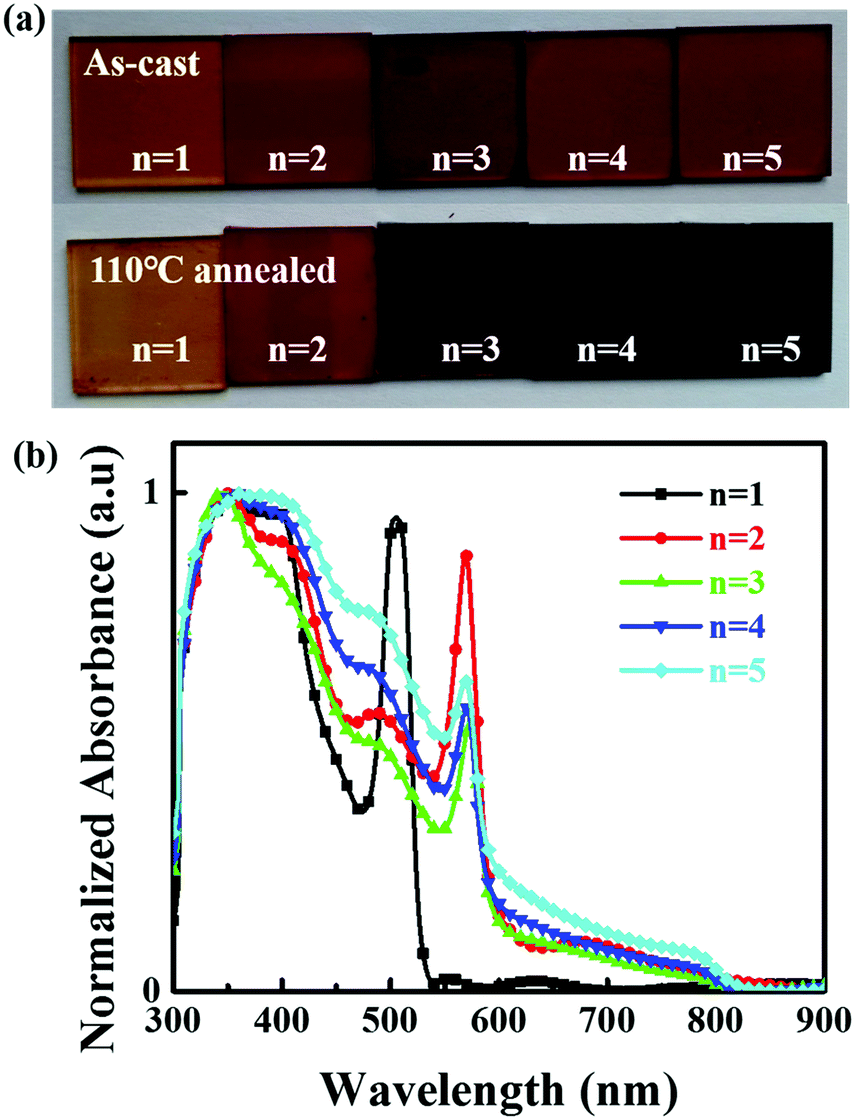 | ||
| Fig. 1 (a) Photos of the perovskite (BA)2(FA)n−1PbnI3n+1 films with different n values before and after thermal annealing at 110 °C for 15 min. (b) Normalized absorption spectra of the perovskite (BA)2(FA)n−1PbnI3n+1 films with different n values after thermal annealing. | ||
Considering the distinct absorption change for the n = 3 film and better stability for lower n values,41 the effect of thiourea on the optical properties of 2D perovskites was carefully studied using the (BA)2(FA)2Pb3I10 film. The mole ratio in the precursor is BAI:FAI:PbI2:thiourea = 2:2:3:x, where the x value varies from 0, 0.25, 0.5, 0.75 to 1. The colours of the as-cast films before annealing seem to be the same with different amounts of thiourea in the precursor, but become darker after annealing with increasing thiourea amount in the precursor. All the films look uniform and reflective except for the film with a thiourea mole proportion of 1 in the precursor (Fig. 2a). Adding too much thiourea in the precursor deteriorates the perovskite film and makes it rough. The optical absorption and photoluminescence (PL) spectra of the perovskite films are illustrated in Fig. 2b and c. Without thiourea in the precursor, the obtained film shows an absorption edge of 650 nm. When thiourea was added, exciton absorption peaks shifted slightly and the absorption range extended gradually to 820 nm with more than 0.25 M thiourea. This could be attributed to the enhanced crystallinity and orientation in 2D perovskite films assisted by thiourea.39,40 The red shift (from 740 to 790 nm) of the PL emission peak after adding thiourea also suggests a reduced bandgap. Besides, at least two peaks can be found in PL spectra, which might be caused by the coexistence of crystal grains with various n values in 2D perovskite films. Such a phenomenon has already been reported in other 2D perovskites.42,43
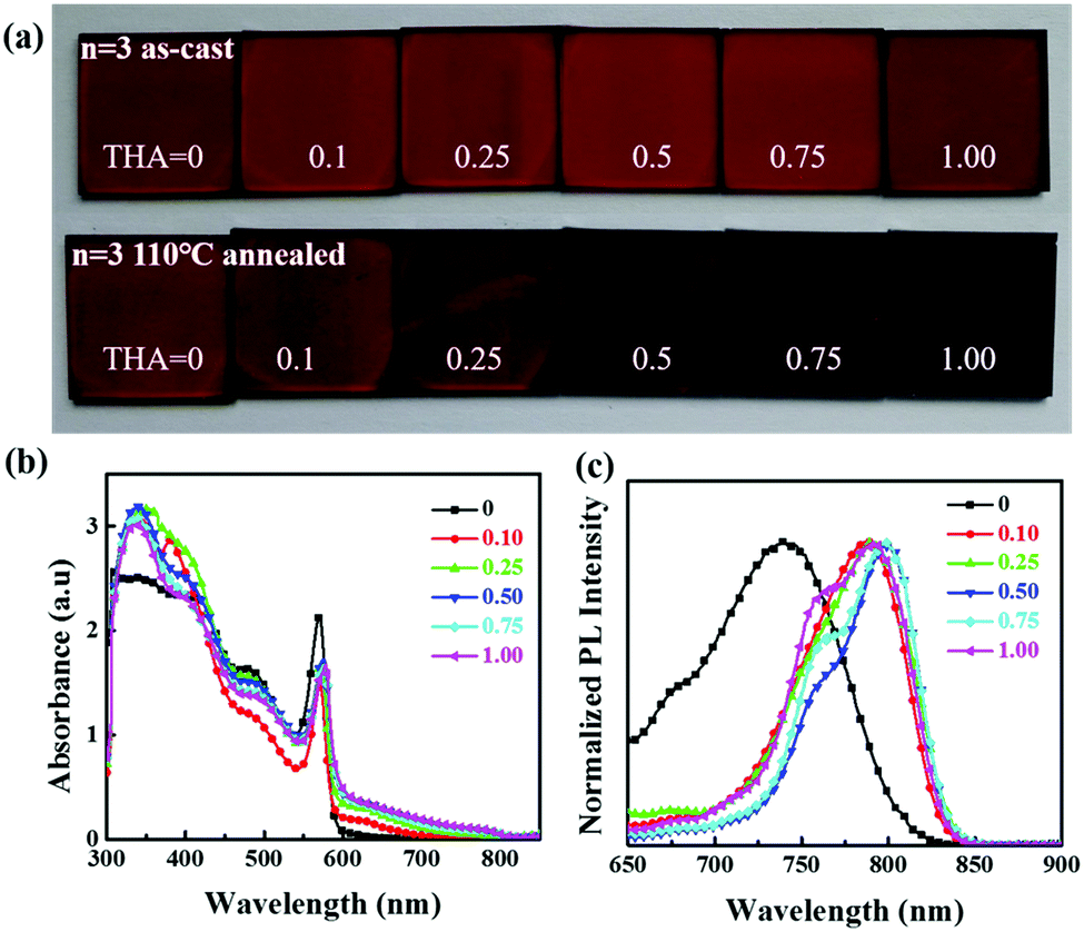 | ||
| Fig. 2 (a) Photos of (BA)2(FA)2Pb3I10 films fabricated with different precursors containing various amounts of thiourea before and after annealing; and (b) UV-vis absorption and (c) PL spectra of (BA)2(FA)2Pb3I10 films fabricated with different precursors containing various amounts of thiourea after thermal annealing. | ||
Scanning electron microscopy (SEM) was used to study the morphologies of the annealed (BA)2(FA)2Pb3I10 films fabricated with different precursors containing various amounts of thiourea (Fig. 3). As we can see, the grain size becomes larger upon increasing the amount of thiourea in the precursor. A fully covered surface with large grains can be obtained for films fabricated with precursors containing 0.25 and 0.5 M thiourea. Further increasing the amount of thiourea causes film cracks, which may lead to direct contact between the two electrodes in devices and make it challenging to fabricate working planar-type devices.44,45
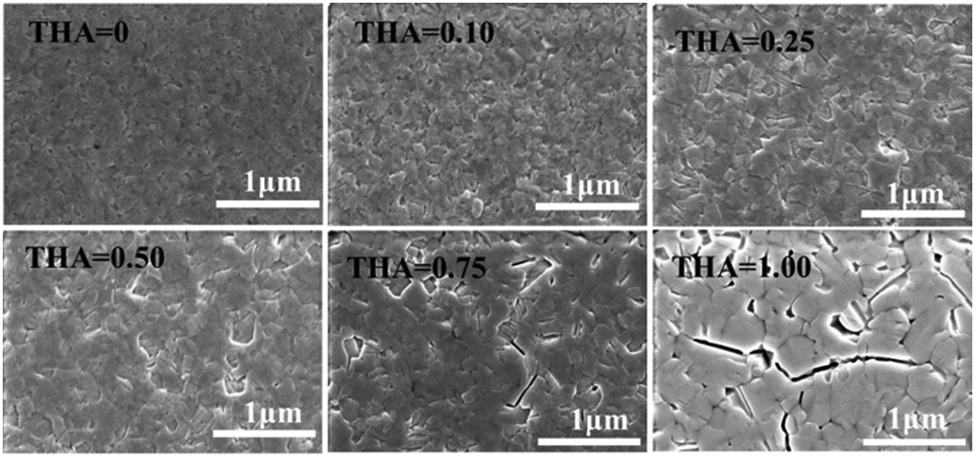 | ||
| Fig. 3 SEM images of the annealed (BA)2(FA)2Pb3I10 films fabricated with different precursors containing various amounts of thiourea. | ||
X-ray diffraction (XRD) patterns were obtained to investigate the crystallinity of the (BA)2(FA)2Pb3I10 perovskite films and are shown in Fig. 4. Three dominant planes were observed at diffraction angles of 14.05°, 28.23°, and 42.82°, representing the (BA)2(FA)2Pb3I10 crystallographic planes (111), (202), and (313), respectively, in all films.46 The intensities of the peaks increase linearly with increasing amount of thiourea, suggesting that the addition of thiourea favours perovskite crystallization.
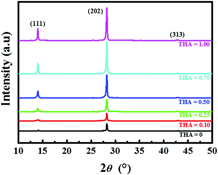 | ||
| Fig. 4 XRD patterns of (BA)2(FA)2Pb3I10 films fabricated with different precursors containing various amounts of thiourea. | ||
Grazing-incidence wide-angle X-ray scattering (GIWAXS) measurements were conducted to investigate the perovskite thin film crystallization and orientation on the substrates (Fig. 5). More structural features were observed in 2D diffraction patterns. In-plane and out-of-plane line cut profiles are shown in Fig. 5e. Both thermal annealing and thiourea addition had significant effects on the crystalline behaviour. The as-cast thin film without thiourea showed crystalline features of the perovskite (111) crystalline plane in both the in-plane and out-of-plane directions. There were other diffraction signals from other crystalline forms (∼0.3 A−1 and ∼0.6 A−1 diffraction peaks, etc.), whose structure is hard to determine from limited information. These can be complicated crystals containing solvent or other stoichiometric compounds. Thermal annealing significantly enhanced diffraction signals, indicating better crystallinity, which agreed well with XRD results (Fig. S2, ESI†). Yet thin films still take multiple crystalline forms, indicating a poor chemical quality, which would affect photovoltaic performances. Adding a small amount of thiourea could modify the crystalline packing of the perovskite material. Although the as-cast thin film was still a mixed crystalline packing, the 0.3 A−1 and 0.6 A−1 diffractions showed quite prominent changes both in shape and in orientation. More importantly, the thin film with 0.5 M thiourea under thermal annealing showed quite a clean perovskite crystalline form in which the 0.3 A−1 and 0.6 A−1 diffraction peaks mostly disappeared. The perovskite crystal (111) plane showed a prominent orientation in the out-of-plane direction, with also some preferences in the in-plane direction. The vertical alignment of the (111) crystal plane is preferred in 2D perovskite thin films, which show better electronic properties as shown in previous publications.19 These results revealed the two-fold function of the thiourea moiety in thin film fabrication. It should serve as the chelating agent that helps the material mixture to form 2D perovskites. It also integrated into those unknown crystals, making them unstable and ready to change into 2D perovskites under thermal annealing. The (111) crystal plane in the best performing thin film showed a much higher intensity in the out-of-plane direction than in the in-plane direction by a ratio about 5:1, indicating a good preferred orientation of 2D perovskite thin films. The improved crystal quality and crystallinity gave rise to better electronic and photon-to-electron conversion efficiency that will be shown in further discussion.
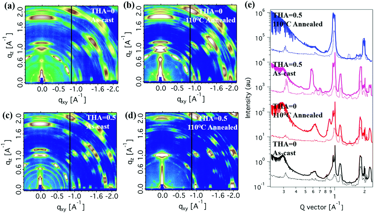 | ||
| Fig. 5 Grazing-incidence wide-angle X-ray scattering (GIWAXS) images of the as-cast films fabricated with the precursor without thiourea before (a) and after annealing (b); and with the precursor with 0.5 M thiourea before (c) and after annealing (d). (e) 1D in-plane and out-of-plane X-ray profiles extracted from GIWAXS. | ||
The hole and electron mobilities of (BA)2(FA)2Pb3I10 films without or with 0.5 M thiourea in precursors were measured using the space charge limited current (SCLC) method (see Fig. S3, ESI†). The device structures are ITO/SnO2/(BA)2(FA)2Pb3I10/PC61BM/BCP/Ag for electron-only devices and ITO/PEDOT:PSS/(BA)2(FA)2Pb3I10/PTAA/MoO3/Ag for hole-only devices. Table 1 lists the measured charge carrier mobilities. Owing to the improved crystallinity and orientation of the perovskite films after adding thiourea, the electron mobility is (8.56 ± 2.40) × 10−4 cm2 V−1 s−1 for the (BA)2(FA)2Pb3I10 film with 0.5 M thiourea, which is 80 times higher than that for the film without thiourea ((1.09 ± 0.61) × 10−5 cm2 V−1 s−1). On the other hand, the hole mobility of the (BA)2(FA)2Pb3I10 film with 0.5 M thiourea is (4.80 ± 1.79) × 10−4 cm2 V−1 s−1, which is three orders of magnitude higher than that of the film without thiourea ((7.24 ± 2.26) × 10−7 cm2 V−1 s−1). The enormous enhanced charge carrier mobilities and more balanced electron and hole mobilities are helpful for charge collection and reducing recombination.
| Thiourea [M] | μ [cm2 V−1 s−1] | μ e/μh | |
|---|---|---|---|
| 0.5 | μ e | (8.56 ± 2.40) × 10−4 | 1.78 |
| μ h | (4.80 ± 1.79) × 10−4 | ||
| 0 | μ e | (1.09 ± 0.61) × 10−5 | 15.05 |
| μ h | (7.24 ± 2.26) × 10−7 | ||
The phase and ambient stabilities of the prepared (BA)2(FA)2Pb3I10 film are investigated. Fig. 6 shows the normalized XRD patterns for unencapsulated films processed from the precursor with 0.5 M thiourea. The films were kept in a humidity controlled cabinet with a relative humidity of 55 ± 5%. The intensities of three dominant peaks at 14.05°, 28.23° and 42.82° remained almost unchanged after one week and no other peak appeared. After two weeks, the film was still black, and only a weak peak at 12.7° was observed, which belongs to PbI2. This indicates that the yellow phase transformation in the (BA)2(FA)2Pb3I10 film is significantly retarded and with only a relatively small amount of the perovskite degraded into PbI2 after two weeks under ambient conditions.
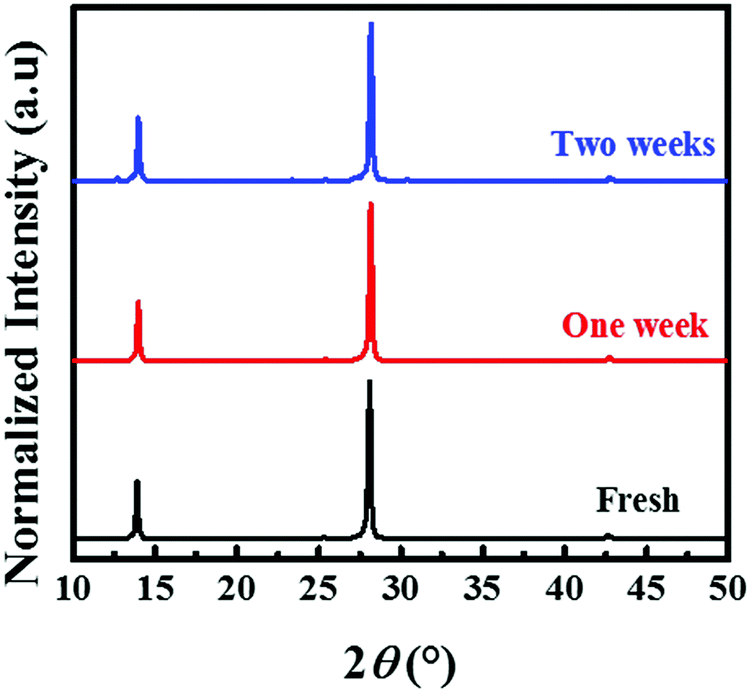 | ||
| Fig. 6 XRD patterns of (BA)2(FA)2Pb3I10 films at a relative humidity of 55 ± 5% with different aging times. | ||
The uniform, highly orientated, and moisture-stable 2D perovskite thin films with a small bandgap enable their use in planar photovoltaic devices. Solar cells in a planar heterojunction with an ITO/PEDOT:PSS/(BA)2(FA)2Pb3I10/PC61BM/BCP/Ag architecture were constructed to explore the photovoltaic performance of (BA)2(FA)2Pb3I10 (Fig. 7a). A cross-sectional SEM image indicates a densely-grained uniform (BA)2(FA)2Pb3I10 perovskite layer in the device. The current density–voltage (J–V) curves of the best device based on (BA)2(FA)2Pb3I10 films fabricated with different precursors containing various amounts of thiourea are shown in Fig. 7b and the corresponding parameters are summarized in Table 2. We can see that the short-circuit current density (JSC) significantly increases from 2.08 mA cm−2 to 11.89 mA cm−2 when 0.5 M thiourea is added to the precursor. This could be attributed to the highly oriented crystal domains and the reduced bandgap. On the other hand, VOC and FF slightly decrease especially for the devices based on the film processed from precursors with 0.75 and 1 M thiourea. This is because too much thiourea causes incomplete surface coverage as shown in Fig. 3, leading to direct contact of two electrodes. Our champion device based on the (BA)2(FA)2Pb3I10 film with optimized 0.5 M thiourea in the precursor shows a PCE of 6.88% in the forward scan as shown in Fig. 7c, with a VOC of 0.98 V, a JSC of 11.89 mA cm−2 and an FF of 0.59, under AM1.5G illumination. The device shows only a slight hysteresis with a PCE of 6.53% in the reverse scan, with a VOC of 0.99 V, a JSC of 11.87 mA cm−2 and an FF of 0.56. The FF values of the devices fabricated with more thiourea are lower than that without thiourea, which could be attributed to the increased charge recombination or leakage current caused by the increased surface roughening of the perovskite films with more thiourea (Fig. S4, ESI†).47–49 The steady-state PCE (5.93%) after 600s, shown in Fig. 7e, is close to the value obtained from the J–V scan. The external quantum efficiency (EQE) spectrum in Fig. 7d shows a wide range of absorption from 300 nm to 820 nm, which matches well with that of the UV-vis absorption spectrum. The integrated JSC from the EQE spectrum is calculated to be 12.48 mA cm−2, which agrees well with the value measured from the J–V curve.
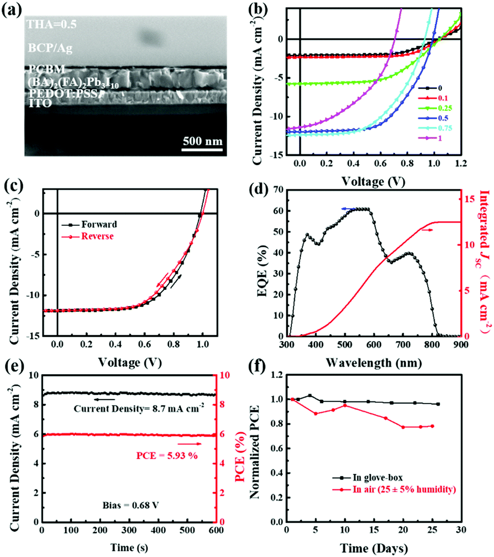 | ||
| Fig. 7 (a) Cross-sectional SEM image of a device with (BA)2(FA)2Pb3I10 fabricated from the precursor with 0.5 M thiourea. (b) J–V curves of the devices with (BA)2(FA)2Pb3I10 films fabricated with different precursors containing various amounts of thiourea. (c) J–V curves and (d) EQE spectrum of the best device with (BA)2(FA)2Pb3I10 films fabricated with the precursor containing 0.5 M thiourea. (e) Stabilized photocurrent measurement of the best device under 1 Sun illumination. (f) Evolution of the device performance as a function of time. | ||
| Thiourea [M] | V OC [V] | J SC [mA cm−2] | FF | PCE (average) [%] |
|---|---|---|---|---|
| 0 | 1.02 | 2.08 | 0.62 | 1.31 (1.19) |
| 0.10 | 1.04 | 2.33 | 0.65 | 1.56 (1.37) |
| 0.25 | 1.03 | 5.76 | 0.54 | 3.22 (3.00) |
| 0.50 | 0.98 | 11.89 | 0.59 | 6.88 (5.27) |
| 0.75 | 0.92 | 12.37 | 0.53 | 6.00 (5.22) |
| 1.00 | 0.70 | 11.38 | 0.42 | 3.36 (2.09) |
We performed a long-term stability test for our solar cell devices both in a N2 atmosphere and in a moisture controlled atmosphere. As shown in Fig. 7f, the PCE of the unencapsulated device remains almost unchanged after 25 days of storage in a N2 atmosphere. When the device was stored in air with a relative humidity of 25 ± 5%, it retained 80% of its original PCE after 25 days. A stability test under a higher relative humidity of 55 ± 5% for the unencapsulated device based on (BA)2(FA)2Pb3I10 was also conducted, and the results are summarized in Fig. S5 (ESI†). At least 70% of the initial PCE was retained after 9 days of storage under a relative humidity of 55 ± 5%. All these results indicate good stability against moisture and oxygen for (BA)2(FA)2Pb3I10 based solar cells.
Conclusion
In summary, we synthesized small bandgap 2D perovskites (BA)2(FA)n−1PbnI3n+1 (n = 1–5) to extend the absorption edge to longer wavelengths. (BA)2(FA)2Pb3I10 with a small bandgap of 1.51 eV was demonstrated, which is much smaller than 1.89 eV of the MA based counterpart (BA)2(MA)2Pb3I10. (BA)2(FA)2Pb3I10 films show good phase and ambient stability. We also find that thiourea as an additive can effectively tune the orientation of the perovskites, making the crystallographic planes of the inorganic perovskite component have a strongly preferential out-of-plane alignment with respect to the contacts in planar solar cells to facilitate efficient charge transport. Thus highly efficient and stable inverted PVSCs with a planar structure of ITO/PEDOT:PSS/(BA)2(FA)2Pb3I10/PC61BM/BCP/Ag were fabricated. The best PCE of 6.88% with only a slight hysteresis was demonstrated. As far as we know, our result is among the highest PCE values for FA based 2D perovskite solar cells. The unencapsulated device retains 80% of its initial efficiency after storing in air for 25 days with a relative humidity of 25 ± 5%, indicating good stability against moisture and oxygen.Experimental
Materials
A perovskite precursor solution was prepared by mixing BAI (99%, TCI), FAI (99%, MaterWin), PbI2 (99%, Alfa Aesar), and (NH2)2CS (99%, Sigma) with a molar ratio of 2:2:3:x (x = 0, 0.1, 0.25, 0.5, 0.75, 1, referred to as THA = 0, THA = 0.1, THA = 0.25, THA = 0.5, THA = 0.75, and THA = 1, respectively) in 1 mL of DMF (99%, Aldrich), and stirred overnight in a N2 glovebox at 70 °C. Poly(3,4-ethylenedioxythiophene):poly(styrene-sulfonate) (PEDOT:PSS, PAI4083) aqueous solution was purchased from Baytron. (6,6)-Phenyl-C61-butyric acid methyl ester (PC61BM, 99.5%) was purchased from Lumtec. Bathocuproine (BCP, 99%) was purchased from J&K. Silver (Ag, 99.99%) was purchased from Alfa Aesar. All reagents and solvents were directly used without further purification, if not specified.
Device fabrication
ITO-Coated glass (sheet resistance ≤10 Ω cm−2, MaterWin) was cleaned consecutively in detergent, acetone, isopropanol, and ethanol ultrasonic baths for 15 min, respectively. The ITO glass was treated with UV-Ozone for 15 min. A thin layer of PEDOT:PSS was spin-coated onto the cleaned ITO at 3000 rpm for 40 s, and annealed in a vacuum oven at 140 °C for 25 min. Then the substrate was transferred into a glovebox for active layer deposition and further device fabrication. A perovskite active layer was spin-coated at 6000 rpm for 60 s onto the PEDOT:PSS coated ITO (ITO/PEDOT:PSS) substrate from 30 μL of the perovskite precursor solution at a concentration of 1 M (based on PbI2), and annealed at 110 °C for 15 min. After deposition of the perovskite active layer, PC61BM (20 mg mL−1 in chlorobenzene) and BCP (0.5 mg mL−1 in absolute ethanol) layers were deposited subsequently at 1500 rpm for 45 s and 3000 rpm for 30 s, respectively. The sample was then transferred into a vacuum chamber for further deposition of Ag (100 nm) to finish the device fabrication process. The device area is defined to be 0.06 cm2 using a metal mask, whereas the total device area defined by the overlap of the electrodes was approximately 0.12 cm2.Characterization
The chemical compositions of perovskite films before and after thermal annealing were compared using Fourier transform infrared (FTIR) spectra obtained on a Nicolet 5700 IR spectrometer (Thermo Fisher) under the diffuse reflectance mode with the signal of air as the calibration background. The crystallographic properties of (BA)2(FA)n−1PbnI3n+1-based perovskite films were investigated using an Ultima IV diffractometer (Rigaku, graphite monochromatic, Cu-Kα radiation) at room temperature with a scanning rate of 10° min−1 over the Bragg angle range of 10.0°–50.0° (2θ). Film and device morphologies were studied using the scanning electron microscope (SEM) images obtained on an S-4800 field-emission scanning electron microscope (FESEM). Absorption spectra were recorded using a UV-2450 UV-visible spectrophotometer (Shimadzu). Grazing-incidence wide-angle X-ray scattering (GIWAXS) characterization of the 2D perovskite layer was performed at beamline 7.3.3, Advanced Light Source (ALS), Lawrence Berkeley National Lab (LBNL). The X-ray energy was 10 keV while operating in the top off mode. The scattering intensity was recorded on a 2D image plate (Pilatus 1M) with a pixel size of 172 mm (981 × 1043 pixels). The sample-to-detector distance was about 300 mm. The incidence angle was chosen to be 0.6°. The J–V characteristics were measured with Keithley 2400 measurement source units with the devices maintained at room temperature in the glovebox. The photovoltaic response was measured using a calibrated solar simulator (Enli Technology) at 100 mW cm−2, and the light intensity was calibrated with a standard photovoltaic reference cell. The EQE spectrum was measured using a QE-R Model of Enli Technology. The (BA)2(FA)2Pb3I10-based perovskite films were kept in a humidity controlled cabinet (Hr = (55 ± 5%), Bossmen, PR1852(A)-SH) for humidity–stability measurements. The stabilities of the unsealed devices were tested under different conditions including a N2 atmosphere (glovebox) and air with Hr = 25 ± 5% and 55 ± 5%.Conflicts of interest
There are no conflicts to declare.Acknowledgements
This work was supported by the National Natural Science Foundation of China (Grant No. 51620105006), the Major State Basic Research Development Program (2014CB643503), the International Science and Technology Cooperation Program of China (ISTCP) (Grant No. 2016YFE0102900), the Zhejiang Province Natural Science Foundation (Grant No. LR15E030001), and the National Science Foundation for Post-doctoral Scientists of China (2015M580512).References
- A. Kojima, K. Teshima, Y. Shirai and T. Miyasaka, J. Am. Chem. Soc., 2009, 131, 6050–6051 CrossRef CAS PubMed.
- M. M. Lee, J. Teuscher, T. Miyasaka, T. N. Murakami and H. J. Snaith, Science, 2012, 338, 643–647 CrossRef CAS PubMed.
- S. D. Stranks, G. E. Eperon, G. Grancini, C. Menelaou, M. J. Alcocer, T. Leijtens, L. M. Herz, A. Petrozza and H. J. Snaith, Science, 2013, 342, 341–344 CrossRef CAS PubMed.
- G. Xing, N. Mathews, S. Sun, S. S. Lim, Y. M. Lam, M. Gratzel, S. Mhaisalkar and T. C. Sum, Science, 2013, 342, 344–347 CrossRef CAS PubMed.
- H. S. Kim, C. R. Lee, J. H. Im, K. B. Lee, T. Moehl, A. Marchioro, S. J. Moon, R. Humphry-Baker, J. H. Yum, J. E. Moser, M. Gratzel and N. G. Park, Sci. Rep., 2012, 2, 591 CrossRef PubMed.
- J. Burschka, N. Pellet, S. J. Moon, R. Humphry-Baker, P. Gao, M. K. Nazeeruddin and M. Gratzel, Nature, 2013, 499, 316–319 CrossRef CAS PubMed.
- V. D'Innocenzo, G. Grancini, M. J. Alcocer, A. R. Kandada, S. D. Stranks, M. M. Lee, G. Lanzani, H. J. Snaith and A. Petrozza, Nat. Commun., 2014, 5, 3586 Search PubMed.
- V. Gonzalez-Pedro, E. J. Juarez-Perez, W. S. Arsyad, E. M. Barea, F. Fabregat-Santiago, I. Mora-Sero and J. Bisquert, Nano Lett., 2014, 14, 888–893 CrossRef CAS PubMed.
- C. S. Ponseca, Jr., T. J. Savenije, M. Abdellah, K. Zheng, A. Yartsev, T. Pascher, T. Harlang, P. Chabera, T. Pullerits, A. Stepanov, J. P. Wolf and V. Sundstrom, J. Am. Chem. Soc., 2014, 136, 5189–5192 CrossRef PubMed.
- C. Huang, W. Fu, C.-Z. Li, Z. Zhang, W. Qiu, M. Shi, P. Heremans, A. K. Y. Jen and H. Chen, J. Am. Chem. Soc., 2016, 138, 2528–2531 CrossRef CAS PubMed.
- W. Fu, J. Yan, Z. Zhang, T. Ye, Y. Liu, J. Wu, J. Yao, C.-Z. Li, H. Li and H. Chen, Sol. Energy Mater. Sol. Cells, 2016, 155, 331–340 CrossRef CAS.
- L. Zuo, Z. Gu, T. Ye, W. Fu, G. Wu, H. Li and H. Chen, J. Am. Chem. Soc., 2015, 137, 2674–2679 CrossRef CAS PubMed.
- M. M. Tavakoli, A. Simchi, X. Mo and Z. Fan, Mater. Chem. Front., 2017, 1, 1520–1525 RSC.
- F. Meng, K. Liu, S. Dai, J. Shi, H. Zhang, X. Xu, D. Li and X. Zhan, Mater. Chem. Front., 2017, 1, 1079–1086 RSC.
- B. Huang, Q. Fu, Q. Ai, L. Tan, L. Chen and Y. Chen, Mater. Chem. Front., 2017, 1, 1179–1184 RSC.
- http://https://www.nrel.gov/pv/assets/images/efficiency-chart.png .
- I. C. Smith, E. T. Hoke, D. Solis-Ibarra, M. D. McGehee and H. I. Karunadasa, Angew. Chem., Int. Ed. Engl., 2014, 53, 11232–11235 CrossRef CAS PubMed.
- D. H. Cao, C. C. Stoumpos, O. K. Farha, J. T. Hupp and M. G. Kanatzidis, J. Am. Chem. Soc., 2015, 137, 7843–7850 CrossRef CAS PubMed.
- H. Tsai, W. Nie, J.-C. Blancon, C. C. Stoumpos, R. Asadpour, B. Harutyunyan, A. J. Neukirch, R. Verduzco, J. J. Crochet, S. Tretiak, L. Pedesseau, J. Even, M. A. Alam, G. Gupta, J. Lou, P. M. Ajayan, M. J. Bedzyk, M. G. Kanatzidis and A. D. Mohite, Nature, 2016, 536, 312–316 CrossRef CAS PubMed.
- L. Zhang, M. G. Ju and W. Liang, Phys. Chem. Chem. Phys., 2016, 18, 23174–23183 RSC.
- Y. Wu, X. Yang, W. Chen, Y. Yue, M. Cai, F. Xie, E. Bi, A. Islam and L. Han, Nat. Energy, 2016, 1, 16148 CrossRef CAS.
- N. Li, Z. Zhu, C.-C. Chueh, H. Liu, B. Peng, A. Petrone, X. Li, L. Wang and A. K. Y. Jen, Adv. Energy Mater., 2017, 7, 1601307 CrossRef.
- D. H. Cao, C. C. Stoumpos, T. Yokoyama, J. L. Logsdon, T.-B. Song, O. K. Farha, M. R. Wasielewski, J. T. Hupp and M. G. Kanatzidis, ACS Energy Lett., 2017, 2, 982–990 CrossRef.
- Y. Chen, Y. Sun, J. Peng, W. Zhang, X. Su, K. Zheng, T. Pullerits and Z. Liang, Adv. Energy Mater., 2017, 7, 1700162 CrossRef.
- Y. Liao, H. Liu, W. Zhou, D. Yang, Y. Shang, Z. Shi, B. Li, X. Jiang, L. Zhang, L. N. Quan, R. Quintero-Bermudez, B. R. Sutherland, Q. Mi, E. H. Sargent and Z. Ning, J. Am. Chem. Soc., 2017, 139, 6693–6699 CrossRef CAS PubMed.
- C. C. Stoumpos, D. H. Cao, D. J. Clark, J. Young, J. M. Rondinelli, J. I. Jang, J. T. Hupp and M. G. Kanatzidis, Chem. Mater., 2016, 28, 2852–2867 CrossRef CAS.
- B.-E. Cohen, M. Wierzbowska and L. Etgar, Adv. Funct. Mater., 2017, 27, 1604733 CrossRef.
- M. Lyu, M. Zhang, N. A. Cooling, Y. Jiao, Q. Wang, J.-H. Yun, B. Vaughan, G. Triani, P. Evans, X. Zhou, K. Feron, A. Du, P. Dastoor and L. Wang, Sci. Bull., 2016, 61, 1558–1562 CrossRef CAS.
- N. Pellet, P. Gao, G. Gregori, T. Y. Yang, M. K. Nazeeruddin, J. Maier and M. Gratzel, Angew. Chem., Int. Ed. Engl., 2014, 53, 3151–3157 CrossRef CAS PubMed.
- W. S. Yang, J. H. Noh, N. J. Jeon, Y. C. Kim, S. Ryu, J. Seo and S. I. Seok, Science, 2015, 348, 1234–1237 CrossRef CAS PubMed.
- Q. Han, S. H. Bae, P. Sun, Y. T. Hsieh, Y. M. Yang, Y. S. Rim, H. Zhao, Q. Chen, W. Shi, G. Li and Y. Yang, Adv. Mater., 2016, 28, 2253–2258 CrossRef CAS PubMed.
- S. Yang, W. Liu, L. Zuo, X. Zhang, T. Ye, J. Chen, C.-Z. Li, G. Wu and H. Chen, J. Mater. Chem. A, 2016, 4, 9430–9436 CAS.
- Y. Guo, W. Sato, K. Shoyama, H. Halim, Y. Itabashi, R. Shang and E. Nakamura, J. Am. Chem. Soc., 2017, 139, 9598–9604 CrossRef CAS PubMed.
- D. P. McMeekin, Z. Wang, W. Rehman, F. Pulvirenti, J. B. Patel, N. K. Noel, M. B. Johnston, S. R. Marder, L. M. Herz and H. J. Snaith, Adv. Mater., 2017, 29 Search PubMed.
- Y. Wu, F. Xie, H. Chen, X. Yang, H. Su, M. Cai, Z. Zhou, T. Noda and L. Han, Adv. Mater., 2017, 29 CAS.
- H. Zhang, J. Cheng, D. Li, F. Lin, J. Mao, C. Liang, A. K. Jen, M. Gratzel and W. C. Choy, Adv. Mater., 2017, 29 Search PubMed.
- X. Zhang, G. Wu, S. Yang, W. Fu, Z. Zhang, C. Chen, W. Liu, J. Yan, W. Yang and H. Chen, Small, 2017, 13, 1700611 CrossRef PubMed.
- C. B. Fei, B. Li, R. Zhang, H. Y. Fu, J. J. Tian and G. Z. Cao, Adv. Energy Mater., 2017, 7, 1602017 CrossRef.
- J. W. Lee, H. S. Kim and N. G. Park, Acc. Chem. Res., 2016, 49, 311–319 CrossRef CAS PubMed.
- C. Fei, B. Li, R. Zhang, H. Fu, J. Tian and G. Cao, Adv. Energy Mater., 2017, 7, 1602017 CrossRef.
- L. N. Quan, M. Yuan, R. Comin, O. Voznyy, E. M. Beauregard, S. Hoogland, A. Buin, A. R. Kirmani, K. Zhao, A. Amassian, D. H. Kim and E. H. Sargent, J. Am. Chem. Soc., 2016, 138, 2649–2655 CrossRef CAS PubMed.
- M. Yuan, L. N. Quan, R. Comin, G. Walters, R. Sabatini, O. Voznyy, S. Hoogland, Y. Zhao, E. M. Beauregard, P. Kanjanaboos, Z. Lu, D. H. Kim and E. H. Sargent, Nat. Nanotechnol., 2016, 11, 872–877 CrossRef CAS PubMed.
- N. Wang, L. Cheng, R. Ge, S. Zhang, Y. Miao, W. Zou, C. Yi, Y. Sun, Y. Cao, R. Yang, Y. Wei, Q. Guo, Y. Ke, M. Yu, Y. Jin, Y. Liu, Q. Ding, D. Di, L. Yang, G. Xing, H. Tian, C. Jin, F. Gao, R. H. Friend, J. Wang and W. Huang, Nat. Photonics, 2016, 10, 699–704 CrossRef CAS.
- A. Fakharuddin, F. Di Giacomo, I. Ahmed, Q. Wali, T. M. Brown and R. Jose, J. Power Sources, 2015, 283, 61–67 CrossRef CAS.
- T. B. Song, Q. Chen, H. P. Zhou, S. Luo, Y. Yang, J. B. You and Y. Yang, Nano Energy, 2015, 12, 494–500 CrossRef CAS.
- D. B. Mitzi, J. Mater. Chem., 2004, 14, 2355–2365 RSC.
- B. Qi and J. Wang, Phys. Chem. Chem. Phys., 2013, 15, 8972–8982 RSC.
- M. S. Kim, B. G. Kim and J. Kim, ACS Appl. Mater. Interfaces, 2009, 1, 1264–1269 CAS.
- V. Djara and J. C. Bernède, Thin Solid Films, 2005, 493, 273–277 CrossRef CAS.
Footnotes |
| † Electronic supplementary information (ESI) available. See DOI: 10.1039/c7qm00472a |
| ‡ These authors contributed equally to this work. |
| This journal is © the Partner Organisations 2018 |