
Improving the moisture stability of perovskite solar cells by using PMMA/P3HT based hole-transport layers†
Soumya
Kundu
 and
Timothy L.
Kelly
*
and
Timothy L.
Kelly
*
Department of Chemistry, University of Saskatchewan, 110 Science Place, Saskatoon, SK S7N 5C9, Canada. E-mail: tim.kelly@usask.ca
First published on 31st October 2017
Abstract
In recent years, the performance of lead halide perovskite solar cells has increased dramatically, setting a record efficiency of 22.1%; however, their sensitivity towards water limits their utility and still needs to be addressed. While many different materials and methods are being developed to solve this problem, recent studies have suggested that modifications to the hole-transport layer can be effectively used to improve device stability. In this study, we report a new device architecture that makes use of a poly(3-hexylthiophene) (P3HT) nanowire network in a poly(methyl methacrylate) (PMMA) matrix as the hole-transport layer. The PMMA matrix imparts excellent resistance toward the ingress of both liquid and vapor-phase water, and leads to a large increase in the stability of the device. Using a combination of in situ absorbance spectroscopy, powder X-ray diffraction and device measurements, we have quantified the increase in device stability; optimized PMMA/P3HT layers can improve device lifetimes by an order of magnitude.
 Timothy L. Kelly | Timothy Kelly is an Associate Professor in the Department of Chemistry at the University of Saskatchewan, and holds a Tier 2 Canada Research Chair in Photovoltaics. He received his BSc degree in Chemistry from Memorial University of Newfoundland in 2005, and completed a PhD under the supervision of Prof. Michael Wolf at the University of British Columbia (2005–2009). From 2009–2011 he was an NSERC Post-doctoral Fellow in the laboratory of Prof. Michael Sailor at the University of California, San Diego. His research interests include perovskite solar cells, hard X-ray scattering techniques, organic electronics, and plasmonics. |
Introduction
Hybrid organic–inorganic metal halide perovskite solar cells (PSCs) have evolved exponentially since they were first reported in 2009 by Miyasaka et al.1 Over the space of just a few years, the power conversion efficiency (PCE) improved from 3.8% to 22.1%.1–7 The excellent PCE of these devices is mainly due to a unique combination of excellent optoelectronic properties, such as high charge carrier mobilities, direct band gaps, long charge carrier diffusion lengths, high absorption coefficients, and a relative insensitivity to trap states.8–13 Yet despite having high efficiencies and potentially low manufacturing costs, PSCs have some major drawbacks which must be addressed before commercialization. The main issue of PSCs is a lack of long-term stability with respect to environmental stresses such as humidity, oxygen, light, and heat. Conventional silicon solar cells can be purchased with a 20–30 year manufacturer warranty, whereas the performance of PSCs declines significantly over a period of weeks or days when stored in ambient air.14–23It is well documented that moisture plays a key role in the decomposition of methylammonium lead iodide (CH3NH3PbI3), which in turn results in the premature failure of PSCs.16–18,21,22,24–27 Upon exposure to high levels of moisture at room temperature, the dark brown CH3NH3PbI3 readily forms a colourless monohydrate phase (CH3NH3PbI3·H2O), wherein the water becomes hydrogen-bonded to the methylammonium cation. Upon further hydration, a dihydrate phase ((CH3NH3)4PbI6·2H2O) is formed alongside PbI2. While the first hydration step is at least partially reversible, once PbI2 has been formed, it tends to crystallize and phase separate, limiting any further reversibility and leading to cell failure.16,17,25
Numerous attempts have been made to improve the moisture stability of PSCs. The most obvious strategy is device encapsulation; while some level of device encapsulation will undoubtedly be required in commercial applications, in the absence of any further device stabilization, even a small pinhole could result in total device failure. Therefore, each component of the underlying device still needs to be stabilized. With interfacial photochemical reactions and ion migration resulting in degradation of the metal electrodes,28–31 one strategy has been to use more robust and hydrophobic electrode materials.32–39 Other approaches have aimed to improve the stability of the perovskite itself; this has been accomplished by using mixed-cation perovskites or by using cross-linkers such as alkylphosphonic acid ω-ammonium chlorides, polyethylene glycol, and tertiary and quaternary hydrophobic alkyl ammonium cations.40–45 Studies on electron-transport layers have also revealed the stabilizing nature of mesoscopic alumina or titania scaffolds.46–48 However, the use of hydrophobic hole-transport layers (HTLs) for protection is perhaps one of the most promising approaches.22,27,49–53 In the most common device architectures, the HTL lies between the perovskite absorber and the top electrode; effectively, it can serve as a secondary vapor barrier between the perovskite and its environment. As an example, Habisreutinger et al. employed a HTL made of polymer-functionalized single-walled carbon nanotubes (SWCNTs) in a poly(methyl methacrylate) (PMMA) matrix which demonstrated substantially improved device stability.22 One of the main drawbacks of this approach is a lack of scalability; the purification and functionalization of SWCNTs is extremely challenging synthetically, substantially increasing cost. In short, although tremendous effort has been devoted to improving the stability of PSCs, a cost-effective device with long-term stability remains elusive.
In this work, we employ a HTL composed of a poly(3-hexylthiophene) (P3HT) nanowire framework suspended in a PMMA matrix. This type of PMMA/P3HT composite has been previously used in organic electronic applications to improve air stability and for its mechanical strength,54–57 and here we exploit it as a vapor barrier between the external environment and the perovskite active layer (Fig. 1). A thin compact layer of P3HT efficiently collects holes from the perovskite, while the P3HT nanowire framework provides a percolation pathway for holes to effectively reach the metal top electrode. Meanwhile, the dense PMMA matrix blocks the ingress of water into the device, leading to devices whose lifetime is improved by an order of magnitude relative to P3HT controls.
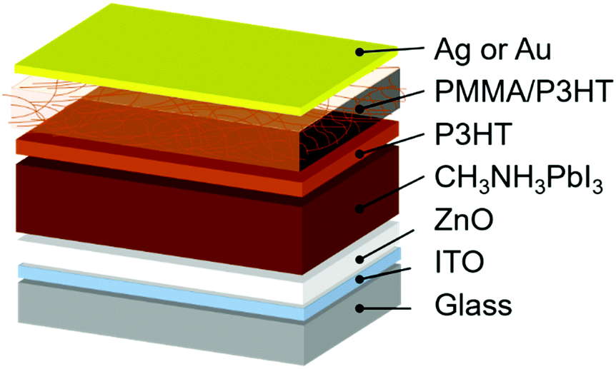 | ||
| Fig. 1 Schematic of the device architecture used in this study. The hole-transport layer consists of a thin, compact layer of P3HT, followed by a thicker layer of P3HT nanowires suspended in a PMMA matrix. | ||
Experimental section
P3HT nanowire synthesis
PMMA/P3HT polymer blends were prepared using previously reported procedures.55,58 P3HT and PMMA were added to a solvent mixture of chloroform/anisole (50![[thin space (1/6-em)]](https://www.rsc.org/images/entities/char_2009.gif) :50 v/v) in order to achieve a total polymer concentration of 10 mg mL−1. Four different samples were prepared, with PMMA to P3HT ratios (w/w) varying from 80:20 to 95:5. Then the mixture was placed on a programmable hot plate to dissolve at 70 °C overnight with continuous stirring. The solution was then gradually cooled to room temperature at 20 °C h−1 without stirring. The color of the solution changed from transparent red to dark brown, indicating the formation of P3HT nanowires. The solution was left undisturbed for 3 days before use.
:50 v/v) in order to achieve a total polymer concentration of 10 mg mL−1. Four different samples were prepared, with PMMA to P3HT ratios (w/w) varying from 80:20 to 95:5. Then the mixture was placed on a programmable hot plate to dissolve at 70 °C overnight with continuous stirring. The solution was then gradually cooled to room temperature at 20 °C h−1 without stirring. The color of the solution changed from transparent red to dark brown, indicating the formation of P3HT nanowires. The solution was left undisturbed for 3 days before use.
Solar cell fabrication
Solar cells were fabricated by following previously reported procedures.59,60 ITO-coated glass substrates were cleaned by sequentially sonicating them for 20 min in 2% Extran 300 detergent, acetone and isopropanol followed by drying in an oven at 120 °C for 2 h. Then a thin ZnO nanoparticle layer was spin coated onto the substrate at 3000 rpm for 30 s from a solution of 6 mg mL−1 in n-butanol. In order to produce a uniform film, the procedure was repeated three times. By using thermal evaporation, a thin layer of PbI2 (∼150 nm) was deposited at a base pressure of 2 × 10⁻⁶ mbar. Then the substrate was dipped into a solution of CH3NH3I in 2-propanol (10 mg mL−1) for 3 minutes, inside a glove-bag maintained at a relative humidity of ∼40%. The substrate was spin-dried at 3000 rpm for 25 s and then was kept for additional 10 minutes inside the bag. For control samples, a layer of P3HT was deposited by spin coating (1000 rpm for 30 s) from a solution containing 20 mg of P3HT, 1 mL of chlorobenzene, 3.4 μL of 4-tert-butylpyridine, and 6.8 μL of a lithium-bis(trifluoromethanesulfonyl)imide (Li-TFSI) solution (28 mg Li-TFSI/1 mL acetonitrile). For the PMMA/P3HT-based devices, first a thin layer of P3HT was deposited by spin coating (2000 rpm for 30 s) from a solution containing 20 mg of P3HT, 1 mL of chlorobenzene, 10 μL of 4-tert-butylpyridine, and 20.4 μL of the same Li-TFSI solution. Then the PMMA/P3HT blend was deposited by spin coating using a two-step spinning protocol (500 rpm for 10 s; 2500 rpm for 20 s). To produce different thicknesses of PMMA/P3HT layers, the spin speed of the second step was varied. Finally, either a silver or gold electrode was deposited by thermal evaporation at a base pressure of 2 × 10⁻⁶ mbar.Solar cell characterization
The performance of the devices was measured using a Keithley 2400 source-measure unit and a 450 W Class AAA solar simulator equipped with an AM 1.5G filter (Sol3A, Oriel Instruments) inside a nitrogen filled glovebox (<0.1 ppm O2 and H2O). The illumination intensity was adjusted to 100 mW cm−2 as determined by a standard silicon reference cell (91150V, Oriel Instruments). A non-reflective metal mask was used to define the effective area of the device to be 0.0708 cm2.Liquid water stability tests
Enough water was added to the top of a substrate to completely cover the surface (0.5–1.0 mL), and was left to stand for 1 minute. The devices were then blown dry in a stream of air, and reintroduced into the glovebox prior to testing.Water vapor stability tests
A stream of nitrogen carrier gas was bubbled through water in order to generate a stream of saturated (99 ± 1% relative humidity (RH)) water vapor. This flowed into either a custom-built sample holder (for in situ absorbance spectroscopy, Fig. S1, ESI†) or a gas-tight sample chamber (for device lifetime measurements, Fig. S2, ESI†). The RH and temperature were measured downstream of the sample chamber by an RH-USB humidity sensor (Omega). Devices were reintroduced into the glovebox prior to each measurement of their performance.Results and discussion
Device design
The device architecture used in the current study is shown in Fig. 1. We deposit the CH3NH3PbI3 absorber directly onto a compact ZnO electron-transport layer in a planar heterojunction design, as reported elsewhere.59,60 Onto this we deposit either a simple P3HT HTL (as a control), or a thin layer of P3HT, followed by a layer of P3HT nanowires in a PMMA matrix. The thin, compact P3HT layer is to ensure efficient hole extraction from the perovskite absorber; from there, the P3HT nanowire network provides a percolation pathway to the top electrode (either Ag or Au). The rationale behind the PMMA matrix is that it serves to prevent moisture ingress into the perovskite layer, thereby improving device stability. However, since the PMMA matrix is insulating, the hole-transporting characteristics of P3HT need to be carefully balanced against the protective properties of PMMA. We therefore prepared devices with four different PMMA/P3HT ratios: 95:5, 90:10, 85:15, and 80:20. We then investigated the effect of HTL composition on the layer morphology, device performance, and device lifetime.
PMMA/P3HT film morphology
In order for the PMMA/P3HT blend to work as a HTL, the P3HT must self-assemble into an interconnected nanowire network, through which holes can percolate from the P3HT collection layer to the metal electrode; as such, the morphology of the HTL is critical. AFM was used to assess the nanostructure of the four different PMMA/P3HT films on glass substrates (Fig. 2). Promisingly, even at the lowest P3HT loading (95:5 PMMA/P3HT), the appearance of nanowire-like structures can be observed in an otherwise smooth film (Fig. 2a), with nanowire widths of ∼10–20 nm. As the amount of P3HT in the blend is increased, the nanowire structure becomes more pronounced; the morphology of the 90:10 PMMA/P3HT sample appears to consist of the desired interconnected nanowire network, although this is also accompanied by an overall increase in surface roughness (Fig. 2b). The increase in surface roughness continues as the P3HT fraction is increased, with the 85:15 and 80:20 PMMA/P3HT films appearing to display less structured, but overall rougher, morphologies (Fig. 2c and d). At the highest P3HT loading, there is relatively little evidence of polymer nanowires, and the AFM image is consistent with simple phase separation into PMMA- and P3HT-rich domains.
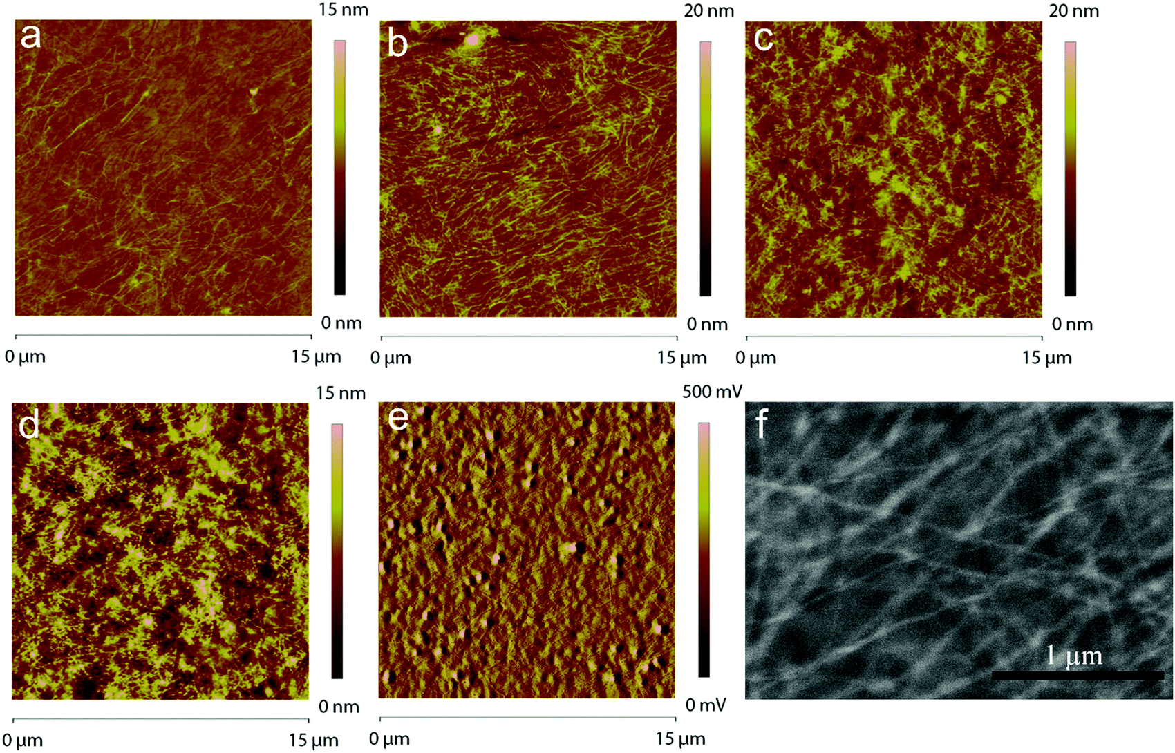 | ||
| Fig. 2 AFM images (height image) of PMMA/P3HT thin films on glass substrates, with varying PMMA/P3HT ratios: (a) 95:5; (b) 90:10; (c) 85:15; (d) 80:20. (e) AFM image (phase image) and (f) SEM image of 85:15 PMMA/P3HT films deposited on SiO2/ZnO/CH3NH3PbI3/P3HT substrates. | ||
PSCs were then fabricated using the four different PMMA/P3HT blends, using a ITO/ZnO/CH3NH3PbI3/P3HT/PMMA:P3HT/Ag architecture (Fig. 1). The device architecture is based on previous reports from our group, but with the addition of the PMMA:P3HT HTL.59,61 AFM was used to image the surface of the HTL (in areas lacking a metal top electrode). The rough surface of the underlying perovskite can still be seen in the AFM height images (Fig. S3, ESI†), suggesting conformal coverage by the HTL; the P3HT nanowires are also still visible in the AFM phase images, indicating that the nanowire morphology is maintained on the perovskite-coated substrate (Fig. 2e and Fig. S3, ESI†). SEM imaging validates these observations (Fig. 2f); at moderately high accelerating voltages, and with low Z samples, SEM is sensitive to sub-surface morphology, and the embedded P3HT nanowires can be clearly observed in the PMMA/P3HT film.
Device performance
Having established that the PMMA/P3HT HTLs had the desired nanowire morphology, we then evaluated their performance in PSCs, as compared to conventional P3HT HTLs. The devices based on pure P3HT HTLs had an average PCE of 9.1 ± 0.9%, with the champion device having a PCE of 11.0%, which is consistent with previous literature reports.60–64 Although this is lower than the efficiency of devices based on Li-TFSI-doped 2,2′,7,7′-tetrakis[N,N-di(4-methoxyphenyl)amino]-9,9′-spirobifluorene (Spiro-OMeTAD), numerous studies have now shown that Spiro-OMeTAD HTLs can lead to relatively short device lifetimes, whereas P3HT-based cells often show less rapid decomposition.18,22 In comparison with the P3HT-only control devices, PSCs based on the PMMA/P3HT HTLs had device characteristics that were highly dependent on the PMMA/P3HT raito (Fig. 3). When only a small amount of P3HT was added to the HTL (95:5 PMMA/P3HT), the devices performed quite poorly (best PCE of 5.6%); this is almost entirely due to a high series resistance (Fig. 3e), which limits both the fill factor and the short-circuit current density. This likely indicates poor connectivity between the P3HT nanowires; with no percolation pathway for holes, the PMMA matrix effectively limits the efficiency with which holes can be extracted. However, for the 90:10 PMMA/P3HT ratio, the interconnected nature of the nanowire array (Fig. 2b) provides for efficient hole transport, even through the PMMA matrix. As a result, these devices performed almost equivalently to the P3HT controls (PCE = 8.1 ± 0.9% vs. 9.1 ± 0.9% for the controls). As the P3HT concentration is increased further, the two polymers begin to phase separate more coarsely (Fig. 2c and d), resulting in a slow increase in series resistance and a concomitant decrease in FF and Jsc. In order to quantify the effect of hysteresis in our devices, we measured the J–V curves in both scan directions. For all devices, including both the P3HT controls and the PMMA/P3HT HTLs, the device efficiency was relatively independent of scan direction, indicating little hysteresis (Fig. S4, ESI†).
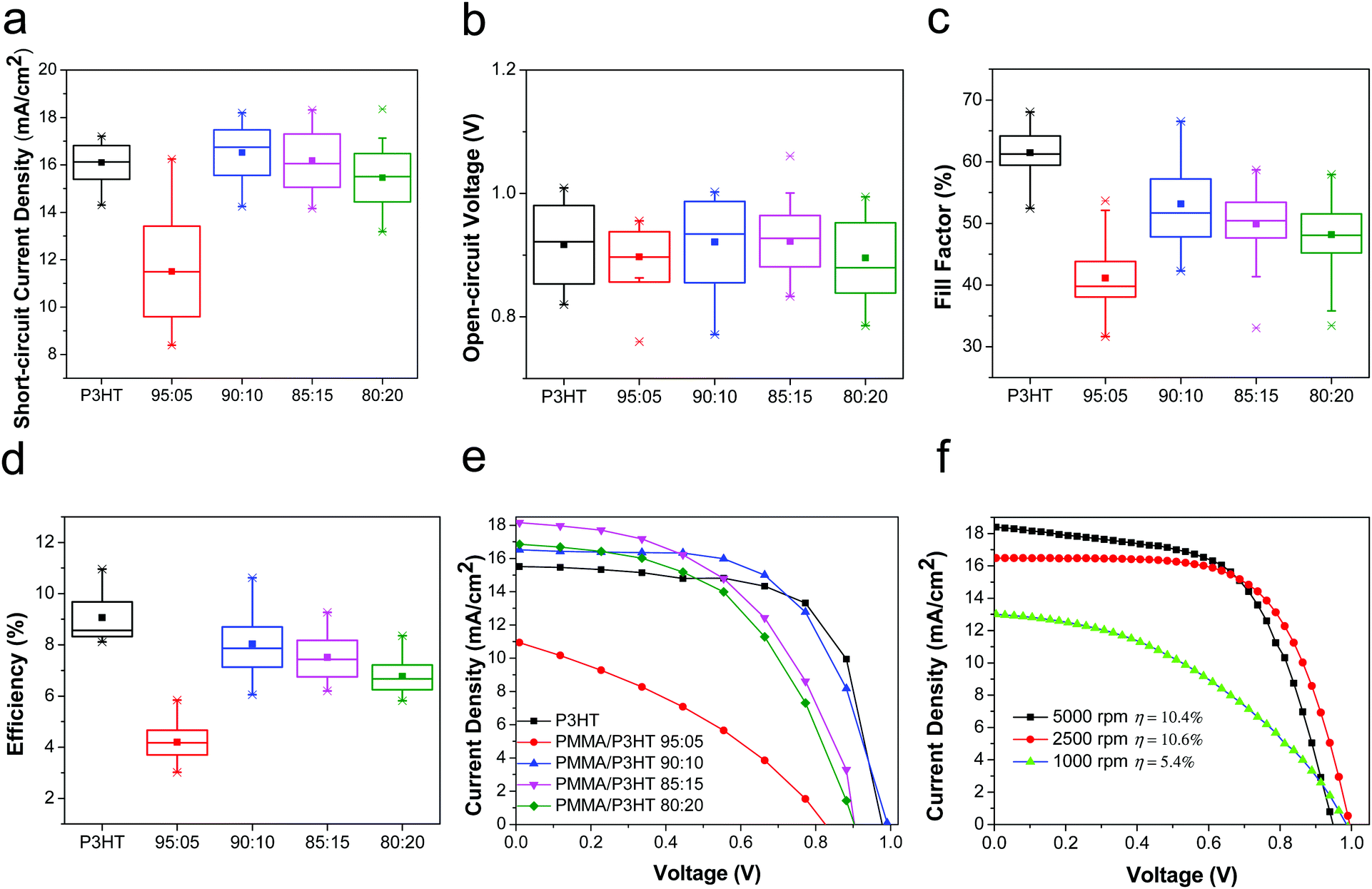 | ||
| Fig. 3 Cell performance parameters for devices made with varying HTLs: (a) Jsc; (b) Voc; (c) FF; (d) PCE. The crosses denote the 1st and 99th percentiles; the bars denote the maximum and minimum values; the box boundaries mark the 25th and 75th percentiles; the horizontal line denotes the median; the solid square denotes the mean. (e) J–V curve of the champion devices with the various HTLs, measured at a scan rate of 0.1 V s−1. (f) J–V curves for devices made with 90:10 PMMA/P3HT HTLs, deposited at different spin speeds. | ||
Since one of the primary functions of the PMMA/P3HT HTL is to provide an internal vapor barrier within the device stack, thicker layers would presumably impart better protection to the underlying perovskite; however, this comes at the cost of increased series resistance. For a fixed PMMA/P3HT ratio (90:10), the HTL was deposited at three different spin speeds (1000, 2500, and 5000 rpm), providing three different layer thicknesses. The PCEs of the champion devices from this study were 5.4, 10.6 and 10.4%, respectively (Fig. 3f). For the thickest HTL, the increase in series resistance (combined with a loss of shunt resistance) severely limits the cell performance; however, at 2500 rpm provide the best combination of a relatively low series resistance and a thicker vapor barrier, and these fabrication conditions were chosen for the subsequent stability studies.
Effect of liquid water on device performance
The deleterious effects of water on CH3NH3PbI3 have been well-established; liquid water rapidly destroys these materials by dissolution of CH3NH3I, leaving behind residual PbI2. Due to the excellent film forming properties and overall hydrophobicity (water contact angle = 103°)58 of the PMMA/P3HT layer, it is expected to form a water-impermeable coating over the CH3NH3PbI3. In order to study the resistance of our devices to liquid water, both our PMMA/P3HT-based and control devices (P3HT-only) were exposed to liquid water for 1 minute. Within a few seconds, the control sample had begun to degrade, and after 15 s it had completely decomposed, as evidenced by a color change from dark brown to yellow (Fig. S5, ESI†). In contrast, devices with PMMA/P3HT HTLs were unaffected (Fig. S5, ESI†). Both UV/vis spectroscopy (Fig. S6, ESI†) and powder X-ray diffraction (Fig. S7, ESI†) support this conclusion, with no change observed in either the absorption spectra or the diffraction patterns. The photovoltaic performance of the devices was also evaluated, both before and after water exposure (Fig. 4). Unsurprisingly, the P3HT-only control devices short-circuited after water exposure, and were virtually non-functional. In contrast, there was virtually no change in performance for any of the PMMA/P3HT-based devices. This is highly encouraging, as it suggests that even if the encapsulation on a commercial cell or module were to degrade, it may not immediately lead to catastrophic device failure.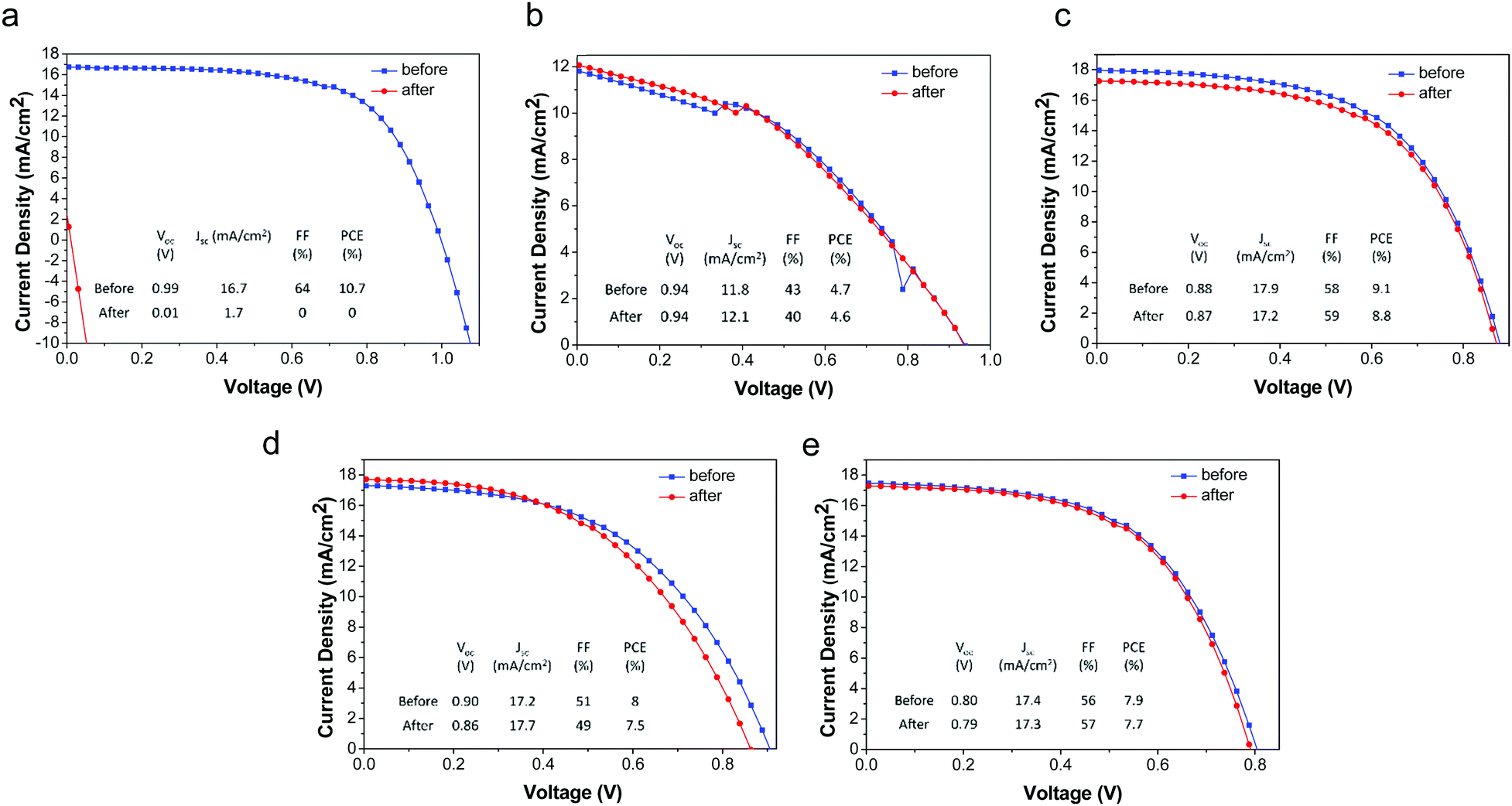 | ||
| Fig. 4
J–V curves for devices with various HTLs, measured before and after exposure to liquid water for 1 minute: (a) P3HT-only; (b) 95:5, (c) 90:10, (d) 85:15, (e) 80:20 PMMA/P3HT. Scans were performed at a scan rate of 0.83 V s−1 from forward bias to short-circuit. | ||
Effect of water vapor on device performance
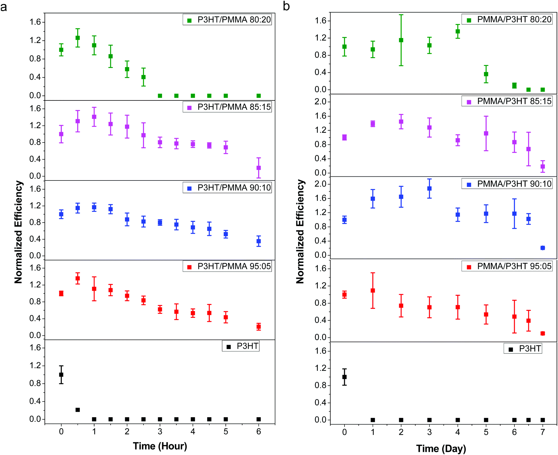
Although the penetration of liquid water into the device stack leads to the most rapid cell degradation, its high surface tension makes it relatively facile to exclude from the cell; in contrast, vapor-phase water is much more insidious, and even good barrier plastics have a non-zero moisture vapor transmission rate. Therefore, in order to better evaluate the performance of our PMMA/P3HT barrier HTL, we exposed our devices to various RH environments, and measured their performance as a function of time.As an initial test, we stored our devices in ambient air at 21–23 °C and 35–45% RH, and measured their photovoltaic performance at one day intervals (Fig. S8, ESI†). Even under these relatively mild conditions (room temperature and moderate RH), all of the P3HT control devices failed within 24 h. In contrast, the cells with PMMA/P3HT-based HTLs degraded much more slowly; after 96 h, all PMMA/P3HT-based devices retained ∼50% of their initial efficiency. While the devices with 80:20 and 85:15 PMMA/P3HT ratios had completely failed after 120 h, devices with higher PMMA ratios (90:10 and 95:05) were still functional, retaining ∼30–40% of their initial efficiency.
The rapid cell failure observed for the P3HT control samples is ascribed to halide ion migration from the CH3NH3PbI3 layer to the silver electrode; the iodide ions help facilitate the oxidation of the electrode, leading to cell failure.30,65 UV/vis spectroscopy and SEM were used to support this conclusion. The UV/vis spectra of the control devices showed that the band edge feature at 760 nm disappears upon aging, indicating decomposition of CH3NH3PbI3 (Fig. S9, ESI†). A basic visual inspection of the device also shows that the silver electrodes of the control devices were discoloured and corroded (Fig. S10, ESI†), which can also be observed by comparing SEM images of the electrodes before and after aging (Fig. S11, ESI†). High magnification SEM images show pronounced corrosion at the edges of the silver electrodes, with the appearance of cracks and non-metallic byproducts (as indicated by a change in electron contrast and an increase in charging). In contrast, the PMMA/P3HT devices all show only a minor decrease in absorbance across the UV/vis spectrum (Fig. S9, ESI†), and the silver electrodes remain shiny and metallic even after six days of aging (Fig. S10, ESI†), even under microscopic analysis (Fig. S12, ESI†). The PMMA may serve two functions here: (i) to prevent the ingress of water vapor into the perovskite layer, thereby reducing the mobility of iodide ions; and (ii), to block mobile iodide ions from leaving the perovskite layer and reaching the silver electrode. The better barrier properties of PMMA as compared to P3HT may be related to its molecular weight (350 kDa for PMMA, vs. 50 kDa for P3HT) or its more polar functional groups, which better bind water and/or iodide ions, slowing their transit through the layer.
Although a RH of ∼40% is typical of indoor conditions, modules deployed in the field will encounter a much wider range of water concentrations. We therefore carried out a more rigorous study where we subjected our devices to a 99 ± 1% RH environment. For this study, we flowed nitrogen carrier gas through a series of water-filled bubblers, producing a stream of saturated water vapor; this was then connected to the inlet of an air-tight sample chamber, while a RH sensor was connected to the outlet in order to validate the humidity inside the chamber (Fig. S2, ESI†). Since the silver electrode was identified as a critical component in the device degradation process, we carried out the study on devices built using both silver and gold electrodes.
As expected, the devices with silver electrodes decomposed at an accelerated rate in the 99% RH environment; the P3HT control devices retained only a third of their initial performance after 30 minutes of exposure, and completely short-circuited after 1 hour (Fig. 5a). Again, those devices incorporating a PMMA/P3HT barrier layer displayed enhanced lifetimes; with an 80:20 PMMA/P3HT ratio, the devices lasted for ∼2.5–3 h before failure, a five-fold increase in lifetime; with increasing PMMA loadings, the improvements are even more marked. The 90:10 PMMA/P3HT devices (which also displayed the best PCEs), retained ∼40% of their initial performance after 6 h of exposure to saturated water vapor. This represents over an order of magnitude increase in lifetime relative to the P3HT-only controls, and highlights the performance of the PMMA/P3HT HTL as an effective vapor barrier.
 | ||
| Fig. 5 Normalized power conversion efficiency as a function of time for perovskite solar cells with (a) silver electrodes and (b) gold electrodes, stored in a 99 ± 1% RH environment. Error bars denote plus-or-minus one standard deviation from the mean. | ||
Switching the top electrode from silver to gold provided a notable increase in device lifetime, and allowed a longer-term study to be carried out (Fig. 5b). Again, the devices based on P3HT controls degraded relatively quickly, with all devices shorting after <24 h of exposure. In contrast, the cells incorporating vapor barrier HTLs survived for ∼1 week in the 99% RH atmosphere. Again, the 80:20 PMMA/P3HT ratio provided the least resistance to water vapor, with cells failing after 4–5 days of exposure. This may be due to the more coarsely phase-separated morphology of these films (Fig. 2d); presumably, the large P3HT domains break up the more smooth, conformal, and less permeable PMMA coating, allowing for greater levels of moisture permeation. As the PMMA loading is increased, the devices last longer, with some of the best results obtained with a 90:10 PMMA/P3HT ratio. In this case, over the first few days of testing, we actually observed an increase in device performance, primarily due to an increase in photocurrent and fill factor. Our previous work has noted that non-zero RH levels during the perovskite deposition process can actually increase device performance due to better connectivity between individual crystalline grains;60 in this case, low levels of moisture may actually be solvent-annealing the perovskite layer, resulting in improved performance. However, after 4 days the PCE had returned to its initial value, and after 7 days, the device performance had dropped by >60%. This nonetheless represents a roughly 10-fold improvement in device lifetime over the P3HT-only control devices, consistent with the data derived from devices with silver electrodes.
In situ UV/vis spectroscopy
Ultimately, the potential of these vapor barrier HTLs is governed by the ability of PMMA to prevent moisture ingress and perovskite degradation. In order to separate this from other electrical effects present in devices (e.g., electrode corrosion), we carried out an in situ UV/vis spectroscopy study on perovskite thin films capped with either pure P3HT, pure PMMA, or P3HT/PMMA barrier layers. The films were exposed to a 98 ± 2% RH environment, and absorbance spectra acquired every 15 min. The absorbance at 410 nm is then plotted as a function of time (Fig. S13, ESI†). From the data, it can be concluded that CH3NH3PbI3 is extremely sensitive to water vapor, with uncoated samples decomposing in <6 h, consistent with our previous work.18 P3HT provides a small amount of additional protection, with films decomposing in <1 day. The improved barrier properties of PMMA are also clearly apparent from the data, with the PMMA-coated samples only showing appreciable signs of decomposition after >100 h of exposure to 98% RH. The PMMA/P3HT-coated samples all provide intermediate levels of protection, with the performance of the 90:10 PMMA/P3HT ratio being very comparable to pure PMMA films. One other key difference between the uncoated film and the coated samples is the appearance of a step-wise decomposition process in the coated samples. This may be due to pinhole formation in the barrier film. As water vapor penetrates the barrier layer, it leads to the rapid decomposition of the CH3NH3PbI3 beneath it; as another pinhole forms, another section of the perovskite film decomposes, leading to the observed step-wise decomposition profile.
Conclusions
Here we have demonstrated a simple, scalable strategy to improve the moisture resistance and device lifetime of PSCs. P3HT nanowires can provide a hole-transport pathway between the CH3NH3PbI3 absorber and the top electrode, with performance nearly equivalent to that of a compact P3HT layer; by embedding the nanowires in a PMMA matrix, the HTL then additionally serves as a barrier to both liquid and vapor phase water. Measurements in a 99% RH environment show that optimized PMMA/P3HT HTLs (using a 90:10 PMMA/P3HT ratio) can improve the lifetime of PSCs by roughly one order of magnitude, even in the absence of any additional encapsulation. These test conditions are much more aggressive than those typically encountered in the literature (often 30–40% RH), highlighting the ability of the PMMA/P3HT barrier layers to withstand even very damp environments. In future, we hope to extend this strategy to include alternative hole-transport materials with better hole mobilities, and barrier plastics with lower moisture vapor transmission rates, to produce highly efficient PSCs with greatly improved lifetimes.
Conflicts of interest
There are no conflicts to declare.Acknowledgements
The Natural Sciences and Engineering Research Council of Canada (NSERC) and the University of Saskatchewan are acknowledged for financial support. T. L. K. is a Canada Research Chair in Photovoltaics. This research was undertaken, in part, thanks to funding from the Canada Research Chairs program.Notes and references
- A. Kojima, K. Teshima, Y. Shirai and T. Miyasaka, J. Am. Chem. Soc., 2009, 131, 6050–6051 CrossRef CAS PubMed.
- J. Burschka, N. Pellet, S.-J. Moon, R. Humphry-Baker, P. Gao, M. K. Nazeeruddin and M. Gratzel, Nature, 2013, 499, 316–319 CrossRef CAS PubMed.
- M. Liu, M. B. Johnston and H. J. Snaith, Nature, 2013, 501, 395–398 CrossRef CAS PubMed.
- H. Zhou, Q. Chen, G. Li, S. Luo, T.-B. Song, H.-S. Duan, Z. Hong, J. You, Y. Liu and Y. Yang, Science, 2014, 345, 542–546 CrossRef CAS PubMed.
- M. M. Lee, J. Teuscher, T. Miyasaka, T. N. Murakami and H. J. Snaith, Science, 2012, 338, 643–647 CrossRef CAS PubMed.
- H.-S. Kim, C.-R. Lee, J.-H. Im, K.-B. Lee, T. Moehl, A. Marchioro, S.-J. Moon, R. Humphry-Baker, J.-H. Yum, J. E. Moser, M. Grätzel and N.-G. Park, Sci. Rep., 2012, 2, 591 CrossRef PubMed.
- M. A. Green, Y. Hishikawa, W. Warta, E. D. Dunlop, D. H. Levi, J. Hohl-Ebinger and A. W. H. Ho-Baillie, Prog. Photovoltaics, 2017, 25, 668–676 Search PubMed.
- C. S. Ponseca, T. J. Savenije, M. Abdellah, K. Zheng, A. Yartsev, T. Pascher, T. Harlang, P. Chabera, T. Pullerits, A. Stepanov, J.-P. Wolf and V. Sundström, J. Am. Chem. Soc., 2014, 136, 5189–5192 CrossRef CAS PubMed.
- C. C. Stoumpos, C. D. Malliakas and M. G. Kanatzidis, Inorg. Chem., 2013, 52, 9019–9038 CrossRef CAS PubMed.
- G. Xing, N. Mathews, S. Sun, S. S. Lim, Y. M. Lam, M. Grätzel, S. Mhaisalkar and T. C. Sum, Science, 2013, 342, 344–347 CrossRef CAS PubMed.
- C. Wehrenfennig, G. E. Eperon, M. B. Johnston, H. J. Snaith and L. M. Herz, Adv. Mater., 2014, 26, 1584–1589 CrossRef CAS PubMed.
- S. D. Stranks, G. E. Eperon, G. Grancini, C. Menelaou, M. J. P. Alcocer, T. Leijtens, L. M. Herz, A. Petrozza and H. J. Snaith, Science, 2013, 342, 341–344 CrossRef CAS PubMed.
- M. A. Green, A. Ho-Baillie and H. J. Snaith, Nat. Photonics, 2014, 8, 506–514 CrossRef CAS.
- S.-W. Lee, S. Kim, S. Bae, K. Cho, T. Chung, L. E. Mundt, S. Lee, S. Park, H. Park, M. C. Schubert, S. W. Glunz, Y. Ko, Y. Jun, Y. Kang, H.-S. Lee and D. Kim, Sci. Rep., 2016, 6, 38150 CrossRef CAS PubMed.
- D. Bryant, N. Aristidou, S. Pont, I. Sanchez-Molina, T. Chotchunangatchaval, S. Wheeler, J. R. Durrant and S. A. Haque, Energy Environ. Sci., 2016, 9, 1655–1660 CAS.
- J. Yang and T. L. Kelly, Inorg. Chem., 2017, 56, 92–101 CrossRef CAS PubMed.
- J. A. Christians, P. A. Miranda Herrera and P. V. Kamat, J. Am. Chem. Soc., 2015, 137, 1530–1538 CrossRef CAS PubMed.
- J. Yang, B. D. Siempelkamp, D. Liu and T. L. Kelly, ACS Nano, 2015, 9, 1955–1963 CrossRef CAS PubMed.
- J. S. Manser, M. I. Saidaminov, J. A. Christians, O. M. Bakr and P. V. Kamat, Acc. Chem. Res., 2016, 49, 330–338 CrossRef CAS PubMed.
- T. A. Berhe, W.-N. Su, C.-H. Chen, C.-J. Pan, J.-H. Cheng, H.-M. Chen, M.-C. Tsai, L.-Y. Chen, A. A. Dubale and B.-J. Hwang, Energy Environ. Sci., 2016, 9, 323–356 CAS.
- T. Leijtens, G. E. Eperon, S. Pathak, A. Abate, M. M. Lee and H. J. Snaith, Nat. Commun., 2013, 4, 2885 Search PubMed.
- S. N. Habisreutinger, T. Leijtens, G. E. Eperon, S. D. Stranks, R. J. Nicholas and H. J. Snaith, Nano Lett., 2014, 14, 5561–5568 CrossRef CAS PubMed.
- Y. Rong, L. Liu, A. Mei, X. Li and H. Han, Adv. Energy Mater., 2015, 5, 1501066 CrossRef.
- Y. Zhao and K. Zhu, Chem. Commun., 2014, 50, 1605–1607 RSC.
- A. M. A. Leguy, Y. Hu, M. Campoy-Quiles, M. I. Alonso, O. J. Weber, P. Azarhoosh, M. van Schilfgaarde, M. T. Weller, T. Bein, J. Nelson, P. Docampo and P. R. F. Barnes, Chem. Mater., 2015, 27, 3397–3407 CrossRef CAS.
- J. H. Noh, S. H. Im, J. H. Heo, T. N. Mandal and S. I. Seok, Nano Lett., 2013, 13, 1764–1769 CrossRef CAS PubMed.
- X. Liu, L. Zhu, F. Zhang, J. You, Y. Xiao, D. Li, S. Wang, Q. Meng and X. Li, Energy Technol., 2017, 5, 312–320 CrossRef CAS.
- I. Hwang, I. Jeong, J. Lee, M. J. Ko and K. Yong, ACS Appl. Mater. Interfaces, 2015, 7, 17330–17336 CAS.
- C. Besleaga, L. E. Abramiuc, V. Stancu, A. G. Tomulescu, M. Sima, L. Trinca, N. Plugaru, L. Pintilie, G. A. Nemnes, M. Iliescu, H. G. Svavarsson, A. Manolescu and I. Pintilie, J. Phys. Chem. Lett., 2016, 7, 5168–5175 CrossRef CAS PubMed.
- Y. Kato, L. K. Ono, M. V. Lee, S. Wang, S. R. Raga and Y. Qi, Adv. Mater. Interfaces, 2015, 2, 1500195 CrossRef.
- H. C. Weerasinghe, Y. Dkhissi, A. D. Scully, R. A. Caruso and Y.-B. Cheng, Nano Energy, 2015, 18, 118–125 CrossRef CAS.
- A. Agresti, S. Pescetelli, B. Taheri, A. E. Del Rio Castillo, L. Cinà, F. Bonaccorso and A. Di Carlo, ChemSusChem, 2016, 9, 2609–2619 CrossRef CAS PubMed.
- J. Yoon, H. Sung, G. Lee, W. Cho, N. Ahn, H. S. Jung and M. Choi, Energy Environ. Sci., 2017, 10, 337–345 CAS.
- E. M. Sanehira, B. J. Tremolet de Villers, P. Schulz, M. O. Reese, S. Ferrere, K. Zhu, L. Y. Lin, J. J. Berry and J. M. Luther, ACS Energy Lett., 2016, 1, 38–45 CrossRef CAS.
- H. Zhou, Y. Shi, K. Wang, Q. Dong, X. Bai, Y. Xing, Y. Du and T. Ma, J. Phys. Chem. C, 2015, 119, 4600–4605 CAS.
- H. Zhou, Y. Shi, Q. Dong, H. Zhang, Y. Xing, K. Wang, Y. Du and T. Ma, J. Phys. Chem. Lett., 2014, 5, 3241–3246 CrossRef CAS PubMed.
- Z. Ku, Y. Rong, M. Xu, T. Liu and H. Han, Sci. Rep., 2013, 3, 3132 CrossRef PubMed.
- Z. Wei, H. Chen, K. Yan, X. Zheng and S. Yang, J. Mater. Chem. A, 2015, 3, 24226–24231 CAS.
- Z. Wei, K. Yan, H. Chen, Y. Yi, T. Zhang, X. Long, J. Li, L. Zhang, J. Wang and S. Yang, Energy Environ. Sci., 2014, 7, 3326–3333 CAS.
- X. Li, M. Ibrahim Dar, C. Yi, J. Luo, M. Tschumi, S. M. Zakeeruddin, M. K. Nazeeruddin, H. Han and M. Grätzel, Nat. Chem., 2015, 7, 703–711 CrossRef CAS PubMed.
- Y. Zhao, J. Wei, H. Li, Y. Yan, W. Zhou, D. Yu and Q. Zhao, Nat. Commun., 2016, 7, 10228 CrossRef CAS PubMed.
- S. Yang, Y. Wang, P. Liu, Y.-B. Cheng, H. J. Zhao and H. G. Yang, Nat. Energy, 2016, 1, 15016 CrossRef CAS.
- I. C. Smith, E. T. Hoke, D. Solis-Ibarra, M. D. McGehee and H. I. Karunadasa, Angew. Chem., Int. Ed., 2014, 53, 11232–11235 CrossRef CAS PubMed.
- Z. Wang, D. P. McMeekin, N. Sakai, S. van Reenen, K. Wojciechowski, J. B. Patel, M. B. Johnston and H. J. Snaith, Adv. Mater., 2017, 29, 1604186 CrossRef PubMed.
- Y. Deng, Q. Dong, C. Bi, Y. Yuan and J. Huang, Adv. Energy Mater., 2016, 6, 1600372 CrossRef.
- J. Yang, K. M. Fransishyn and T. L. Kelly, Chem. Mater., 2016, 28, 7344–7352 CrossRef CAS.
- J. Yin, J. Cao, X. He, S. Yuan, S. Sun, J. Li, N. Zheng and L. Lin, J. Mater. Chem. A, 2015, 3, 16860–16866 CAS.
- G. Niu, W. Li, F. Meng, L. Wang, H. Dong and Y. Qiu, J. Mater. Chem. A, 2014, 2, 705–710 CAS.
- T. Leijtens, T. Giovenzana, S. N. Habisreutinger, J. S. Tinkham, N. K. Noel, B. A. Kamino, G. Sadoughi, A. Sellinger and H. J. Snaith, ACS Appl. Mater. Interfaces, 2016, 8, 5981–5989 CAS.
- H.-C. Liao, T. L. D. Tam, P. Guo, Y. Wu, E. F. Manley, W. Huang, N. Zhou, C. M. M. Soe, B. Wang, M. R. Wasielewski, L. X. Chen, M. G. Kanatzidis, A. Facchetti, R. P. H. Chang and T. J. Marks, Adv. Energy Mater., 2016, 6, 1600502 CrossRef.
- L. Zheng, Y.-H. Chung, Y. Ma, L. Zhang, L. Xiao, Z. Chen, S. Wang, B. Qu and Q. Gong, Chem. Commun., 2014, 50, 11196–11199 RSC.
- W. Yan, Y. Li, Y. Li, S. Ye, Z. Liu, S. Wang, Z. Bian and C. Huang, Nano Res., 2015, 8, 2474–2480 CrossRef CAS.
- G.-W. Kim, G. Kang, M. Malekshahi Byranvand, G.-Y. Lee and T. Park, ACS Appl. Mater. Interfaces, 2017, 9, 27720–27726 CAS.
- J. S. Kim, J. H. Lee, J. H. Park, C. Shim, M. Sim and K. Cho, Adv. Funct. Mater., 2011, 21, 480–486 CrossRef CAS.
- B. Aronggaowa, Y. Toda, N. Ito, K. Shikinaka and T. Shimomura, Polymers, 2013, 5, 1325 CrossRef CAS.
- S. Wang, Z. Chen and Y. Wang, Chem. Commun., 2015, 51, 765–767 RSC.
- X. Wang, W. H. Lee, G. Zhang, X. Wang, B. Kang, H. Lu, L. Qiu and K. Cho, J. Mater. Chem. C, 2013, 1, 3989–3998 RSC.
- L. Qiu, J. A. Lim, X. Wang, W. H. Lee, M. Hwang and K. Cho, Adv. Mater., 2008, 20, 1141–1145 CrossRef CAS.
- D. Liu and T. L. Kelly, Nat. Photonics, 2014, 8, 133–138 CrossRef CAS.
- M. K. Gangishetty, R. W. J. Scott and T. L. Kelly, Nanoscale, 2016, 8, 6300–6307 RSC.
- D. Liu, M. K. Gangishetty and T. L. Kelly, J. Mater. Chem. A, 2014, 2, 19873–19881 CAS.
- F. Di Giacomo, S. Razza, F. Matteocci, A. D'Epifanio, S. Licoccia, T. M. Brown and A. Di Carlo, J. Power Sources, 2014, 251, 152–156 CrossRef CAS.
- B. Cai, Y. Xing, Z. Yang, W.-H. Zhang and J. Qiu, Energy Environ. Sci., 2013, 6, 1480–1485 CAS.
- P. Nagarjuna, K. Narayanaswamy, T. Swetha, G. H. Rao, S. P. Singh and G. D. Sharma, Electrochim. Acta, 2015, 151, 21–26 CrossRef CAS.
- Y. Han, S. Meyer, Y. Dkhissi, K. Weber, J. M. Pringle, U. Bach, L. Spiccia and Y.-B. Cheng, J. Mater. Chem. A, 2015, 3, 8139–8147 CAS.
Footnote |
| † Electronic supplementary information (ESI) available: AFM images of P3HT/PMMA films; tabulated solar cell performance parameters; J–V curves in both scan directions; absorption spectra, pXRD patterns, photographs and SEM images before and after aging; in situ absorption data. See DOI: 10.1039/c7qm00396j |
| This journal is © the Partner Organisations 2018 |