
 Open Access Article
 This Open Access Article is licensed under a Creative Commons Attribution-Non Commercial 3.0 Unported Licence
Gas-phase synthesis of hybrid nanostructured materials†
Min
Ling
 and
Christopher S.
Blackman
*
and
Christopher S.
Blackman
*
Department of Chemistry, University College London, 20 Gordon Street, London WC1H 0AJ, UK. E-mail: c.blackman@ucl.ac.uk
First published on 28th November 2018
Abstract
Nanoparticles (NPs) of noble metals and their oxides, which have many applications in catalysis, electrocatalysis and photocatalysis, are frequently loaded onto metal oxide supports to enhance performance due to the presence of strong metal–metal oxide or metal oxide–metal oxide interactions. Here we present a flexible aerosol-assisted chemical vapour deposition (AACVD) method for constructing nanostructured thin films of noble metal (Au, Pt, Pd or Ru) and metal oxide (PdO or RuOx) NPs supported on 1D WO3 nanorod arrays. The size of the NPs (1.6 to 7.3 nm) is directly controlled by the deposition time (0.5 to 36 minutes).
1. Introduction
One-dimensional (1D) nanostructured semiconductors are likely to play an important role in device fabrication1–5 because their use can be associated with enhancement of light absorption and reduction of light reflection,6,7 relative high collection efficiency of charge carriers,8,9 a large surface-to-volume ratio and unique electrical transport,1,8,10,11 whilst noble metal nanoparticles (NPs) possess catalytic12–14 and photocatalytic15 properties, whilst NPs of their oxides have been utilized as catalysts for oxygen reduction and oxygen evolution reactions (ORR and OER) respectively.16,17 In addition, nanostructures formed from two separate components can show further improved properties and/or new functionalities.18 For example, supported Au NPs on catalytically active (e.g. TiO2) or catalytically inert (e.g. BN, SiO2) substrates demonstrate higher catalytic performance due to the ‘strong metal-support interaction’.19–22 However identifying reproducible and potentially scalable synthetic routes to such nanomaterials are now an essential pre-requisite for the promise of nanoscale materials to be commercially realised.There are two major synthetic approaches for production of nanostructured materials: liquid/solution phase (e.g. hydrothermal)15,23,24 and gas phase (e.g. chemical vapour deposition (CVD) and physical vapour deposition (PVD)).25–29 Solution-phase synthesis can provide exquisite control of properties such as nanoparticle size and shape but can fail requirements for reproducibility, whilst for production of metal NPs organic agents such as stabilisers, dendrimer templates and reducing agents are typically required, which can lead to a layer of organic compound encapsulating the nanoparticles and/or contamination with foreign anions.13,15,22,30 In contrast gas-phase synthesis of nanoparticles, whilst lacking the control provided in solution-phase synthesis, can be highly reproducible and avoid contamination problems,31 with methods such as CVD frequently being used for synthesis at scale via continuous fabrication and/or roll-to-roll processes without the essential condition of low pressure compared to PVD or techniques such as cluster beam deposition in which NPs are pre-assembled in to a beam and then deposited in a vacuum chamber onto the support.32,33
To describe the heterojunctions normally found in various 1D hybrid nanostructured thin films, four main types of architectures have been outlined in Fig. 1. A TYPE I structure commonly consists of metal NPs and 1D semiconductor where NPs decorate a 1D substrate forming nano-heterojunctions.26,34 As growth and aggregation of NPs continues, occupying most of the surface area of a 1D substrate, a TYPE II structure is produced and is often found in metal oxide NPs/1D substrate hybrid thin films.35,36 A TYPE III heterojunction describes the so-called core–shell structure, which has attracted wide attention.37,38 A TYPE IV structure describes a monolithic layer of a material with the 1D substrate occluded within it, for instance in polymer (PDMS or PEDOT:PSS) coated 1D substrates.39,40 In this article we demonstrate a CVD route for growth of thin films with a ‘TYPE I’ structure comprised of noble metal NPs (Au, Pt, Pd or Ru) supported on WO3 nanorods (NRs), or comprised of noble metal oxide NPs (PdO or RuO2) on WO3. We have previously demonstrated deposition of TYPE I structure Pt, Pd or Au NPs/WOx NRs (2 < x < 3) and PdO/WO3 NRs via a single-step using aerosol assisted-CVD (AACVD) process.24,25,34,39,40 However, the compatibility of various precursors and their respective deposition parameters limited the range of size and structures that could be produced in a single-step. In addition the tungsten oxide NRs synthesized by AACVD are typically substoichiometric (WOx where 2 < x < 3),42,43 with annealing in air at 500 °C required to obtain fully oxidized WO3.44 This makes it impossible to fabricate, for instance, Pd/WO3 or PdO/WOx due to the annealing process simultaneously oxidizing both the metal NPs and the substrate. Here we fabricate the 1D nanostructured substrate and the decorating NPs separately, to form TYPE I structures (TYPE III and IV have been reported previously)37 of Pd/WO3, Ru/WO3 and RuO2/WO3, controlling the decorating NP size (1.6 to 7.3 nm) simply by altering the deposition time, to provide a robust method for producing a wide range of heterojunction nanomaterials.
 | ||
| Fig. 1 Four types of 1D hybrid nano-heterostructured thin films. | ||
2. Experimental
Synthesis of WO3 NR arrays
The precursor W(CO)6 (99%, Aldrich) (0.060 g) was dissolved in 2![[thin space (1/6-em)]](https://www.rsc.org/images/entities/char_2009.gif) :1 a mixture of acetone (99%, Emplura) and methanol (99.5%, Emplura) (15 cm3 total volume). Aerosols were generated from the precursor solution by an ultrasonic humidifier (Liquifog, Johnson Matthey operating at 2 MHz) and transported to the reactor using nitrogen carrier gas (99.99%, BOC, flow rate 300 sccm) controlled by a mass flow controller (MFC, Brooks). After 5 minutes deposition at a set temperature of 375 °C on a quartz substrate, the heater and humidifier were switched off to stop deposition and the reactor naturally cooled under N2 to room temperature. The inlet to the cold wall reactor of the AACVD system is equipped with a water jacket to avoid precursor overheating and decomposition prior to entering the reactor chamber and the exhaust was directly vented into the extraction system of the fume cupboard. Finally, thin films of NR-structured WO3 were obtained after annealing at 500 °C in air for 2 hours.42,45
:1 a mixture of acetone (99%, Emplura) and methanol (99.5%, Emplura) (15 cm3 total volume). Aerosols were generated from the precursor solution by an ultrasonic humidifier (Liquifog, Johnson Matthey operating at 2 MHz) and transported to the reactor using nitrogen carrier gas (99.99%, BOC, flow rate 300 sccm) controlled by a mass flow controller (MFC, Brooks). After 5 minutes deposition at a set temperature of 375 °C on a quartz substrate, the heater and humidifier were switched off to stop deposition and the reactor naturally cooled under N2 to room temperature. The inlet to the cold wall reactor of the AACVD system is equipped with a water jacket to avoid precursor overheating and decomposition prior to entering the reactor chamber and the exhaust was directly vented into the extraction system of the fume cupboard. Finally, thin films of NR-structured WO3 were obtained after annealing at 500 °C in air for 2 hours.42,45
Synthesis of hybrid noble metal/oxide nanoparticle/WO3 NR arrays thin films
The general pathway is shown in Fig. 2 with the parameters for the NP deposition (process III) shown in Table 1, including four processes as following: (I) the support material is deposited first, e.g. a nanorod (NR) structured sub-stoichiometric tungsten oxide, WOx (2 < x < 3), thin film was fabricated on quartz as described above;23,42 (II) the support materials can be further treated, e.g. the as-synthesised WOx NR thin film was annealed at 500 °C in air for 2 hours in order to obtain fully oxidised WO3; (III) the metal NPs were grown on the synthesized WO3 NR thin film support via AACVD to give (Au, Pt, Pd or Ru) NPs/WO3 NRs thin films;41 (IV) metal oxide (PdO or RuO2) NPs /WO3 NRs hybrid nanostructured thin films were obtained by the oxidation of the relevant metal NP on the NRs via annealing at 500 °C in air for 2 hours.46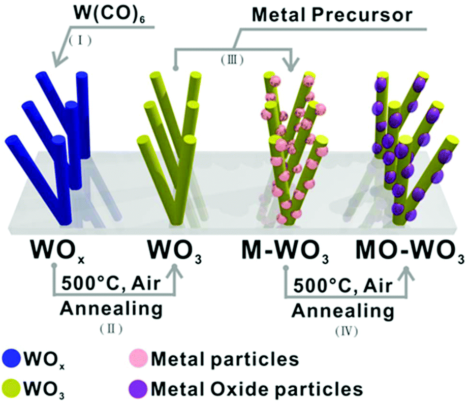 | ||
| Fig. 2 Schematic processes for fabrication of metal or metal oxide nanoparticles supported on a tungsten oxide nanorod array on quartz substrate via AACVD. | ||
| Sample | Precursor [g] | Solvent [mL] | Temperature [°C] | N2 flow rate [SCCM] |
|---|---|---|---|---|
| Au/WO3 | HAuCl4 [0.001] | Methanol [15] | 350 | 300 |
| Pd/WO3 | (NH4)2PdCl4 [0.001] | Methanol [15] | 350 | 300 |
| Ru/WO3 | Ru3(CO)12 [0.001] | Methanol [15] | 350 | 400 |
| Pt/WO3 | H2PtCl6 [0.001] | Methanol [15] | 350 | 300 |
Characterization
Scanning Electron Microscopy (SEM) images were obtained on a JEOL 6301F. Samples were coated with gold for 60 seconds and scanned at 5 kV. X-Ray diffraction (XRD) patterns were acquired by a Bruker D8-Discover reflection diffractometer equipped with a LinxEye silicon strip detector using Cu Kα radiation operated at 40 kV and 40 mA. The X-ray photoelectron (XPS) analysis was carried on a Thermo Scientific K-Alpha instrument equipped with a monochromatic Al Kα radiation (1486.6 eV) with charge compensation by a beam charge neutralization argon-ion gun (≤10 eV), and calibrated by the C 1s peak at 284.8 eV. Transmission electron microscopy (TEM) and scanning TEM (STEM) analysis was performed on a JEOL 2100 at 300 kV equipped with energy dispersion X-ray (EDX) detector (X-MaxN 80, Oxford Instruments).Photocatalytic activity tests
The as-synthesized WO3 thin films were dip-coated with a thin layer of stearic acid (SA) from a 0.05 M SA and chloroform solution, and then irradiated by a UVA bulb (Philips TL-D 18W BLB*4) (4.2 mW cm−2) in the range of 340 to 410 nm (maximum at 365 nm) with area of samples 0.78 cm2. The photodegradation of SA was monitored by a Fourier transform infrared (FTIR) spectrometer (PerkinElmer RX-1) in the range from 2700–3000 cm−1. To evaluate the activity of photodegradation of SA, the IR spectra were collected in absorbance mode and integrated the areas of typical peaks at 2958, 2923 and 2853 cm−1, representing for the C–H bonds of SA, changing give an estimation of the number of SA molecules degraded during irradiated by UV light using the conversion factor (1 cm−1 ≡ 9.7 × 10¹⁵ molecules) presented in the literature.473. Results and discussion
The WOx NR array thin films were grown directly on quartz via AACVD.42,48,49 Glancing angle X-ray diffraction (XRD) showed the as-synthesized WOx matched W32O84 (WO2.63) (PDF 77-0810, a = 21.43, b = 17.77, c = 3.79 Å, α = 90°, β = 90°, γ = 90°) with two strong peaks attributed to (001) and (002) reflections (Fig. 3a (blue line)). After annealing at 500 °C for 2 hours, the thin films turned from blue to white (Fig. S1†) and were characterised as monoclinic WO3 (m-WO3) (PDF 072-0677, a = 7.306, b = 7.540, c = 7.692 Å and α = 90°, β = 90.881°, γ = 90°) with a dominant (002) reflection (Fig. 3a (yellow line)). | ||
| Fig. 3 (a) Glancing angle XRD patterns of the WOx thin film deposited for 5 min on quartz by AACVD (blue line) matching the W32O84 (WO2.63) reference pattern (black colour) (PDF 77-0810, a = 21.43, b = 17.77, c = 3.79 Å, α = 90°, β = 90°, γ = 90°). After annealing at 500 °C in air for 2 hours, that pattern (yellow line) matches the monoclinic WO3 reference pattern (red colour) (PDF 072-0677, a = 7.306, b = 7.540, c = 7.692 Å and α = 90°, β = 90.881°, γ = 90°). SEM images of WO3 NR array thin film on top view (b) and cross-section (c) where A typical single NR (d) abstracted with 820 nm in length, grows along [001] direction with interplanar spacing 0.38 (±0.005) nm corresponding to (002) plane determined by HRTEM (e) and FFT of HRTEM image (inset). (f) W 4f region of WO3 NR arrays thin film (fitting peak in red, peak of W+6 in yellow, peak of W+4/+5 in blue). | ||
The as-synthesized WO3 thin films were approximately 1.0 ± 0.2 μm thick and comprised of arrays of NRs with random orientation, as shown by scanning electron microscopy (SEM) (Fig. 3b and c). A single NR about 820 nm in length was examined by transmission electron microscopy (TEM, Fig. 3d), showing interplanar spacing 0.38 (±0.005) nm corresponding to the (002) plane of m-WO3 (Fig. 3e). This is in good agreement with XRD which shows preferred orientation in (002) implying the growth of NRs along the [001] direction. The corresponding Fourier fast transformation (FFT) of the TEM image (Fig. 3e inset) indicates a streak perpendicular to the [001] direction which can be attributed to planar defects in [010] and/or [100] directions.42,48,49 XPS was used to identify the composition of the tungsten oxide NR arrays as shown in Fig. 3f. In the W 4f region, binding energy of 34.9 eV is assigned to W6+ (Fig. 3f in yellow colour) and 34.1 eV assigned to W4+/5+ (Fig. 3f in blue colour) suggested that the presence of oxygen deficient in surface.44
The metal NPs were deposited on the as-synthesized WO3 NR array, with the size controlled by the deposition time (0.5 to 36 min) during AACVD. The obtained metal NPs/WO3 NRs hybrid nanostructure thin films are denoted as M/WO3 (‘t’ minutes), where ‘t’ is the deposition time for the metal precursor during AACVD. The TEM images (Fig. 4), show the M/WO3 hybrid nanostructure, with the NPs homogenously dispersed on the WO3 NRs. For an Au/WO3 (1 min) sample the NPs have a mean size of approximately 3.0 nm and interplanar spacing of 0.23 and 0.20 (±0.01) nm corresponding to the (111) and (200) plane of Au metal (Fig. 4a) respectively. This correlates with X-ray photoelectron spectroscopy (XPS) spectra which confirm the presence of Au(0) with the Au 4f7/2 peak at 84.0 eV (Fig. 5a).50 The NPs of Pd/WO3 (5 min) have mean size around 1.9 nm and interplanar spacing 0.22 (±0.01) nm attributed to the (111) plane of Pd metal (Fig. 4b). XPS shows the presence of Pd(0) as well as Pd(II) (Fig. 5c), with Pd 3d5/2 peaks corresponding to Pd metal (335.8 eV) and PdCl2 (338.4 eV) respectively and the ratio of Pd:PdCl2 = 2.65:1 (details in Table S1†).51,52 The presence of PdCl2 is surprising, but may indicate incomplete decomposition of the precursor ((NH4)2PdCl4) in this instance. The NPs of Ru/WO3 (36 min) are comprised of both Ru(0) and Ru(IV), with Ru 3d5/2 peaks apparent for Ru metal (280.1 eV) and RuO2 (280.7 eV) respectively (Fig. 5d), with a ratio of Ru:RuO2 = 0.86:1 (details in Table S1†),53,54 and mean particle size around 2.8 nm. The interplanar spacing of 0.21 and 0.20 (±0.01) nm is attributed to the (002) and (101) plane of Ru metal (Fig. 4c) respectively. The NPs of Pt/WO3 (10 min), show only Pt(0) in the XPS spectra (Fig. 5b, Pt 4f7/2 at 71.2 eV),55 have mean particle size around 3.0 nm, with a particle interplanar spacing of 0.22 and 0.20 (±0.01) nm attributed to the (111) and (200) plane of Pt metal (Fig. 4d) respectively. The XRD patterns of all the M/WO3 thin films look similar to the undecorated WO3 NRs thin films (Fig. S2†) most likely due to the small amount and size of NPs, as described in previous literature.23 As deposition time increases during AACVD the metal NPs became larger (Table 2) with more extensive coverage of the surface of the WO3 NRs (Fig. S3–S6†). Hence the size and number concentration of metal NPs dispersing on WO3 NRs are able to be simply tailored by the deposition time during AACVD (Table 2).
 | ||
| Fig. 4 TEM images of M/WO3 or MO/WO3 hybrid nanostructure thin films: (a) Au/WO3 (1 min), (b) Pd/WO3 (5 min), (c) Ru/WO3 (36 min), (d) Pt/WO3 (10 min), (e) PdO/WO3 (5 min), (f) RuO2/WO3 (36 min) with metal or metal oxide NP size distributions on WO3 NR and inset zoom-in images of metal or metal oxide NP showing their predominantly exposed facet. | ||
 | ||
| Fig. 5 XPS spectra of the as-synthesized hybrid nanostructure thin films: (a) Au/WO3 (1 min), (b) Pt/WO3 (10 min), (c) Pd/WO3 (5 min), (d) Ru/WO3 (36 min), (e) PdO/WO3 (5 min), (f) RuO2/WO3 (36 min) (the peak in black at 284.8 eV is corresponding to carbon). | ||
| Sample | Depos. time [minute] | Meana [nm] | Std. dev. [nm] | Min [nm] | Max [nm] | Concentrationb [NPs per nm2] × 10−3 | Coveragec |
|---|---|---|---|---|---|---|---|
| a The mean particle size is obtained by counting NPs (>200 particles) from many different WO3 NRs in TEM images. b The number concentration of NPs is estimated by counting the number of NPs on a WO3 NR and then divided by the surface area of that NR. c The coverage of NPs on a WO3 NR surface estimated by the equation [nπ(0.5d)2]/(0.5S) where n is the number concentration, d is the mean size of NPs and S is the surface area of that NR calculated by 2πrl (r and l is the diameter and length of NR obtained by measures from TEM images). | |||||||
| Au/WO3 | 0.5 | 2.4 | 0.5 | 1.5 | 5.2 | 1.29 | 0.6% |
| 1 | 3.0 | 0.6 | 1.7 | 5.0 | 5.23 | 3.7% | |
| 5 | 5.5 | 1.3 | 2.8 | 9.9 | 1.62 | 3.9% | |
| 10 | 6.1 | 1.2 | 3.6 | 10.2 | 1.74 | 5.1% | |
| 20 | 6.8 | 1.4 | 4.3 | 11.1 | 2.46 | 8.8% | |
| 35 | 7.3 | 1.8 | 5.0 | 14.7 | 3.61 | 15.1% | |
| Pd/WO3 | 5 | 1.9 | 0.4 | 0.8 | 3.0 | 3.54 | 1.0% |
| 10 | 1.9 | 0.4 | 0.9 | 3.4 | 4.32 | 1.2% | |
| 20 | 3.4 | 0.8 | 1.7 | 5.9 | 7.14 | 6.6% | |
| 35 | 4.1 | 0.7 | 2.1 | 5.7 | 11.12 | 14.3% | |
| Pt/WO3 | 1 | — | — | — | Trace | — | |
| 5 | 3.0 | 1.0 | 1.2 | 6.1 | 0.85 | 0.6% | |
| 10 | 3.0 | 1.0 | 1.4 | 6.5 | 3.69 | 2.6% | |
| 20 | 7.1 | 1.7 | 2.8 | 12.9 | 1.85 | 7.3% | |
| Ru/WO3 | 1 | 1.6 | 0.6 | 0.7 | 3.6 | 3.54 | 0.7% |
| 10 | 2.2 | 0.7 | 0.5 | 4.9 | 11.91 | 4.6% | |
| 20 | 2.3 | 0.5 | 1.1 | 3.9 | 11.96 | 5.1% | |
| 36 | 2.9 | 0.7 | 0.9 | 5.7 | 10.83 | 6.5% | |
| PdO/WO3 | 1 | — | — | — | Trace | — | |
| 5 | 5.6 | 1.5 | 3.2 | 10.0 | 0.56 | 1.4% | |
| 10 | 5.3 | 1.2 | 2.9 | 7.4 | 2.92 | 6.5% | |
| 20 | 5.5 | 0.9 | 3.7 | 9.8 | 3.76 | 9.0% | |
| 35 | 6.5 | 1.6 | 3.3 | 13.7 | 3.85 | 12.8% | |
| RuO2/WO3 | 1 | 3.7 | 1.0 | 2.2 | 7.1 | 2.36 | 2.5% |
| 5 | 4.8 | 1.0 | 2.7 | 7.9 | 6.11 | 11.2% | |
| 10 | 5.1 | 1.2 | 2.5 | 8.9 | 6.28 | 12.8% | |
| 20 | 4.8 | 1.2 | 1.7 | 8.4 | 6.97 | 12.7% | |
| 36 | 5.1 | 1.1 | 2.4 | 9.4 | 6.44 | 13.2% | |
An oxidative treatment (e.g. annealing) is able to oxidise some metal NPs on the WO3 NRs to give in situ formation of metal oxide/WO3 hybrid nanostructures denoted as MO/WO3 (Fig. S7 and S8†). The Pd/WO3 (5 min) and Ru/WO3 (36 min) were annealed at 500 °C in air for 2 hours to produce PdO/WO3 (5 min) and RuO2/WO3 (36 min). Both samples have NPs with larger particle mean size, 5.6 and 5.1 nm respectively compared to counterparts before annealing, due to particle oxidation and/or coalescence (Fig. 4e and f). The oxidative processes were confirmed by their XPS spectra which show the NPs of PdO/WO3 (5 min) contain PdO with the Pd 3d5/2 peak shifting to higher binding energy, matching reference PdO (337.2 eV) (Fig. 5e),56 and the NPs of RuO2/WO3 (36 min) containing not just Ru(IV) but also Ru(VI), with the Ru 3d5/2 peaks shifting to higher binding energy matching the reference values for RuO2 (280.8 eV) and RuO3 (282.5 eV) respectively (Fig. 5f), with a ratio of RuO2:RuO3 = 0.67:1 (details in Table S1†).57,58 The metal oxide NPs could not be observed by XRD (Fig. S2†) likely due to a similar explanation as for M/WO3. The NPs of PdO/WO3 (5 min) and RuO2/WO3 (36 min) have interplanar spacing of 0.27 and 0.21 (±0.01) nm and 0.22 (±0.01) nm attributed to the (002) and (110) plane of PdO and the (200) plane of RuO2 respectively (Fig. 4e and f inset).
The effect of modifying WO3 NRs to form M/WO3 and MO/WO3 1D hybrid nano-heterostructured thin films was evaluated by photo-degradation of stearic acid (SA). The photodegradation rate of SA under UVA irradiation (365 nm and 4.2 mW cm−2) is reported as formal quantum efficiency (FQE), defined as the amount of SA molecules photodegraded per incident photon estimated by linear regression of the initial 30 to 40% steps (Fig. 6a and b). The sample Au/WO3 (1 min, with particle mean size 3.0 nm) and sample Pt/WO3 (10 min, 3.0 nm) showed enhanced activity for photocatalytic degradation of SA with FQE = 11.0 × 10⁻⁵ and 11.3 × 10⁻⁵ respectively compared to an undecorated WO3 NR array thin film (deposition time of 5 minutes, FQE = 8.7 × 10⁻⁵ which was the best photocatalytic activity for WO3 NRs array thin films according to our previous study).44 Whereas, when the WO3 NR array was functionalised by Pd and Ru NPs (sample Pd/WO3 (5 min, 1.9 nm) and Ru/WO3 (36 min, 2.8 nm)) a lower activity for photocatalytic degradation of SA was observed. After annealing, the sample PdO/WO3 (5 min, 5.6 nm) had the highest activity for photocatalytic degradation of SA with FQE = 13.2 × 10⁻⁵, though RuO2/WO3 (36 min, 5.1 nm) still showed lower activity (FQE = 6.0 × 10⁻⁵).
 | ||
| Fig. 6 Integrated areas of stearic acid bands (a) were estimated during UVA light (4.2 mW cm−2) irradiation of SA coated as-synthesized M/WO3 and MO/WO3 hybrid nanostructure thin films: (1) plain WO3 NR array, (2) Au/WO3 (1 min), (3) Pd/WO3 (5 min), (4) Ru/WO3 (36 min), (5) Pt/WO3 (10 min), (6) PdO/WO3 (5 min), (7) RuO2/WO3 (36 min). Formal quantum efficiencies (b), given as degraded SA molecules by per incident photon in unit (molecule per photon), were calculated from the initial rates of photodegradation of SA (a). Illustration of the possible band alignment (c) of noble metal (Au/Pt) or PdO NPs/WO3 NRs hybrid nanostructure, and the mechanism of electron–hole separation of those samples activating general reactions for the photocatalytic degradation of organic pollutant: (I) the reduction reaction of O2 producing superoxide radicals (O2˙) and/or hydroperoxy radical (HO2˙), (II) the oxidation reaction of H2O creating hydroxyl radical (OH˙) based on the previous literatures.59,61–64 | ||
The degradation of SA generally involves two photoreactions: (I) the intermediate hydroxyl (˙OH) radicals which are generated by photo-oxidising H2O, and (II) the hydroperoxy (HO2˙) radicals which are generated by photo-reducing O2.59 Photocatalytic degradation of organic pollutants can proceed indefinitely when both of these radicals are able to participate in the degradation reaction.60 The valence band maximum (VBM) potential of WO3 is sufficiently positive (vs. NHE) to photo-oxidise H2O to ˙OH, but the conduction band minimum (CBM) potential is insufficiently negative (vs. NHE) to photo-reduce O2 to HO2˙, and as a result bulk WO3 is inactive for photodegradation of SA.59,61 To understand whether M/WO3 or MO/WO3 hybrid structures could enhance the activity of photodegradation of SA, the band alignment was estimated as shown in Fig. 6c, in agreement with previous reports.59,61–64 The indirect bandgap and VBM of as-synthesized WO3 NR array thin films (5 min deposition) were obtained by Tauc plots (3.0 eV) and XPS valence band scans (2.7 eV, with respect to the Fermi level = 0 eV) (Fig. S9†). All the VBM of M and MO NPs, obtained from pure M and MO NP thin films, were located around or below the Fermi level (0 eV) (Fig. S10†), and elevate VBM of the counterpart 1D hybrid material thin films compared to as-synthesized WO3 NR array thin films (5 min deposition) (Fig. S11†). Consequently Au and Pt NPs are expected to accept photogenerated electrons from WO3 NR, in agreement with previous reports that Au NPs with particle size below 3 nm are reported to be catalytically active for the partial oxidation of styrene by dissociation of chemisorbed O2 to produce O adatoms,22 and that Pt NPs with particle size below 5 nm can act as a catalyst for promoting O2 reduction into H2O2 and superoxide radicals.65 The PdO NP can also act as an electron acceptor, reducing O2 and producing HO2˙ radicals.63 In addition PdO is an expected p-type semiconductor and hence forms a p–n junction with WO3 (an expected n-type semiconductor), which is expected to promote electron–hole separation and production of HO2˙ radicals.66 The sample Pd/WO3 (5 min, 1.9 nm) showed lower activity of photocatalytic degradation of SA than unmodified WO3 which contradicts previous literature that TiO2 supported Pd NPs showed enhanced photocatalysis,67 which may be attributable to the PdCl2 found by XPS in the Pd metal NPs. The reason for the low activity of the Ru/WO3 (36 min, 2.8 nm) and RuO2/WO3 (36 min, 5.1 nm) samples is unclear, but possibly relates to Ru and RuO2 NPs having known activity as catalysts for O2 evolution,68,69 as opposed to Au, Pt and PdO NPs which are known for O2 reduction. However, the fully understand of their photoactivity is still unclear, more factors need to be considered such as the local surface plasmon resonances (LSPR) of noble metal and their oxide NPs on WO3 NRs appearing strong absorption peaks in optical spectra as shown in Fig. S1† (peaks at around 500 nm or 1000 nm corresponding to the colour change of 1D hybrid thin films) increase the light absorption in visible and/or NIR range, also need to take account of the size, distribution and coverage of noble metal or their oxide NPs on WO3 NRs and metal NP-NR support interaction, etc.
4. Conclusion
We have demonstrated that a two-step AACVD deposition process is a versatile tool to fabricate metal (M) and metal oxide (MO) nanoparticles (NPs)/WO3 nanorod (NR) hybrid thin films which requires no additional agents or catalysts, with the M/MO particle size tuned simply by altering the deposition time. In the demonstration here it was possible to optimise the photocatalytic properties, for example for Au NPs a mean particle size of 3.0 nm (deposited by 1 min via AACVD on WO3 NRs) showed the best performance for photodegradation of SA, being around three times more active than that for Au NPs with mean size 6.8 nm (deposted by 20 min AACVD on WO3 NRs, Fig. S12†). This method is suitable for constructing different types of hybrid thin films by depositing a wide range of metal and metal oxide NPs (or quantum dots and nanocrystals) on various thin film supports fabricated by different methods (e.g. Au NPs on flat TiO2 support by APCVD70,71), and also for developing simple scalable routes to heterojunctions for application in gas sensing, photovoltaic, photocatalysis, catalysis and surface enhanced Raman spectroscopy. Our future aim is to combine this process with other techniques to fabricate various types of hybrid nano-heterostructured thin films based on wide range of 1D substrates e.g. ZnO,72 SnO2,73 MgO,74 In2O3,75 Ga2O3,76 TiO2,77 W2N38etc.
Conflicts of interest
There are no conflicts to declare.Acknowledgements
Dr Steven Firth, Dr Dr Kevin Reeves and Dr Tom Gregory are thanked for SEM and TEM training.References
- K. J. Choi and H. W. Jang, Sensors, 2010, 10, 4083–4099 CrossRef CAS PubMed.
- M. J. S. Spencer, Prog. Mater. Sci., 2012, 57, 437–486 CrossRef CAS.
- Q. Zhang and G. Cao, Nano Today, 2011, 6, 91–109 CrossRef CAS.
- M. Yu, Y.-Z. Long, B. Sun and Z. Fan, Nanoscale, 2012, 4, 2783–2796 RSC.
- Y. Xia, P. Yang, Y. Sun, Y. Wu, B. Mayers, B. Gates, Y. Yin, F. Kim and H. Yan, Adv. Mater., 2003, 15, 353–389 CrossRef CAS.
- Z. Fan, R. Kapadia, P. W. Leu, X. Zhang, Y.-L. Chueh, K. Takei, K. Yu, A. Jamshidi, A. A. Rathore, D. J. Ruebusch, M. Wu and A. Javey, Nano Lett., 2010, 10, 3823–3827 CrossRef CAS PubMed.
- Z. Fan, H. Razavi, J. Do, A. Moriwaki, O. Ergen, Y.-L. Chueh, P. W. Leu, J. C. Ho, T. Takahashi, L. A. Reichertz, S. Neale, K. Yu, M. Wu, J. W. Ager and A. Javey, Nat. Mater., 2009, 8, 648–653 CrossRef CAS PubMed.
- A. I. Hochbaum and P. Yang, Chem. Rev., 2010, 110, 527–546 CrossRef CAS PubMed.
- M. A. Green and S. R. Wenham, Appl. Phys. Lett., 1994, 65, 2907 CrossRef CAS.
- E. Comini, C. Baratto, G. Faglia, M. Ferroni, A. Vomiero and G. Sberveglieri, Prog. Mater. Sci., 2009, 54, 1–67 CrossRef CAS.
- J. G. Lu, P. Chang and Z. Fan, Mater. Sci. Eng., R, 2006, 52, 49–91 CrossRef.
- B. Hvolbæk, T. V. W. Janssens, B. S. Clausen, H. Falsig, C. H. Christensen and J. K. Nørskov, Nano Today, 2007, 2, 14–18 CrossRef.
- O. M. Wilson, M. R. Knecht, J. C. Garcia-Martinez and R. M. Crooks, J. Am. Chem. Soc., 2006, 128, 4510–4511 CrossRef CAS PubMed.
- S. H. Joo, J. Y. Park, J. R. Renzas, D. R. Butcher, W. Huang and G. A. Somorjai, Nano Lett., 2010, 10, 2709–2713 CrossRef CAS PubMed.
- R. Jiang, B. Li, C. Fang and J. Wang, Adv. Mater., 2014, 26, 5274–5309 CrossRef CAS PubMed.
- R. V. Hull, L. Li, Y. Xing and C. C. Chusuei, Chem. Mater., 2006, 18, 1780–1788 CrossRef CAS.
- J. Sunarso, A. M. Glushenkov, A. A. J. Torriero, P. C. Howlett, Y. Chen, D. R. MacFarlane and M. Forsyth, J. Electrochem. Soc., 2012, 160, H74–H79 CrossRef.
- R. Jiang, B. Li, C. Fang and J. Wang, Adv. Mater., 2014, 26(31), 5274–5309 CrossRef CAS PubMed.
- S. J. Tauster, S. C. Fung, R. T. Baker and J. A. Horsley, Science, 1981, 211, 1121–1125 CrossRef CAS PubMed.
- G. N. Vayssilov, Y. Lykhach, A. Migani, T. Staudt, G. P. Petrova, N. Tsud, T. Skála, A. Bruix, F. Illas, K. C. Prince, V. Matolín, K. M. Neyman and J. Libuda, Nat. Mater., 2011, 10, 310–315 CrossRef CAS PubMed.
- M. Haruta, Catal. Today, 1997, 36, 153–166 CrossRef CAS.
- M. Turner, V. B. Golovko, O. P. H. Vaughan, P. Abdulkin, A. Berenguer-Murcia, M. S. Tikhov, B. F. G. Johnson and R. M. Lambert, Nature, 2008, 454, 981–983 CrossRef CAS PubMed.
- G. Xi, J. Ye, Q. Ma, N. Su, H. Bai and C. Wang, J. Am. Chem. Soc., 2012, 134, 6508–6511 CrossRef CAS PubMed.
- W. Li, R. Xu, M. Ling and G. He, Opt. Mater., 2017, 72, 529–532 CrossRef CAS.
- S. Vallejos, P. Umek, T. Stoycheva, F. Annanouch, E. Llobet, X. Correig, P. De Marco, C. Bittencourt and C. Blackman, Adv. Funct. Mater., 2013, 23, 1313–1322 CrossRef CAS.
- F. Di Maggio, M. Ling, A. Tsang, J. Covington, J. Saffell and C. Blackman, J. Sens. Sens. Syst., 2014, 3(2), 325–330 CrossRef.
- F. E. Annanouch, Z. Haddi, M. Ling, F. Di Maggio, S. Vallejos, T. Vilic, Y. Zhu, T. Shujah, P. Umek, C. Bittencourt, C. Blackman and E. Llobet, ACS Appl. Mater. Interfaces, 2016, 8, 10413–10421 CrossRef CAS PubMed.
- P. Mao, F. Sun, H. Yao, J. Chen, B. Zhao, B. Xie, M. Han and G. Wang, Nanoscale, 2014, 6, 8177–8184 RSC.
- P. Mao, A. Krishna Mahapatra, J. Chen, M. Chen, G. Wang and M. Han, ACS Appl. Mater. Interfaces, 2015, 7, 19179–19188 CrossRef CAS PubMed.
- K. C. Poon, D. C. L. Tan, T. D. T. Vo, B. Khezri, H. Su, R. D. Webster and H. Sato, J. Am. Chem. Soc., 2014, 136, 5217–5220 CrossRef CAS PubMed.
- F. Kruis, H. Fissan and A. Peled, J. Aerosol Sci., 1998, 29, 511–535 CrossRef CAS.
- K. Choy, Prog. Mater. Sci., 2003, 48, 57–170 CrossRef CAS.
- R. Cai, P. R. Ellis, J. Yin, J. Liu, C. M. Brown, R. Griffin, G. Chang, D. Yang, J. Ren, K. Cooke, P. T. Bishop, W. Theis and R. E. Palmer, Small, 2018, 14, 1703734 CrossRef PubMed.
- S. Vallejos, T. Stoycheva, P. Umek, C. Navio, R. Snyders, C. Bittencourt, E. Llobet, C. Blackman, S. Moniz and X. Correig, Chem. Commun., 2011, 47, 565–567 RSC.
- F. E. Annanouch, Z. Haddi, S. Vallejos, P. Umek, P. Guttmann, C. Bittencourt and E. Llobet, ACS Appl. Mater. Interfaces, 2015, 7, 6842–6851 CrossRef CAS PubMed.
- S. Vallejos, I. Gràcia, E. Figueras and C. Cané, ACS Appl. Mater. Interfaces, 2015, 7, 18638–18649 CrossRef CAS PubMed.
- C. Sotelo-Vazquez, R. Quesada-Cabrera, M. Ling, D. O. Scanlon, A. Kafizas, P. K. Thakur, T.-L. Lee, A. Taylor, G. W. Watson, R. G. Palgrave, J. R. Durrant, C. S. Blackman and I. P. Parkin, Adv. Funct. Mater., 2017, 27, 1605413 CrossRef.
- G. He, M. Ling, X. Han, D. I. Abou El Amaiem, Y. Shao, Y. Li, W. Li, S. Ji, B. Li, Y. Lu, R. Zou, F. Ryan Wang, D. J. L. Brett, Z. Xiao Guo, C. Blackman and I. P. Parkin, Energy Storage Mater., 2017, 9, 119–125 CrossRef.
- K. S. Ranjith and R. T. Rajendra Kumar, Nanotechnology, 2016, 27, 095304 CrossRef CAS PubMed.
- G.-H. Nam, S.-H. Baek, C.-H. Cho and I.-K. Park, Nanoscale, 2014, 6, 11653–11658 RSC.
- P. Marchand, I. A. Hassan, I. P. Parkin and C. J. Carmalt, Dalton Trans., 2013, 42, 9406–9422 RSC.
- M. Ling and C. Blackman, Phys. Status Solidi, 2015, 12, 869–877 CrossRef CAS.
- S. Ashraf, C. S. Blackman, R. G. Palgrave, S. C. Naisbitt and I. P. Parkin, J. Mater. Chem., 2007, 17, 3708–3713 RSC.
- M. Ling, C. S. Blackman, R. G. Palgrave, C. Sotelo-Vazquez, A. Kafizas and I. P. Parkin, Adv. Mater. Interfaces, 2017, 4, 1700064 CrossRef.
- A. Kafizas, L. Francàs, C. Sotelo-Vazquez, M. Ling, Y. Li, E. Glover, L. McCafferty, C. Blackman, J. Darr and I. Parkin, J. Phys. Chem. C, 2017, 121, 5983–5993 CrossRef CAS.
- D. Tsukamoto, Y. Shiraishi, Y. Sugano, S. Ichikawa, S. Tanaka and T. Hirai, J. Am. Chem. Soc., 2012, 134, 6309–6315 CrossRef CAS PubMed.
- A. Mills and J. Wang, J. Photochem. Photobiol., A, 2006, 182, 181–186 CrossRef CAS.
- J. Zhou, Y. Ding, S. Z. Deng, L. Gong, N. S. Xu and Z. L. Wang, Adv. Mater., 2005, 17, 2107–2110 CrossRef CAS.
- A. M. Smith, M. G. Kast, B. A. Nail, S. Aloni and S. W. Boettcher, J. Mater. Chem. A, 2014, 2, 6121–6129 RSC.
- M. P. Seah, G. C. Smith and M. T. Anthony, Surf. Interface Anal., 1990, 15, 293–308 CrossRef CAS.
- A. Tressaud, S. Khairoun, H. Touhara and N. Watanabe, Z. Anorg. Allg. Chem., 1986, 540, 291–299 CrossRef.
- M. C. Militello, Surf. Sci. Spectra, 1994, 3, 402 CrossRef CAS.
- J. Hrbek, J. Vac. Sci. Technol., A, 1986, 4, 86 CrossRef CAS.
- C. S. Huang, M. Houalla, D. M. Hercules, C. L. Kibby and L. Petrakis, J. Phys. Chem., 1989, 93, 4540–4544 CrossRef CAS.
- C. D. Wagner, Faraday Discuss. Chem. Soc., 1975, 60, 291 RSC.
- M. C. Militello, Surf. Sci. Spectra, 1994, 3, 395 CrossRef CAS.
- J. Y. Shen, A. Adnot and S. Kaliaguine, Appl. Surf. Sci., 1991, 51, 47–60 CrossRef CAS.
- D. D. Sarma and C. N. R. Rao, J. Electron Spectrosc. Relat. Phenom., 1980, 20, 25–45 CrossRef CAS.
- A. Mills, R. H. Davies and D. Worsley, Chem. Soc. Rev., 1993, 22, 417 RSC.
- B. Ohtani, Chem. Lett., 2008, 37, 216–229 CrossRef.
- A. Kudo and Y. Miseki, Chem. Soc. Rev., 2009, 38, 253–278 RSC.
- A. Mills and S. Le Hunte, J. Photochem. Photobiol., A, 1997, 108, 1–35 CrossRef CAS.
- W. Zhou, Y. Guan, D. Wang and X. Zhang, Chem. – Asian J., 2014, 9, 1648–1654 CrossRef CAS PubMed.
- N. Zhou, V. López-Puente, Q. Wang, L. Polavarapu, I. Pastoriza-Santos and Q.-H. Xu, RSC Adv., 2015, 5, 29076–29097 RSC.
- R. Abe, H. Takami, N. Murakami and B. Ohtani, J. Am. Chem. Soc., 2008, 130, 7780–7781 CrossRef CAS PubMed.
- P. O. Nilsson, J. Phys. C: Solid State Phys., 1979, 12, 1423–1427 CrossRef CAS.
- A. M. Lacerda, I. Larrosa and S. Dunn, Nanoscale, 2015, 7, 12331–12335 RSC.
- T. Ohno, F. Tanigawa, K. Fujihara, S. Izumi and M. Matsumura, J. Photochem. Photobiol., A, 1999, 127, 107–110 CrossRef CAS.
- K. Teramura, K. Maeda, T. Saito, T. Takata, N. Saito, Y. Inoue and K. Domen, J. Phys. Chem. B, 2005, 109, 21915–21921 CrossRef CAS PubMed.
- A. Kafizas, X. Wang, S. R. Pendlebury, P. Barnes, M. Ling, C. Sotelo-Vazquez, R. Quesada-Cabrera, C. Li, I. P. Parkin and J. R. Durrant, J. Phys. Chem. A, 2016, 120, 715–723 CrossRef CAS PubMed.
- A. Kafizas, Y. Ma, E. Pastor, S. R. Pendlebury, C. Mesa, L. Francàs, F. Le Formal, N. Noor, M. Ling, C. Sotelo-Vazquez, C. J. Carmalt, I. P. Parkin and J. R. Durrant, ACS Catal., 2017, 7, 4896–4903 CrossRef CAS.
- S. Vallejos, N. Pizúrová, I. Gràcia, C. Sotelo-Vazquez, J. Čechal, C. Blackman, I. Parkin and C. Cané, ACS Appl. Mater. Interfaces, 2016, 8, 33335–33342 CrossRef CAS PubMed.
- S. Vallejos, S. Selina, F. E. Annanouch, I. Gràcia, E. Llobet and C. Blackman, Sci. Rep., 2016, 6, 28464 CrossRef PubMed.
- A. G. Nasibulin, L. Sun, S. Hämäläinen, S. D. Shandakov, F. Banhart and E. I. Kauppinen, Cryst. Growth Des., 2010, 10, 414–417 CrossRef CAS.
- J. Q. Xu, et al. , Nanotechnology, 2007, 18, 115615 CrossRef.
- W. Han, P. Kohler-Redlich, F. Ernst and M. Rühle, Solid State Commun., 2000, 115, 527–529 CrossRef CAS.
- Y. Wang, L. Zhang, K. Deng, X. Chen and Z. Zou, J. Phys. Chem. C, 2007, 111, 2709–2714 CrossRef CAS.
Footnote |
| † Electronic supplementary information (ESI) available. See DOI: 10.1039/c8nr06257a |
| This journal is © The Royal Society of Chemistry 2018 |