Remote homoepitaxy of ZnO microrods across graphene layers†
Abstract
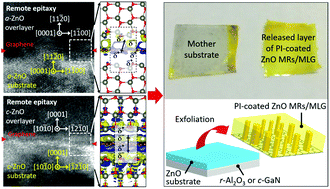
Two-dimensional atomic layered materials (2d-ALMs) are emerging candidates for use as epitaxial seed substrates for transferrable epilayers. However, the micrometer-sized domains of 2d-ALMs preclude their practical use in epitaxy because they cause crystallographically in-plane disordering of the overlayer. Ultrathin graphene can penetrate the electric dipole momentum from an underlying crystal layer to the graphene surface, which then drives it to crystallize the overlayer during the initial growth stage, thus resulting in substantial energy saving. This study demonstrates the remote homoepitaxy of ZnO microrods (MRs) on ZnO substrates across graphene layers via a hydrothermal method. Despite the presence of poly-domain graphene in between the ZnO substrate and ZnO MRs, the MRs were epitaxially grown on a- and c-plane ZnO substrates, whose in-plane alignments were homogeneous within the wafer's size. Transmission electron microscopy revealed a homoepitaxial relationship between the overlayer MRs and the substrate. Density-functional theory calculations suggested that the charge redistribution occurring near graphene induces the electric dipole formation, so the attracted adatoms led to the formation of the remote homoepitaxial overlayer. Due to a strong potential field caused by long-range charge transfer given from the substrate, even the use of bi-layer and tri-layer graphene resulted in remote homoepitaxial ZnO MRs. The effects of substrate crystal planes were also theoretically and empirically investigated. The ability of graphene, which can be released from the mother substrate without covalent bonds, was utilized to transfer the overlayer MR arrays. This method opens a way for producing well aligned, transferrable epitaxial nano/microstructure arrays while regenerating the substrate for cost-saving device manufacturing.


 Please wait while we load your content...