
 Open Access Article
 This Open Access Article is licensed under a
 Creative Commons Attribution 3.0 Unported Licence
Femtosecond transmission electron microscopy for nanoscale photonics: a numerical study†
C. W.
Barlow Myers
,
N. J.
Pine
and
W. A.
Bryan
 *
*
Department of Physics, College of Science, Swansea University, Singleton Park, Swansea SA2 8PP, UK. E-mail: w.a.bryan@swansea.ac.uk
First published on 2nd November 2018
Abstract
Recent developments in ultrafast electron microscopy have shown that spatial and temporal information can be collected simultaneously on very small and fast scales. In the present work, an instrumental design study with application to nanoscale dynamics, we optimize the conditions for a femtosecond transmission electron microscope (fs-TEM). The fs-TEM numerically studied employs a metallic nanotip source, electrostatic acceleration, magnetic lenses, a condenser-objective around the sample and a temporal compressor, and considers space-charge effects during propagation. We find a spatial resolution of the order of 1 nm and a temporal resolution of below 10 fs will be feasible for pulses comprised of on average 20 electrons. The influence of a transverse electric field at the sample plane is modelled, indicating 1 V μm−1 can be resolved, corresponding to a surface charge density of 10e per μm2, comparable to fields generated in light-driven electronics and ultrafast nanoplasmonics. The realisation of such an instrument is anticipated to facilitate unprecedented elucidation of laser-initiated physical, chemical and biological structural dynamics on atomic time- and length-scales.
1. Introduction
A grand challenge of condensed matter and nanoscale physics is to directly image the time evolution of ultrafast (picosecond to femtosecond) processes. Achieving such an unprecedented spatial and temporal resolution is demanding due to the characteristic small length and time scales over which these dynamics occur.1–5 Nonetheless, this is a worthwhile pursuit as it will facilitate access to the mapping of energy transport through lattice motions, understanding the dynamics of photon-initiated chemical reactions, the control of exciton and plasmon dynamics in quantum systems with light, and by extension, the dynamics of mesoscopic and macroscopic materials.Direct ultrafast imaging is achievable with a probe of sufficient brightness and short wavelength: electron matter waves meet these requirements. The simplest time resolved imaging with electrons has been achieved through lensless point-projection microscopy,6–10 carried out with sub-keV electrons generated from a nanoscale metal tip (NSMT).11–22 The penetration depth of such electrons is essentially zero (shadowgrams are formed), however are extremely sensitive to localised electromagnetic fields. Despite the distance between the NSMT and sample being of the order of hundreds of microns, the low accelerating field means the flight time is long, so these pulses are heavily distorted by space charge effects, and are often carried out with one electron per pulse.10 At the other extreme of the electron energy scale, relativistic (MeV) electron sources23–25 can deliver of the order of 106 electrons in a laser triggered bunch, facilitating single shot imaging.
Between these limits, femtosecond transmission electron microscopy (fs-TEM) has emerged as a very powerful tool with which to investigate nanoscale dynamics,26–41 impacting biology, medicine, chemistry, physics and engineering. The typical operating energy of fs-TEM (tens to hundreds of keV) allows penetration through thin samples, and naturally inherits mature electron optic and detector technologies from static TEM, along with powerful theoretical tools. From pioneering26–30 to more recent31–41 works, the balance between pulse charge, duration and energy is being explored, with optimization of microscope components and operating parameters to find a balance between spatial and temporal resolutions.
Recently, temporal and spatial manipulation of electron pulses by terahertz (THz),42–44 IR45–47 and radio-frequency (RF)48,49 photons have been demonstrated, along with novel characterization methods. These active compression methods can reverse the temporal stretch caused by space charge in multi-electron pulses,42–44,48 and transform a picosecond electron pulse to a train of attosecond electron bunches,45,46 giving access to ever-decreasing time-scales.
In this paper we present the numerical modelling and optimization of a novel femtosecond transmission electron microscope (fs-TEM) architecture, consisting of a NSMT photoelectron source, electron optics, and spatially resolved detection. Temporal dispersion is compensated, and studies of each beamline component are presented in the context of the preservation of pulse duration while maintaining as high an electron flux as possible. A magnetic condenser objective lens gives full control of the beam diameter and ensures that the angular velocity of the pulse is eliminated in the plane of the sample, with magnifications in excess of 105 possible. Images at the detector plane infer minimal spatial distortion. The minimum resolvable electric field in the vicinity of a nanoscale structure is examined, with a view to highlight applications in ultrafast nanophotonics and nanoplasmonics.
2. Methods
2.1 Numerical methods
To model the electrostatic landscape around the NSMT electron source we utilise Poisson Superfish.50 The length scales involved in our model, from nanometres to fractions of a metre, necessitates a variable mesh resolution when the geometry is discretized. To avoid discontinuities in the field maps the maximum change in mesh density between adjacent regions was limited to a factor of two. The numerical accuracy of Poisson was set to 10−10.The General Particle Tracer (GPT)51 is used for dynamic simulations, which employs macroparticles to represent the electron pulse, whereby the number of macroparticles and total pulse charge can be varied independently. 250 macroparticles were used for all simulations unless otherwise stated. The relativistic equations of motion of the individual macroparticles are solved by GPT in the time domain, utilising an embedded fifth-order Runge–Kutta algorithm with a variable step-size. GPT numerically calculates electron pulse trajectories through the acceleration region described by the Poisson Superfish field maps, mutual space charge, and the electric and magnetic fields generated by subsequent beamline components. Convergence tests on the accuracy and number of macroparticles were conducted, yielding sufficient accuracy while minimizing computational cost, with the accuracy for the numerical propagation is set to 10−8. Space charge is computed from 3D point-to-point relativistic particle–particle interactions, and included a test of representing a single electron as a 250 macroparticle collection of fractional charges. Clearly a single electron cannot experience space charge repulsion, however we verified that the predicted pulse characteristics were within the limits established by a “no space charge” case and two electrons. Furthermore, as will be seen, in this work we concern ourselves with many-electron pulses.
Optimization of GPT conditions (e.g. magnetic lens currents, oscillating electric field phase and amplitude, fs-TEM element positions) is manually tuned to find constraints, then the GPT “GDFsolve” root finder and optimizer routine finds the ideal conditions for a particular configuration. This method makes the best use of intuitive interaction with finding robust and convergent numerical solutions.
2.2 Design criteria
The numerically model is designed to satisfy the following conditions, which are derived from the type of applications envisaged, i.e. nanoscale photonics with short time and length scales. Optimization of each fs-TEM element, as described later, is then performed to balance and maximise the manner in which these conditions are met.(1) The spatial resolution of the instrument should be sufficient to resolve nanostructures. State of the art directly or fibre coupled TEM detectors have pixel sizes from five to tens of microns, and from 2k × 2k to 8k × 8k pixels over a sensor of up to 50 mm square. Taking a detector performance of 5 micron pixels and 8192 × 8192 pixels, a beam diameter at the sample of 6 microns would map a single pixel to 0.7 nm in the sample plane.
(2) To resolve nanophotonic electronic processes requires a single pulse temporal resolution of below 10 fs, i.e. not a pulse train. This will take the performance of the modelled instrument beyond what is currently possible. Utilising a single drive laser system to trigger photoemission, temporal compression and the optical pump of the sample should ensure a jitter down to single femtoseconds.40 This is on the condition that the THz radiation parameters are entirely reproducible; in practice uncertainties must be considered that will degrade spatial and temporal resolutions.
(3) Delivering as many electrons per pulse as possible is advantageous but requires care. A 70 keV TEM with a 10 nA beam spatially focussed to a spot of radius 1 μm corresponds to 1015 e m−3. A 10 fs electron pulse of the same energy and a 0.5 eV bandwidth containing 10 electrons generates densities of 1019e per m3, so the mitigation of this factor is vital.
(4) All electrons emitted from the NSMT should contribute to image formation. Employing apertures would improve both the spatial (smaller convergence angles) and temporal (minimizing geometric effects) resolution, but, as shown later, an electron pulse of hundreds of electrons can stretch to hundreds of femtoseconds. The stretch of a very high flux pulse which is highly apertured in the first few millimetres makes the requirement of the compressor more significant.
2.3 Magnetic lenses
Any fs-TEM architecture requires lenses to transport the electron pulse from the source to sample then to the detector. Magnetic rather than electrostatic lenses are used in TEM due to an improved optical performance and lack of requirement for high voltages. In our modelled instrument, all lenses are single loop solenoids, allowing GPT to calculate magnetic fields analytically rather than using the Poisson solver. This is advantageous as single loop solenoids are computationally efficient and require no approximations. On the other hand, employing a single loop solenoids to describe the extended field of a magnetic lens with pole-pieces is very limited in the manner in which it represents fringing fields. We note therefore that a more complete treatment will be required before a practical manufacturing design is finalized, and that such fringe effects are likely to induce multi-order aberrations which will have a detrimental influence on the spatial resolution.To ensure the single loops employed are a fair analogue to physically achievable lenses, we require that the fields generated do not exceed those generated in a typical magnetic lens carrying thousands of amp-turns surrounded by a soft magnetic pole piece with a saturation field of 1.7 T. The maximum current also depends on cooling: taking a water flow of 2 l min−1, a power dissipation of 5 kW m−2 K−1 is sufficient for current densities of 50 A mm−2 in wire and 200 A mm−2 in tape windings, resulting in a lens of a thickness below ten centimetres.
2.4 Temporal compression
As demonstrated in the recent work of Baum and co-workers,42,43 a metallic resonator illuminated with THz radiation generates a transient electric field which applies a momentum kick to a passing electron pulse. In the present model, we use a custom GPT element applying a sinusoidal electric field with a frequency of 0.3 THz, as typically achievable. Finite-element modelling of the response of a metallic resonator to THz radiation allowed spatial constraints to be defined, where the width of the electric field distribution is chosen to approximate the performance of a 100 μm aluminium resonator. This model reproduces the field inside the resonator along with a good approximation to the evanescent field. The electron pulse is spatially focussed at the resonator to below a micron, keeping variation of the compression field across the pulse to less than 0.3%. By optimising the transient electric field direction, amplitude and phase, electron pulses can be made to temporally compress some distance after the resonator.3. Results and discussion
3.1 Photocathode emission and geometry
As with other NSMT sources of femtosecond pulses of electrons,11–22 our modelled fs-TEM consists of a wire (125 μm radius) which tapers to an apex with a 50 nm radius of curvature and an opening angle of 10 degrees. Such geometry is commonly found when electrochemically etching tungsten using a NaOH solution, and is illustrated in the ESI.† The average energy of electron release from the NSMT is 0.5 eV, with a bandwidth of 0.5 eV, in agreement with previous results.10,16,52 Following the work of Hoffrogge et al.,53 Paarmann et al.20 and Bormann et al.,21 we incorporate an electrostatic suppressor, a 50 μm thick annulus with an inner diameter of 150 μm. The NSMT protrudes 100 μm from the suppressor surface, sufficient for laser excitation. Grating-coupled laser driven electron emission from a NSMT has recently been demonstrated,8,9,54 which may provide more straightforward laser access.Considering the construction of an electron source, it is informative to consider the brightness of the NSMT emission. The compressor has a strong influence on the angle of emission, and we estimate a typical half angle at 90% of 25 mrad. A magnetic lens surrounds the region over which the electron pulse is accelerated from rest up to 70 keV. In TEM, electron beam manipulation in the acceleration region is electrostatic, however here we want to collect as much of the photoemitted electron flux as possible while minimising temporal distortion, hence this lens forms a focus at the anode. Furthermore, the convergence half-angle at the anode is of the order of 2 mrad, which makes it far more compatible with the typical focal lengths and separation distances of magnetic lenses. Details of the optimized conditions of femtosecond electron pulse generation and acceleration in the vicinity of the NSMT photocathode is given in the ESI.†
A range of brightnesses result when considering the size of the emission region of the NSMT and number of electrons per second at a repetition rate of 250 kHz. With an emission region radius at 90% of 1 nm and 1 electron per pulse, a brightness of 7 × 10⁶ Am−2 Sr−2, and increasing the pulse charge to 100 electrons per pulse increases the brightness by the same factor. Similarly, single electron emission from a 10 nm region corresponds to a brightness of 7 × 10⁴ Am−2 Sr−2. Comparing to the findings of,39,41 it is apparent that the required performance of the NSMT in this design is towards the upper limits of what has been reported in the literature. As brightness is proportional to the laser repetition rate, the reported figure of 2.2 × 10⁷ Am−2 Sr−2 (ref. 41) illustrates that operating at tens of MHz will not be possible, rather few MHz appears to be a limit.
A key figure of merit of the performance of the electron source, the duration as quantified by 2σ(t), double the standard deviation, is illustrated in Fig. 1, showing the influence of space charge. The anode is 25 mm from the NSMT, and an initial electron pulse duration of 2σ(t) = 25 fs is selected, which including geometric effects is equivalent to a 20 fs FWHM laser pulse. A charge of one to five electrons increases 2σ(t) from 25 to 40 fs. Tens of electrons results in a major temporal stretch, exceeding 100 fs with fifty electrons per pulse. Temporal compression ratios of the order of 10 are expected, hence exceeding tens of electrons per pulse by a large margin will cause design criteria 2 to be missed.
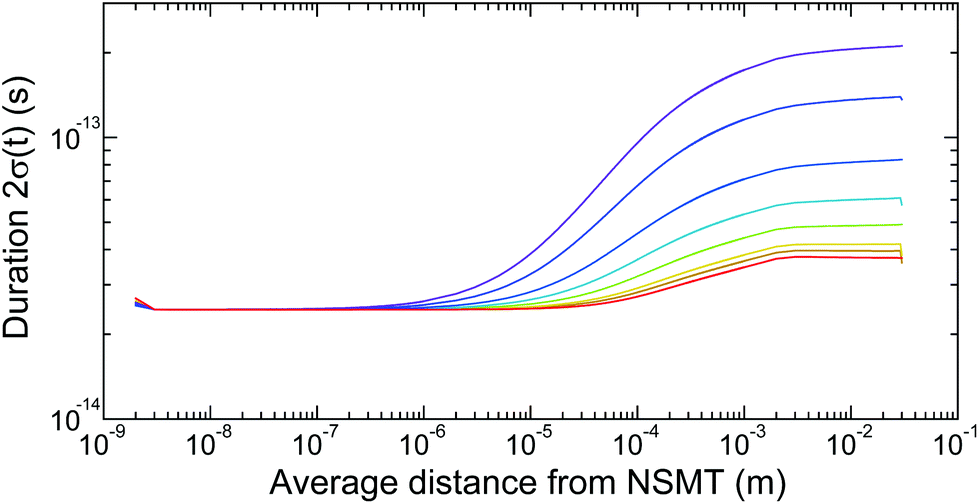 | ||
| Fig. 1 The 2σ(t) electron pulse duration as a function of average z position. The colour assignment from the lowest 2σ(t) is zero charge, then respectively 1e, 2e, 5e, 10e, 20e, 50e and 100 electrons per pulse. This colour coding is reused throughout. | ||
3.2 fs-TEM electron optics model
Defining performance goals for a high performance fs-TEM source is straightforward, being controllable divergence, short pulse duration, minimal space-charge distortion, high coherence and excellent beam quality. Defining similar criteria for the electron optics between the source and sample requires a series of often contradictory conditions to be met simultaneously, e.g. short duration requires a minimal flight length, which compromises the placement of magnetic lenses. Starting with a traditional TEM architecture and the design criteria in 1.2, we iteratively refined the geometry and element parameters (see section 2.1) until all conditions were met, resulting in the fs-TEM model presented in Fig. 2. The architecture presented has an inherent similarity to a TEM (acceleration region, transport lenses, condenser objective, sample and detector) albeit adapted for imaging in the time domain (pulsed laser driven source, temporal compressor).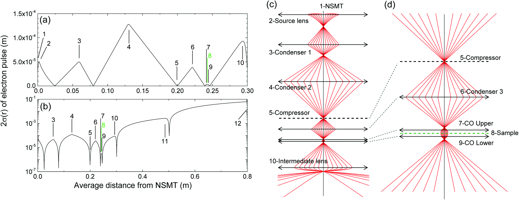 | ||
| Fig. 2 Configuration of the modelled fs-TEM instrument with elements identified: (1) NSMT electron source, (2) source lens, (3) condenser lens 1, C1, (4) condenser lens 2, C2, (5) temporal compressor, (6) condenser lens 3, C3, (7) upper part of condenser-objective magnetic lens, CO1, (8) sample plane, (9) lower part of condenser-objective, CO2, (10) intermediate lens, (11) projector lens and (12) electron detection plane. (a) 2σ(r) of the electron pulse as it propagates through the fs-TEM, where r is radial position in the x,y plane. (b) as (a) but over the full z-axis with 2σ(r) on a logarithmic scale. (c) Schematic of the electron pulse trajectory from the source to intermediate lens, where the back dashed line indicates the position of the temporal compressor at the focus of condenser 2. (d) as (c) but highlighting the condenser-objective and sample plane (green dashed line). | ||
For maximum instrument flexibility, parallel and convergent beams of varying diameter are required, hence we naturally turn to magnetic lenses which cause a focusing of a passing electron pulse via the Lorentz force. As discussed in section 3.3, changing the pulse charge dramatically influences duration, diameter and convergence or divergence. As the pulse charge is varied, the magnetic lens currents are optimised using the manual constraint and automated root finding from section 2.1. In Fig. 2, space charge is zero, however across the range of pulse parameters considered in sections 3.3 to 3.5, optimizations of the fs-TEM conditions place the spatial foci at the same locations, allowing comparison.
The desire to employ as much of the photoemitted flux from the NSMT for image creation rather than using apertures between the condenser lenses (section 3.1) means there is curvature of the electron pulse-front, a combination of the field around the NSMT and suppressor, along with the accelerating electric and focusing magnetic fields. The foci created after elements 2, 3 and 4 in Fig. 2 have a 2σ(r) of less than a micron in however exhibit a degree of spherical aberration, which is sufficient to prevent atomic resolution. It may be possible to remove this effect with multipole aberration correction, however that is beyond the scope of the current work. This effect is not a major issue other than around the sample, where we want the pulse-front to be as flat as possible, hence a simple condenser lens is insufficient. A condenser-objective (CO) lens, established in TEM for four decades, sees a converging beam passing through two (upper and lower) strong lenses acting to collimate the beam at the sample plane. We include such a lens, discussed in detail in section 3.5, which produces a collimated beam with radius 2σ(r) on the micron scale. Changing the C3 and CO lens currents facilitates variation of the sample spot size from 2σ(r) = 3 to 200 microns, with no other current adjustments.
Post-sample, intermediate and projector lenses provide magnification and deliver the pulse to the electron detector. As temporal information is encoded by a pump–probe measurement, the temporal resolution is a convolution of the pump laser and probe electron pulse durations at the sample, and the process under investigation. As long as no additional spatial distortion occurs, the process under investigation causes a deformation of the sample image as a function of pump–probe delay. The recovery of localized fields from such deformations has recently been described by Baum and co-workers. The accurate transport of this deformed image to the detector is aided by the temporal divergence of the electron pulse after the compressor, which reduces the charge density so the post-sample electron optics act akin to a TEM.
3.3 Propagating ultrafast electron pulses through magnetic lenses
As shown in Fig. 2, the electron pulses are sent through four spatial foci before interaction with the sample, inducing a high localised charge density. Passing through a spatial focus, the severity of temporal expansion depends on the incident pulse duration, number of electrons, beam size and convergence angle. We model the propagation of an electron pulse through a magnetic lens for a range of parameters, shown in Fig. 3. Rather than consider the full fs-TEM as shown in Fig. 2, we start a collimated electron pulse at z = 0 with an average energy of 70 keV and a bandwidth of 0.5 eV, and 2σ(r) = 50 μm. We are then able to see the influence of the single magnetic lens rather than having to consider alterations to the pulse during transport from the NSMT.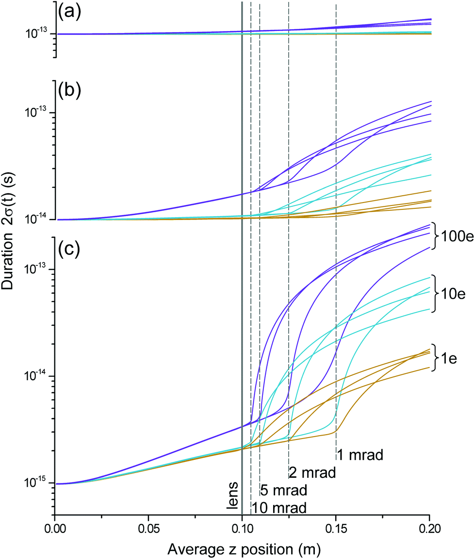 | ||
| Fig. 3 Temporal action of a range of magnetic lens strengths on a 70 keV electron pulse of varying initial duration and charge. The magnetic lens is at z = 0.1 m (solid line) and forms foci at z = 0.15 m (convergence angle of 1 mrad), z = 0.125 m (2 mrad), z = 0.11 m (5 mrad) and z = 0.105 m (10 mrad), indicated by dashed lines. (a) Initial duration of 2σ(t) = 100 fs. (b) Initial duration of 2σ(t) = 10 fs. (c) Initial duration of 2σ(t) = 1 fs. The 2σ(t) scale is comparable between panels, and the colour coding is as with Fig. 1. | ||
Pulses with 1, 10 and 100 electrons, for durations of 100, 10 and 1 fs, are shown in Fig. 3(a–c). A solenoid lens at z = 0.1 m focuses with convergence angles from 1 to 10 mrad. Some temporal stretching is observed between z = 0 and 0.1 m, and is most dramatic for the shortest pulse and highest charge. As apparent in Fig. 3(a), 100 fs electron pulses are distorted a moderate amount, with the most obvious influence on the highest charge. As seen in Fig. 3(b), a 10 fs, 1–100e pulse increases in duration by less than an order of magnitude over the range considered. Nonetheless, propagating a pulse of 100 electrons will be challenging if we want to retain a duration below ten femtoseconds.
For the 1 fs pulse shown in Fig. 3(c), the limited longitudinal dimension coupled with radial confinement due to the lens causes a rapid explosion in time. As the convergence angle is decreased from 10 mrad to 1 mrad, the duration increases more rapidly with increasing z. Furthermore, for low convergence foci and 10 and 100e pulses, the duration is distorted over a far larger z as compared to the high convergence foci.
Under design criteria 2 and 3, optimization of the number of electrons indicates around 10e per pulse is a good compromise, and an initial duration of the order 10 fs provides a good balance between minimal spatial focus-induced temporal distortion and compression requirement. Such a pulse repeatedly passing through foci would undergo most temporal distortion after the first focus, followed by successively reducing distortions as the duration increases. As seen in the following section, a pulse with a duration of high tens of femtoseconds is compressible to the extent that criteria 3 will still be met.
3.4 Temporal compression
Temporal control of the electron pulse duration is implemented passively via optimizations of the space-charge influence of each component and minimization of the total source to sample distance, and actively via a laser-driven THz resonator. Rather than numerically solve Maxwell's equations for a THz resonator, the influence of the compressor is modelled as a time-dependent momentum transfer to the pulse. A Gaussian momentum kick is applied along the electron propagation axis, rather than the 45 degree alignment of42,43 to minimize the streaking effect. A sinusoidal temporal variation is applied with a frequency of 0.3 THz, and the phase varied to optimize compression. In,42 optical field enhancement around the resonator yields electric fields of 106 V m−1, compressing picosecond electron pulses by a factor of 12 over a distance of tens of centimetres. Converting infrared laser radiation to THz pulses has a modest efficiency such that generating field strengths of 106 V m−1 in the resonator requires pulse energies of the order of 40 nJ at 0.3 THz, produced by focusing around 10 W at a wavelength of 1 μm within 1 ps at 50 kHz repetition rate.The action of the compressor is shown in Fig. 4 as the number of electrons per pulse and the peak electric field are varied. The electron pulse is generated at the NSMT as shown in Fig. 1 and the ESI,† and propagated to the compressor through condenser lenses 1 and 2, identified in Fig. 2. The changing electron density shifts the spatial foci of the source magnet, C1 and C2, so all pre-compressor optics are optimised for each pulse charge. The energy–time phase space representation is used to discuss the action of the compressor in the ESI.†
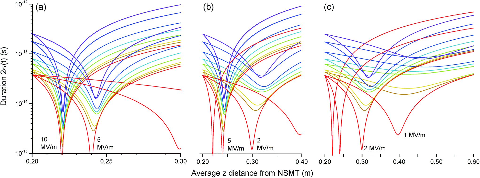 | ||
| Fig. 4 Active temporal compression mimicking the action of a terahertz resonator at z = 0.2 m with varying peak field strength and electron pulse charge. (a) Temporal foci for a peak field of 10 and 5 MV m−1 with an electron pulse charge varying from 0, 1e, 2e, 5e, 10e, 20e, 50e and 100e from lowest to highest 2σ(t). (b) as (a) for 5 and 2 MV m−1 and (c) as (a) for 2 and 1 MV m−1. | ||
At a peak electric field of 10 MV m−1 as shown in Fig. 4(a), pulses of up to 100e can be compressed to 2σ(t) < 10 fs. A peak field of 5 MV m−1 is less experimentally demanding, and as apparent from Fig. 4(a), electron pulses with a charge up to 20e can be compressed to a 2σ(t) < 10 fs. In Fig. 4(b), a peak field of 2 MV m−1 causes a further increase in compressed duration, whereby 1e and 2e pulses exhibit a duration of around 10 fs. This trend continues in Fig. 4(c), whereby 100e pulses approach a minimum of only 100 fs. As discussed earlier, the generation of such electron pulses at hundreds of kHz to few MHz repetition rates imposes a limit to the bunch charge.
The shifting z-position of the minimum duration with increasing pulse charge is a consequence of the spatio-temporal coupling of the charge density, whereby the spatial convergence of the pulse approaching the focus impacts the temporal distribution and vice versa, the peak electric field also defines the position of the temporal focus. We select a field strength of 5 MV m−1, which is an achievable compromise between compressor temporal performance and experimental feasibility. The expected factor of around ten is comparable to the recent work of Baum and co-workers,42 which has a lower bunch charge and longer initial pulse duration. At significantly higher compression fields, the electron pulse would compress to a shorter pulse, but over such a short distance so as to make subsequent focussing onto the sample plane extremely challenging.
We consider the practical realisation of the modelled instrument architecture in the ESI,† identifying the stability of the THz field as the most experimentally challenging aspect. The integration of the compressor into the fs-TEM column is also considered.
3.5 Condenser-objective lens implementation in fs-TEM
A condenser-objective (CO) lens combines the transport of the incoming electron pulse to the sample while also maximizing the post-sample divergence. A typical CO sees the sample placed equidistant between two strong magnetic windings, with B-fields approaching saturation in the soft metal circuits. These coils are excited by the same current, hence the symmetry of the lens collimates the beam at the sample, and are often coupled with an additional small condenser, manipulating the incoming convergence angle before the sample facilitating convergent or parallel illumination.To investigate the applicability of the CO lens to our model fs-TEM, we include a symmetric twin-field system with the sample equidistant between the condenser and the objective solenoids, shown in Fig. 2. Again, we do not include pole pieces in this design, rather take care so as maintain field strengths and gradients that can be managed with water-cooled lenses. We use the equivalent lens concept, whereby two solenoids of radius r separated by 2r is a good approximation of the field in a CO lens.
The influence of C3 and the CO is tested under two operating conditions, parallel and antiparallel current alignments. Referring to Fig. 2, C3 and the upper and lower parts of the CO have the same current direction in the former, and C3 and the CO lower are excited with opposite currents to the CO upper in the latter. The combined action of C3 and the CO upper collimates the pulse, which then passes a second focus after the sample as controlled by the CO lower, either by continuing to rotate about the z-axis or reversing direction.
A range of CO currents are specified between 1200 and 6600 Amp-turns, and then the C3 current is adjusted until the pulse is collimated at the sample plane, as detailed in the ESI.† All results are for a twenty electron pulse with an initial duration of 20 fs, space-charge is calculated without approximation, and all lenses and the compressor are optimised as the lens currents are adjusted. It is found that a focused electron pulse can also be formed at the sample plane, however we limit our discussion to parallel CO current alignment.
Systematically varying the C3 and CO currents changes the size of the collimated electron pulse at the sample plane. Parallel and anti-parallel current alignment pulse radii are shown in Fig. 5(a) and (b) respectively. Fig. 5(c) and (d) show the average angular velocity (proportional to the magnetic field) of the electron pulse in parallel and anti-parallel alignments. Parallel alignment is straightforward to achieve as the gradients required are less than in the anti-parallel case. Nonetheless, anti-parallel alignment has the significant advantage of forming a magnetic field zero at the sample plane, advantageous when observing laser-induced magnetism. The gradient between the minimum and maximum angular velocities in Fig. 5(d) is approximately linear, causing the reduction of 2σ(r) around the sample found in Fig. 5(b).
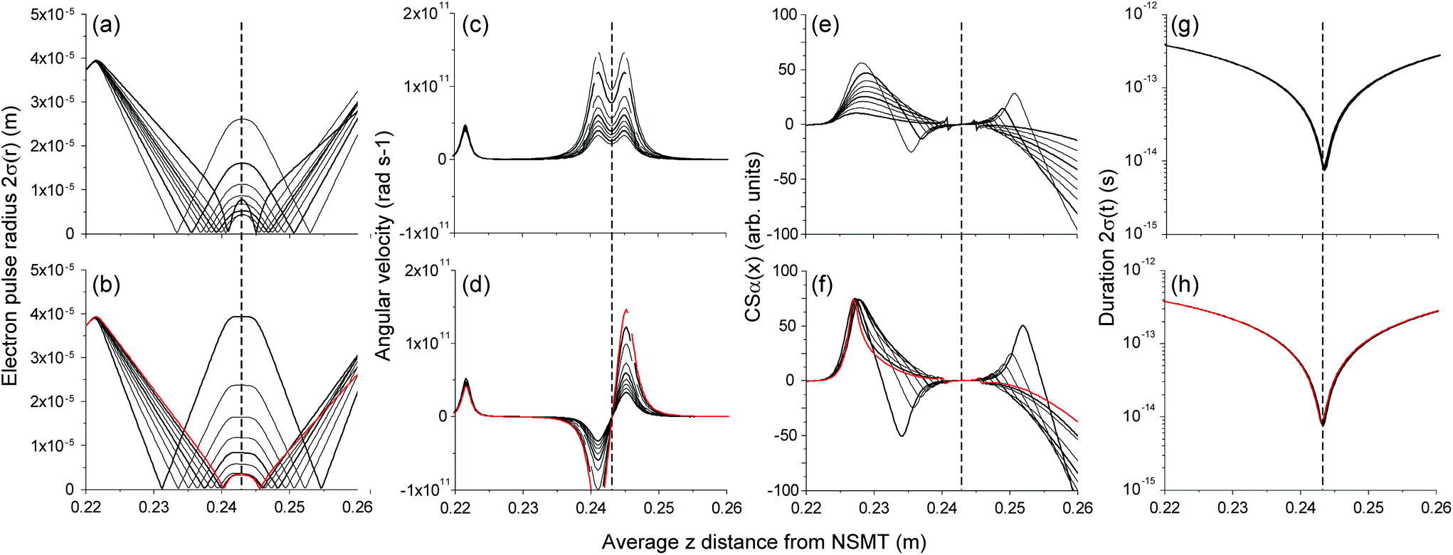 | ||
| Fig. 5 Spatial and temporal performance of the fs-TEM in the vicinity of the sample (indicated by vertical dashed line), with the top panels are parallel current alignment, and the bottom panels are for anti-parallel alignment. (a, b) 2σ(r) beam radius, (c, d) average angular velocity of the electron pulse, (e, f) Cournat–Snyder alpha parameter and (g, h) 2σ(t) temporal duration. The bold lines are referenced to the filled points in ESI Fig. A2,† and the red line indicates the lowest 2σ(r) achieved. | ||
The collimation characteristics in parallel and anti-parallel current alignments are shown in Fig. 5(e) and (f). The Courant–Snyder α-parameter (CSα) describes the correlation of the root mean squared particle position and direction. When CSα = 0, the electron pulse is either collimated or at a spatial focus. In Fig. 5(e) and (f), CSα crosses zero at the sample plane.
The action of the compressor is shown in Fig. 5(g) and (h), whereby the THz field strength and phase are set to achieve a temporal focus in the sample plane. The combined action of the CO and compressor is therefore a collimated electron pulse with 2σ(r) = 3 μm, and in the case of these 20e pulses, a 2σ(t) duration of 8.2 fs. Importantly, the influence of the CO and compressor are essentially independent, as apparent from Fig. 5(g) and (h). Comparing Fig. 3 and 5(h), the electron pulse propagating through the focus between C3 and the CO experiences a convergence angle between 2 and 4 mrad, and over the z-axis range of 0.01 m, the duration varies between 200 fs and 40 fs. As shown in Fig. 3, if 2σ(t) = 100 fs, there is very little temporal influence on the pulse duration at spatial focus. For 2σ(t) = 10 fs, the duration is perturbed by only a few femtoseconds.
3.6 Spatial resolution and dynamic electric field effects
The spatial resolution of the modelled fs-TEM will be loosely defined by the assumed pixel size and number, and size of detector, as discussed in section 2.1. Typical performance and magnification of a state of the art directly coupled camera implies achieving a resolution of 1 nm is likely to be practical.More informatively, we estimate the influence of spherical aberration on the spatial resolution: summing the electron pulse Airy disk and spherical aberration in quadrature gives an indication of spatial resolution, estimated from TEM lens performance.55 For an electron wavelength of 4.5 pm and a typical spherical aberration coefficient CS = 3 mm, an optimal convergence angle of 4.5 mrad is found, corresponding to an optimal resolution of 0.7 nm. We do not apply apertures along the electron path, resulting in an inherent curvature, which increases the effective CS to of the order of 10 mm, corresponding to an optimal resolution of approximately 1.2 nm.
Considering chromatic influences on resolution, taking the chromatic aberration coefficient CC to be, to a first order approximation, comparable to CS, the chromatic aberration is of the order 0.14 nm. However, the action of the THz compressor causes an energy–time phase space redistribution, increasing the energy bandwidth by the compression factor, hence the spatial resolution will, in a practical instrument design, dominate the spatial resolution.
It is suggested that the spatial resolution of a fs-TEM will be improved with multipole aberration correction such as used in state-of-the-art TEM systems to achieve atomic resolution, but used to mitigate the conservation of energy–time phase space. Such a corrector will introduce tens of cm additional flight length, however as shown in Fig. 3 and discussed earlier, once an electron pulse of tens to hundreds of femtoseconds in duration has passed through one focus, subsequent stretching is mitigated. As a result, the introduction of a multi-pole corrector is expected to have only a moderate impact on the instrument performance, and is the subject of a current investigation.
When propagating macroparticles representing the electron pulse, GPT assigns a particle identification number, Np, which varies between 1 and 250 for these calculations. In Fig. 6, the variation of Np as a function of radial distance and macroparticle arrival times at both the sample and detector planes is shown. This then highlights the importance of the performance of a CO lens in a fs-TEM system as the wavefront is flat, thus the imprint of the sample can be successfully transferred to the electron pulse.
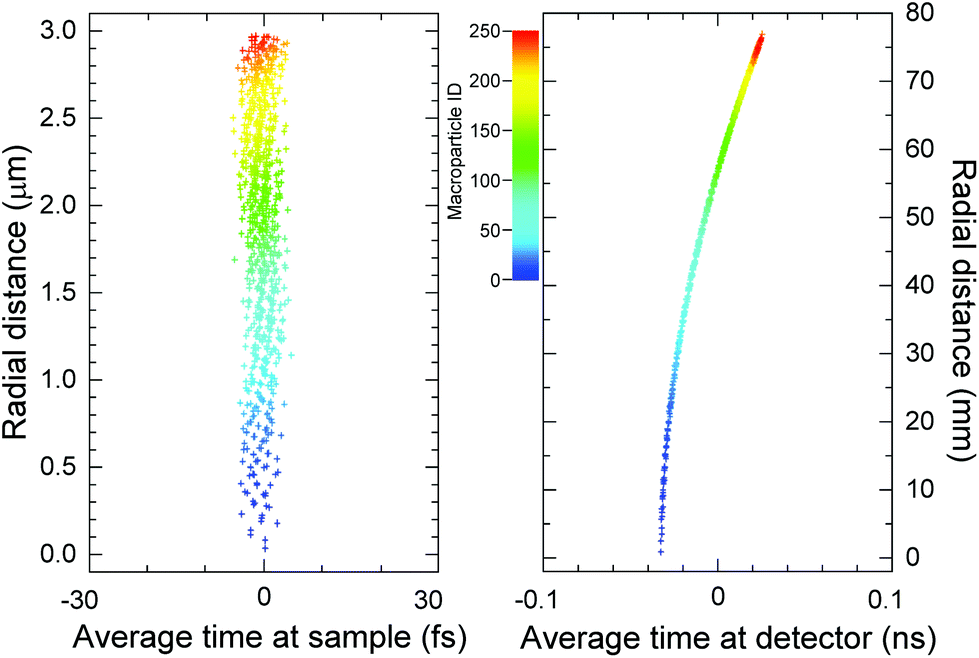 | ||
| Fig. 6 Electron pulse spatial distribution at (a) sample and (b) detector. The colour scale is macroparticle identification number, indicating the transfer of information from the sample to detector plane. | ||
As the electron pulse passes the sample plane, it will be scattered and attenuated by the morphology of the nanoscale structure, which is considered to be constant as a function of time. Applying the pump laser pulse to the nanoscale structure will induce localized transient electric and magnetic fields, which might be a result of, for example, liberation of charge through tunnelling, ultrafast plasmonic effects, and the formation of short lived magnetic domains. The temporal overlap of these localized fields with the passing electron pulse introduces a dynamic scattering, which will vary with laser-pump and electron-probe delay, and will allow the quantification of the transient field strength and direction.
To exploit the imaging capabilities of the modelled fs-TEM, the detection of electromagnetic fields requires quantification. A custom GPT element deflects the passing electron pulse with an electric field, and removes macroparticles from the pulse if they pass the sample plane within an annular boundary, mimicking a prototype structure as shown in Fig. 7(a). The direction and strength of the electric field in the xy plane (mutually perpendicular to the z-axis) is indicated by the arrows. The shaded region is the annulus, opaque to electrons, hence is thick as compared to the mean free path of the electrons at 70 keV.
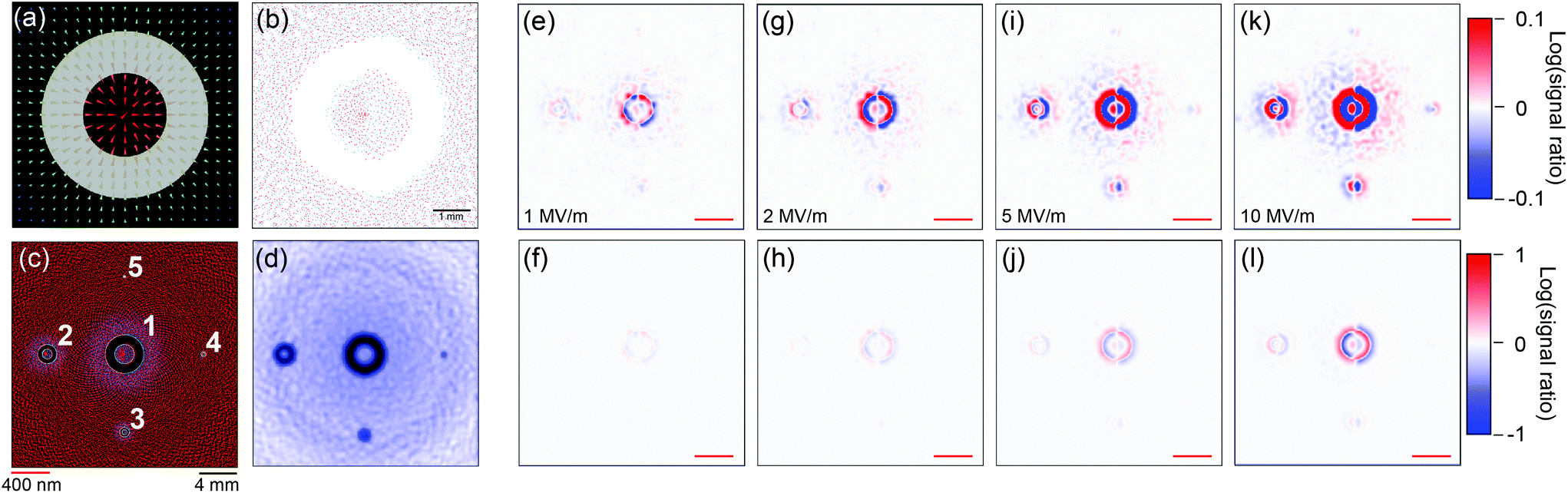 | ||
Fig. 7 fs-TEM imaging of electric fields at the sample plane. (a) Schematic of the scattering element, with the vector field Escat strength represented by arrow colour and size. (b) Typical macroparticle scattering maps at the detector plane. The green points are the unscattered macroparticles (i.e. Escat = 0) and red are scattered by the element in (a) with Escat = 10 MV m−1. (c) Location of five scattering elements of varying size: (i = 1) outer![[thin space (1/6-em)]](https://www.rsc.org/images/entities/char_2009.gif) :inner radii of 200:100 nm, (i = 2) 100:50 nm, (i = 3) 50:25 nm, (i = 4) 20:10 nm and (i = 5) 10:5 nm outer and inner radii respectively. (d) Gaussian convolution applied to a macroparticle distribution with a standard deviation σ = 350 μm at the sample plane, recreating an undersampled fs-TEM image. (e, f) Logarithm of the ratio of the unscattered to scattered fs-TEM images with Escat = 1 MV m−1. (g, h) as (e, f) but for Escat = 2 MV m−1. (i, j) Escat = 5 MV m−1, and (k, l) Escat = 10 MV m−1. Red areas indicate an increase in signal whereas blue areas indicate a deficit, and the red scale bar is 400 nm. :inner radii of 200:100 nm, (i = 2) 100:50 nm, (i = 3) 50:25 nm, (i = 4) 20:10 nm and (i = 5) 10:5 nm outer and inner radii respectively. (d) Gaussian convolution applied to a macroparticle distribution with a standard deviation σ = 350 μm at the sample plane, recreating an undersampled fs-TEM image. (e, f) Logarithm of the ratio of the unscattered to scattered fs-TEM images with Escat = 1 MV m−1. (g, h) as (e, f) but for Escat = 2 MV m−1. (i, j) Escat = 5 MV m−1, and (k, l) Escat = 10 MV m−1. Red areas indicate an increase in signal whereas blue areas indicate a deficit, and the red scale bar is 400 nm. | ||
The scattering electric field decreases radially in the xy plane from a central maximum of Escat following a Gaussian distribution, σr which scales with annulus outer radius. The field direction rotates linearly with θ until a direction reversal at θ = 0 and π radians, with θ being angle in the xy plane. The scattering field is Gaussian along the z-axis with a standard deviation σz = 100 nm, a thickness chosen to represent the distance over which a nanoscale photonically active structure would exhibit a dynamic field. There is no time dependence to Escat, however the convolution of the temporal duration of the electron pulse of 2σ(t) = 8.2 fs with the 100 nm thickness at 70 keV implies an interaction time with a 2σ(t) = 9.3 fs.
The influence of both the opaque region and localized electric field is shown in Fig. 7(b), where the point of arrival of the macroparticles at the detector are indicated by a point. The green points are the field-free case, and the red points indicate the modified trajectories caused by a scattering field Escat = 10 MV m−1. The geometry of the annuluses from i = 1 to i = 5 in the format outer radius (nm):inner radius (nm) shown in Fig. 7(c) are (i = 1) 200:100, (i = 2) 100:50, (i = 3) 50:25, (i = 4) 20:10 and (i = 5) 10:5. We compare pulses that have been deflected (Escat ≠ 0) with those which have not (Escat = 0) yielding the discrete displacements maps shown in Fig. 7(b).
To convert the discrete macroparticle representation to a continuous image, a convolution with a Gaussian kernel of standard deviation, σ = 350 μm is applied, and is the conversion from Fig. 7(c)–(d). This is a blurred and undersampled image because the Gaussian convolution is constrained by the number of macroparticles used in the numerical propagation, which in the case of Fig. 7 is N = 20000. The standard deviation of the convolution is an overestimate as compared to what can be achieved with an optimised direct detector, which as discussed in 1.1, is below 10 μm. This artificial spatial blur is necessary as N = 20000 is at least approximately 50 times lower than would be wanted for image formation, a limitation applied as the execution time of calculations scales as N2. The structures present in the detection event distributions in Fig. 7(c) and (d) are artefacts from the Hammersley sequence used.56
To create the signal maps shown in Fig. 7(e)–(l), the Escat ≠ 0 maps are divided by the Escat = 0 map, and the logarithm taken. Field strengths Escat = 1, 2, 5 and 10 MV m−1 (e & f, g & h, i & j and k & l respectively) are displayed on two ranges, here an order of magnitude and a tenth of an order. It is apparent from Fig. 7 that dynamic electric fields of 1 MV m−1 will be resolvable. Clearly this depends on the signal to noise ratio of the observation; however in principle such thin and fast acting fields appear observable. Given the undersampling condition discussed above and the spatial resolution of around 1 nm, it is expected that weaker fields over smaller distances will be resolvable. An electric field of 10 MV m−1 corresponds to a surface charge density of around 10e per μm2, which overlaps well with the strength of field generated in many electronic devices, along with those achievable in ultrafast nanophotonics.
Fig. 8 summarises the performance of the fs-TEM for two illumination modes, corresponding to the largest and smallest 2σ(r) in Fig. 5(b), as the number of electrons per pulse is varied. For durations of approximately 10 fs for low tens of electrons per pulse, a small variation in 2σ(r) ≈ 3.2 μm and ≈39 μm, indicating that variations in the charge per pulse will have a minimal influence on spatial resolution if of the order of 20%. The pulse durations for both radii are displayed upon entrance to the resonator and at the sample plane, indicating the level of compression achieved. We find that pulse compression by a factor greater than 10 is achievable, yielding a 2σ(t) ≈ 10 fs, for pulses containing up to 20 electrons. The independence of temporal and spatial resolutions are seen from the overlap between the larger electron beam (white triangles) and smaller (solid black squares) in Fig. 8(c). Variation of the charge per pulse will influence the compressed duration as apparent from Fig. 8(c), which has a gradient of approximately 1:2.5, hence, a finite width distribution of charge per pulse results in a distribution of durations increased by 1:2.5. Practical instrument design must take such considerations into account, as discussed in more detail in the ESI.†
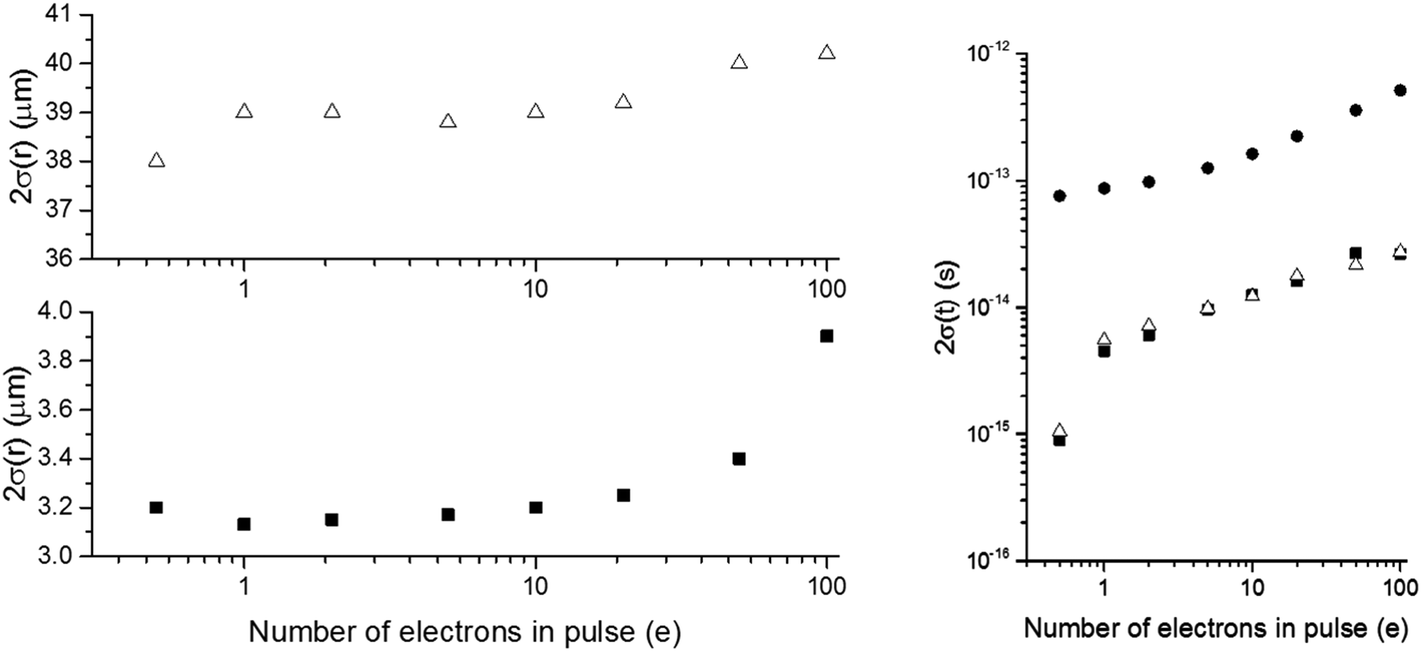 | ||
| Fig. 8 fs-TEM performance as a function of pulse charge under two collimated imaging conditions with anti-parallel C3 and CO excitation. (a) Large beam CO setting. (b) Small beam CO setting. (c) Duration at sample plane for both large (open triangle) and small (filled square) beams, compared to the pulse duration approaching the resonator (filled circle). | ||
4. Conclusions
In conclusion, we have reported the outcome of a numerical study of a femtosecond transmission electron microscope. We find that for a pulse containing twenty electrons, a sub-10 fs duration can be achieved, and that a spatial resolution of the order of one nanometre is feasible. Simulations from the femtosecond electron pulse source to the detector were presented, and the optimization of each beamline component has resulted in an apparatus architecture for a compact, high performance, table-top scale instrument. Optical compression of the electron pulse at a terahertz resonator have been included in the model, showing how the dispersive influence of space charge can be overcome. Relying on the all-optical triggering of the photoemission, compression and sample pumping means that a temporal jitter of the order of a femtosecond is achievable.Femtosecond-TEM performance has been investigated for a variety of pulse characteristics, allowing the tailoring to the application whilst maximising the photoelectron current delivered to the sample, ensuring viable imaging times. The system is envisioned to run at tens of kilohertz to megahertz repetition rates due to the relatively low charge densities utilised, but within the achievable limits of brightness possible with laser driven emission from NSMTs. We model the outcome of using the fs-TEM pulses to image a transient electric field at the sample plane, finding that 1 MV m−1 is readily resolvable, and with improvements to the simulation conditions, smaller fields should be resolvable on a nanometre scale.
The spatial, temporal and field resolution of the fs-TEM are appropriate to visualise ultrafast processes in the coupled fields of nanophotonics and optical computing, resolve coherent optical and acoustic phonon dynamics in organic and inorganic samples, laser-induced magnetism dynamics in nanostructures and thin films, and potentially the tracking of charge carrier dynamics in photovoltaics and organic optoelectronic devices. As a consequence, will see broad applicability to a wide variety of light-triggered applications, and should open new scientific avenues of investigation.
Conflicts of interest
There are no conflicts to declare.Acknowledgements
CWBM acknowledges a College of Science Postgraduate Research Scholarship, NJP acknowledges an Undergraduate Summer Placement Scholarship, and WAB wishes to thank the Engineering and Physical Sciences Research Council (EPSRC, UK) for funding through EP/K031619/1, and support through EP/G03088X/1.References
- M. Th. Hassan, Attomicroscopy: from femtosecond to attosecond electron microscopy, J. Phys. B: At., Mol. Opt. Phys., 2018, 51, 032005, DOI:10.1088/1351-6455/aaa183.
- G. Sciaini and R. J. D. Miller, Femtosecond electron diffraction: heralding the era of atomically resolved dynamics, Rep. Prog. Phys., 2011, 74, 096101 CrossRef.
- A. H. Zewail, 4D ultrafast electron diffraction, crystallography, and microscopy, Annu. Rev. Phys. Chem., 2006, 57, 65–103, DOI:10.1146/annurev.physchem.57.032905.104748.
- W. E. King, G. H. Campbell, A. Frank, B. Reed, J. F. Schmerge, B. J. Siwick, B. C. Stuart and P. M. Weber, Ultrafast electron microscopy in materials science, biology, and chemistry, J. Appl. Phys., 2005, 97, 111101 CrossRef.
- V. A. Lobastov, R. Srinivasan and A. Zewail, Four-dimensional ultrafast electron microscopy, Proc. Natl. Acad. Sci. U. S. A., 2005, 102, 7069–7073 CrossRef CAS PubMed.
- E. Quinonez, J. Handali and B. Barwick, Femtosecond photoelectron point projection microscope, Rev. Sci. Instrum., 2013, 84, 103710, DOI:10.1063/1.4827035.
- M. Müller, A. Paarmann and R. Ernstorfer, Femtosecond electrons probing currents and atomic structure in nanomaterials, Nat. Commun., 2014, 5, 5292, DOI:10.1038/ncomms6292.
- M. Müller, V. Kravtsov, A. Paarmann, M. B. Raschke and R. Ernstorfer, Nanofocused plasmon-driven sub-10 fs electron point source, ACS Photonics, 2016, 3, 611–619, DOI:10.1021/acsphotonics.5b00710.
- J. Vogelsang, J. Robin, B. J. Nagy, P. Dombi, D. Rosenkranz, M. Schiek, P. Groß and C. Lienau, Ultrafast electron emission from a sharp metal nanotaper driven by adiabatic nanofocusing of surface plasmons, Nano Lett., 2015, 15, 4685–4691, DOI:10.1021/acs.nanolett.5b01513.
- A. R. Bainbridge, C. W. Barlow Myers and W. A. Bryan, Femtosecond few- to single-electron point-projection microscopy for nanoscale dynamic imaging, Struct. Dyn., 2016, 3, 023612, DOI:10.1063/1.4947098.
- P. Hommelhoff, Y. Sortais, A. Aghajani-Talesh and M. A. Kasevich, Field emission tip as a nanometer source of free electron femtosecond pulses, Phys. Rev. Lett., 2006, 96, 077401 CrossRef PubMed.
- P. Hommelhoff, C. Kealhofer and M. A. Kasevich, Ultrafast electron pulses from a tungsten tip triggered by low-power femtosecond laser pulses, Phys. Rev. Lett., 2006, 97, 247402 CrossRef PubMed.
- C. Ropers, D. R. Solli, C. P. Schulz, C. Lienau and T. Elsaesser, Localized multiphoton emission of femtosecond electron pulses from metal nanotips, Phys. Rev. Lett., 2007, 98, 043907 CrossRef CAS PubMed.
- M. Schenk, M. Krüger and P. Hommelhoff, Strong-field above-threshold photoemis- sion from sharp metal tips, Phys. Rev. Lett., 2010, 105, 257601 CrossRef PubMed.
- H. Yanagisawa, C. Hafner, P. Dona, M. Klockner, D. Leuenberger, T. Greber, J. Osterwalder and M. Hengsberger, Laser-induced field emission from a tungsten tip: Optical control of emission sites and the emission process, Phys. Rev. B: Condens. Matter Mater. Phys., 2010, 81, 115429, DOI:10.1103/PhysRevB.81.115429.
- H. Yanagisawa, M. Hengsberger, D. Leuenberger, M. Klockner, C. Hafner, T. Greber and J Osterwalder, Energy distribution curves of ultrafast laser-induced field emission and their im- plications for electron dynamics, Phys. Rev. Lett., 2011, 107, 087601, DOI:10.1103/PhysRevLett.107.087601.
- R. Bormann, M. Gulde, A. Weismann, S. V. Yalunin and C. Ropers, Tip-enhanced strong-field photoemission, Phys. Rev. Lett., 2010, 105, 147601 CrossRef CAS PubMed.
- M. Krüger, M. Schenk and P. Hommelhoff, Attosecond control of electrons emitted from a nanoscale metal tip, Nature, 2011, 475, 78–81 CrossRef PubMed.
- D. Ehberger, J. Hammer, M. Eisele, M. Krüger, J. Noe, A. Högele and P. Hommelhoff, Highly coherent electron beam from a laser-triggered tungsten needle tip, Phys. Rev. Lett., 2015, 114, 227601 CrossRef PubMed.
- A. Paarmann, M. Gulde, M. Muller, S. Schäfer, S. Schweda, M. Maiti, C. Xu, T. Hohage, F. Schenk, C. Ropers and R. Ernstorfer, Coherent femtosecond low-energy single-electron pulses for time-resolved diffraction and imaging: a numerical study, J. Appl. Phys., 2012, 112, 113109–113110 CrossRef.
- R. Bormann, S. Strauch, S. Schafer and C. Ropers, An ultrafast electron microscope gun driven by two-photon photoemission from a nanotip cathode, J. Appl. Phys., 2015, 118, 173105 CrossRef.
- S. A. Hilbert, A. Neukirch, C. J. G. J. Uiterwaal and H. Batelaan, Exploring temporal and rate limits of laser-induced electron emission, J. Phys. B: At., Mol. Opt. Phys., 2009, 42, 141001 CrossRef.
- S. P. Weathersby, G. Brown, M. Centurion, T. F. Chase, R. Coffee, J. Corbett, J. P. Eichner, J. C. Frisch, A. R. Fry, M. Gühr, N. Hartmann, C. Hast, R. Hettel, R. K. Jobe, E. N. Jongewaard, J. R. Lewandowski, R. K. Li, A. M. Lindenberg, I. Makasyuk, J. E. May, D. McCormick, M. N. Nguyen, A. H. Reid, X. Shen, K. Sokolowski-Tinten, T. Vecchione, S. L. Vetter, J. Wu, J. Yang, H. A. Dürr and X. J. Wang, Mega-electron-volt ultrafast electron diffraction at SLAC National Accelerator Laboratory, Rev. Sci. Instrum., 2015, 86, 73702, DOI:10.1063/1.4926994.
- P. Musumeci, J. T. Moody, C. M. Scoby, M. S. Gutierrez, H. A. Bender and N. S. Wilcox, High quality single shot diffraction patterns using ultrashort megaelectron volt electron beams from a radio frequency photoinjector, Rev. Sci. Instrum., 2010, 81, 13306, DOI:10.1063/1.3292683.
- P. Zhu, Y. Zhu, Y. Hidaka, L. Wu, J. Cao, H. Berger, J. Geck, R. Kraus, S. Pjerov, Y. Shen, R. I. Tobey, J. P. Hill and X. J. Wang, Femtosecond time-resolved MeV electron diffraction, New J. Phys., 2015, 17, 063004, DOI:10.1088/1367-2630/17/6/063004.
- H. Dömer and O. Bostanjoglo, High-speed transmission electron microscope, Rev. Sci. Instrum., 2003, 74, 4369, DOI:10.1063/1.1611612.
- A. H. Zewail, Four-dimensional electron microscopy, Science, 2010, 328, 187–193, DOI:10.1126/science.1166135.
- N. D. Browning, M. A. Bonds, G. H. Campbell, J. E. Evans, T. LaGrange, K. L. Jungjohann, D. J. Masiel, J. McKeown, S. Mehraeen, B. W. Reed and M. Santala, Recent developments in dynamic transmission electron microscopy, Curr. Opin. Solid State Mater. Sci., 2012, 16, 23–30, DOI:10.1016/j.cossms.2011.07.001.
- B. Barwick, H. S. Park, O. Kwon, J. S. Baskin and A. H. Zewail, 4D imaging of transient structures and morphologies in ultrafast electron microscopy, Science, 2008, 322, 1227–1231, DOI:10.1126/science.1164000.
- J. S. Kim, T. LaGrange, B. W. Reed, M. L. Taheri, M. R. Armstrong, W. E. King, N. D. Browning and G. H. Campbell, Imaging of transient structures using nanosecond in situ TEM, Science, 2008, 321, 1472–1475, DOI:10.1126/science.1161517.
- M. R. Armstrong, K. Boyden, N. D. Browning, G. H. Campbell, J. D. Colvin, W. J. DeHope, A. M. Frank, D. J. Gibson, F. Hartemann, J. S. Kim, W. E. King, T. B. LaGrange, B. J. Pyke, B. W. Reed, R. M. Shuttlesworth, B. C. Stuart and B. R. Torralv, Practical considerations for high spatial and temporal resolution dynamic transmission electron microscopy, Ultramicroscopy, 2007, 107, 356–367 CrossRef CAS PubMed.
- A. Feist, K. E. Echternkamp, J. Schauss, S. V. Yalunin, S. Schäfer and C. Ropers, Quantum coherent optical phase modulation in an ultrafast transmission electron microscope, Nature, 2015, 521, 200–203, DOI:10.1038/nature14463.
- L. Piazza, D. J. Masiel, T. LaGrange, B. W. Reed, B. Barwick and F. Carbone, Design and implementation of a fs-resolved transmission electron microscope based on thermionic gun technology, Chem. Phys., 2013, 423, 79–84, DOI:10.1016/j.chemphys.2013.06.026.
- E. Kieft, K. B. Schliep, P. K. Suri and D. J. Flannigan, Communication: effects of thermionic-gun parameters on operating modes in ultrafast electron microscopy, Struct. Dyn., 2015, 2, 51101, DOI:10.1063/1.4930174.
- G. Cao, S. Sun, Z. Li, H. Tian, H. Yang and J. Li, Clocking the anisotropic lattice dynamics of multi-walled carbon nanotubes by four-dimensional ultrafast transmission electron microscopy, Sci. Rep., 2015, 5, 8404, DOI:10.1038/srep08404.
- K. Bücker, M. Picher, O. Crégut, T. LaGrange, B. W. Reed, S. T. Park, D. J. Masiel and F. Banhart, Electron beam dynamics in an ultrafast transmission electron microscope with Wehnelt electrode, Ultramicroscopy, 2016, 17, 8–18, DOI:10.1016/j.ultramic.2016.08.014.
- M. Kuwahara, Y. Nambo, K. Aoki, K. Sameshima, X. Jin, T. Ujihara, H. Asano, K. Saitoh, Y. Takeda and N. Tanaka, The Boersch effect in a picosecond pulsed electron beam emitted from a semiconductor photocathode, Appl. Phys. Lett., 2016, 109, 13108, DOI:10.1063/1.4955457.
- F. Houdellier, G. M. Caruso, P. Abeilhou and A. Arbouet, Design and realization of an ultrafast cold field emission source operating under high voltage, Proceedings of the 16th Eur. Microsc. Congr., Lyon, France, 2016. DOI:10.1002/9783527808465.EMC2016.4759.
- A. Feist, N. Bach, N. R. d. Silva, T. Danz, M. Möller, K. E. Priebe, T. Domröse, J. Gre-gor, S. R. Gatzmann, J. Schauss, S. Strauch, R. Bormann, M. Sivis, S. Schäfer and C. Ropers, Ultrafast transmission electron microscopy using a laser-driven field emitter: femtosecond resolution with a high coherence electron beam, Ultramicroscopy, 2017, 176, 63–73 CrossRef CAS PubMed.
- G. M. Caruso, F. Houdellier, P. Abeilhou and A. Arbouet, Development of an ultrafast electron source based on a cold-field emission gun for ultrafast coherent TEM, Appl. Phys. Lett., 2017, 111, 023101 CrossRef.
- F. Houdellier, G. M. Caruso, S. Weber, M. Kociak and A. Arbouet, Development of a high brightness ultrafast Transmission Electron Microscope based on a laser-driven cold field emission source, Ultramicroscopy, 2018, 186, 128–138, DOI:10.1016/j.ultramic.2017.12.015.
- C. Kealhofer, W. Schneider, D. Ehberger, A. Ryabov, F. Krausz and P. Baum, All-optical control and metrology of electron pulses, Science, 2016, 352, 429–433, DOI:10.1126/science.aae0003.
- A. Ryabov and P. Baum, Electron microscopy of electromagnetic waveforms, Science, 2016, 353, 374–377, DOI:10.1126/science.aaf8589.
- D. Zhang, A. Fallahi, M. Hemmer, X. Wu, M. Fakhari, Y. Hua, H. Cankaya, A. Calendron, L. E. Zapata, N. H. Matlis and F. X. Kärtner, Segmented terahertz electron accelerator and manipulator (STEAM), Nat. Photonics, 2018, 12, 336–342 CrossRef CAS PubMed.
- K. E. Priebe, C. Rathje, S. V. Yalunin, T. Hohage, A. Feist, S. Schafer and C. Ropers, Attosecond electron pulse trains and quantum state reconstruction in ultrafast transmission electron microscopy, Nat. Photonics, 2017, 11, 793–797 CrossRef CAS.
- Y. Morimoto and P. Baum, Diffraction and microscopy with attosecond electron pulse trains, Nat. Phys., 2018, 14, 252–256 Search PubMed.
- Y. Morimoto and P. Baum, , Attosecond control of electron beams at dielectric and absorbing membranes, Phys. Rev. A, 2018, 97, 033815, DOI:10.1103/PhysRevA.97.033815.
- T. van Oudheusden, P. L. E. M. Pasmans, S. B. van der Geer, M. J. de Loos, M. J. van der Wiel and O. J. Luiten, Compression of Subrelativistic Space-Charge-Dominated Electron Bunches for Single-Shot Femtosecond Electron Diffraction, Phys. Rev. Lett., 2010, 105, 264801, DOI:10.1103/PhysRevLett.105.264801.
- O. J. Luiten, S. B. van der Geer, M. J. de Loos, F. B. Kiewiet and M. J. van der Wiel, How to Realize Uniform Three-Dimensional Ellipsoidal Electron Bunches, Phys. Rev. Lett., 2004, 93, 094802, DOI:10.1103/PhysRevLett.93.094802.
- K. Halbach and R. F. Holsinger, Superfish – a computer program for evaluation of RF cavities with cyindircal symmetry, Part. Accel., 1976, 6, 213–222 Search PubMed . http://laacg.lanl.gov/laacg/services/download_sf.phtml.
- M. J. de Loos and S. B. van der Geer, General Particle Tracer : a new 3D code for accelerator and beamline design, in Proceedings of EPAC 1996, Sitges, Spain, 1996, p. 1241, http://www.pulsar.nl/gpt Search PubMed.
- A. R. Bainbridge and W. A. Bryan, Velocity map imaging of femtosecond laser induced photoelectron emission from metal nanotips, New J. Phys., 2014, 16, 103031, DOI:10.1088/1367-2630/16/10/103031.
- J. Hoffrogge, J. Paul Stein, M. Kruger, M. Forster, J. Hammer, D. Ehberger, P. Baum and P. Hommelhoff, Tip-based source of femtosecond electron pulses at 30 keV, J. Appl. Phys., 2014, 115, 094506 CrossRef.
- B. Schroder, M. Sivis, R. Bormann, S. Schafer and C. Ropers, An ultrafast nanotip electron gun triggered by grating-coupled surface plasmons, Appl. Phys. Lett., 2015, 107, 231105 CrossRef.
- D. B. Williams and C. B. Carter, Transmission Electron Microscopy, Springer, 2009 Search PubMed.
- J. M. Hammersley, Monte-Carlo methods for solving multivariable problems, Ann. N. Y. Acad. Sci., 1960, 86, 844–874 CrossRef.
Footnote |
| † Electronic supplementary information (ESI) available. See DOI: 10.1039/c8nr06235h |
| This journal is © The Royal Society of Chemistry 2018 |