
 Open Access Article
 This Open Access Article is licensed under a Creative Commons Attribution-Non Commercial 3.0 Unported Licence
Defect-free SnTe topological crystalline insulator nanowires grown by molecular beam epitaxy on graphene
Janusz
Sadowski
 *abc,
Piotr
Dziawa
a,
Anna
Kaleta
a,
Bogusława
Kurowska
a,
Anna
Reszka
a,
Tomasz
Story
a and
Sławomir
Kret
*a
*abc,
Piotr
Dziawa
a,
Anna
Kaleta
a,
Bogusława
Kurowska
a,
Anna
Reszka
a,
Tomasz
Story
a and
Sławomir
Kret
*a
aInstitute of Physics, Polish Academy of Sciences, Aleja Lotnikow 32/46, PL-02668 Warszawa, Poland. E-mail: janusz.sadowski@ifpan.edu.pl; kret@ifpan.edu.pl
bDepartment of Physics and Electrical Engineering, Linnaeus University, SE-391 82 Kalmar, Sweden
cMAX-IV Laboratory, Lund University, P.O. Box 118, SE-221 00 Lund, Sweden
First published on 11th October 2018
Abstract
SnTe topological crystalline insulator nanowires have been grown by molecular beam epitaxy on graphene/SiC substrates. The nanowires have a cubic rock-salt structure, they grow along the [001] crystallographic direction and have four sidewalls consisting of {100} crystal planes known to host metallic surface states with a Dirac dispersion. Thorough high resolution transmission electron microscopy investigations show that the nanowires grow on graphene in the van der Waals epitaxy mode induced when the catalyzing Au nanoparticles mix with Sn delivered from a SnTe flux, providing a liquid Au–Sn alloy. The nanowires are totally free from structural defects, but their {001} sidewalls are prone to oxidation, which points out the necessity of depositing a protective capping layer in view of exploiting the magneto-electric transport phenomena involving charge carriers occupying topologically protected states.
1. Introduction
SnTe belongs to a very well-known family of narrow bandgap IV–VI semiconductors, which have been studied because of their interesting electronic properties1 and applications, e.g. in thermoelectric energy harvesting and as mid-infrared detectors and emitters.2 Quite recently SnTe and some of its ternary (multinary) alloys with Se and/or Pb were identified as topological crystalline insulators (TCI).3 Indeed IV–VI TCIs host topologically protected Dirac surface states in the vicinity of the distinct points of the Brillouin zone (in this case projection of the L points on the surface Brillouin zone). These states occur due to the coexistence of specific crystalline symmetries, i.e. {110} mirror-plane of a rock-salt crystal structure and electronic band inversion of a corresponding bulk crystal.4–6 The topological protection has been experimentally verified for two high symmetry surfaces of SnTe, namely {100} and {111}, first for the {100} surfaces of bulk crystals, either after cleaving (in a high vacuum) or for naturally grown crystal facets7–9 and then for the respective surfaces of thin films grown by molecular beam epitaxy (MBE)10,11 or other methods such as hot-wall epitaxy and e-beam evaporation.12–14 With epitaxially grown crystalline layers it is possible to access the topologically protected states on surfaces which are not easy cleavage planes, only reachable when bulk crystals are used. Moreover in thin layer geometry, at some thickness limit, the wavefunctions of topologically protected carriers (Dirac states) start to overlap15 leading to a new phenomenon, e.g. occurrence of a two-dimensional topological crystalline insulator and a quantum spin Hall insulator in the same material.16 In this letter we report on an interesting kind of low-dimensional structure fabricated from a SnTe TCI material, quasi one-dimensional nanowires (NWs) deposited on graphene/SiC(6H). The graphene-TI heterostructures are foreseen to exhibit interesting properties due to the combination of high mobility 2D graphene charge carriers and the spin-texture of carriers in a TI material.17 To our knowledge the MBE growth of SnTe NWs has not been reported before neither on graphene nor on any other substrate. Several literature reports on SnTe NWs and nanocrystals published already18–22 concern the nanostructures obtained via the chemical vapor deposition technique which cannot compete with MBE in terms of controlling the NW geometrical parameters (lengths and diameters) and the ability to grow NW heterostructures.232. Experimental methods
The NWs have been grown by MBE on graphene/SiC(6H) substrates using a gold assisted growth mode. Graphene was deposited on a C-face of SiC(0001) by the chemical vapor deposition technique, according to the procedure described in ref. 24. As the source of gold nanocrystals, 10 nm Au nanoparticles (NPs) suspended in H2O (BBI solutions) have been used. After wetting graphene/SiC substrates with an Au nanoparticle solution, the sample was dried using gaseous nitrogen, mounted on the MBE sample holder and introduced to the load lock of the MBE system. After initial degassing at about 200 °C the Au(NP)/graphene/SiC substrate was heated to about 700 °C, and then the substrate temperature was decreased to 400 °C–440 °C and the deposition of SnTe was started using a compound SnTe source (Knudsen effusion cell) with a beam equivalent pressure of about 4.5 × 10⁻⁸ mbar. The growth has been monitored by using a reflection high energy electron diffraction (RHEED) system. Nanoscale morphologies of the as-grown samples have been investigated by using a scanning electron microscope (Hitachi SU-70) operating at an acceleration voltage of 15 kV. The structural properties of NWs and of the SnTe/graphene/SiC interface have been investigated with an FEI-Titan 80–300 transmission electron microscope operating at 300 kV, equipped with an image corrector. For TEM investigations NWs are transferred to a holey carbon film supported by a Cu mesh mechanically, without using any liquid with dispersed NWs. The Helios Nanolab 600 FIB was used to prepare the SnTe/graphene/SiC interface cross-section specimen by means of the focused ion beam technique and lift-off procedure with an OmniProbe nanomanipulator. The electron deposited platinum was used first to protect NWs and then the thicker ion deposited layer was supplied. The low loss spectra were acquired in STEM mode using the Quantum 966 Gatan image filter with an energy resolution of about 0.95 eV. EDS was performed using the EDAX system. All the TEM investigations have been done at room temperature.3. Results and discussion
Fig. 1 shows the scanning electron microscopy (SEM) images of SnTe deposited on the graphene/SiC substrate at a substrate temperature of 440 °C (sample 1) and 400 °C (sample 2).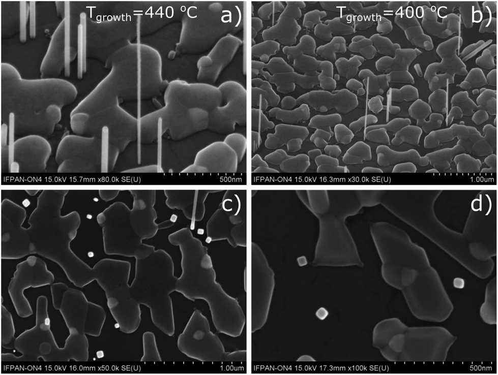 | ||
| Fig. 1 SEM images of Au-catalyzed SnTe nanowires deposited on graphene/SiC(6H) at 440 °C (a), (c); and at 400 °C (b), (d). Upper panels – sample plane tilted at 45° angle with respect to the e-beam direction; lower panels – sample plane perpendicular to the e-beam direction. Top of the NWs are visible in this projection as bright square-like objects. | ||
The majority of NWs visible in Fig. 1 are about 0.5 μm long and 50 nm thick; occasionally much longer and thinner NWs occur. Apparently, besides the SnTe NWs, the graphene/SiC substrate is also partially covered with planar SnTe. The Au nanocrystals which coagulate and do not catalyze SnTe NWs are visible as brighter spots on the irregular planar SnTe deposits. In spite of slightly lower surface NW densities there are no significant differences in the structure of both samples, but the planar MBE growth of SnTe is slightly more pronounced for sample (2) grown at a lower substrate temperature than sample (1).
SEM images taken with e-beam perpendicular to the substrate (parallel to the NWs) – Fig. 1c and d indicate that NWs have square cross sections, which correspond to the [001] NW growth axes. We have observed previously that, in contrast to III–V and II–VI semiconductor NWs which usually grow along the [111] crystallographic direction, the IV–VI NWs naturally grow along the [001] direction,25 which implies their 4-fold axial symmetry and square cross section.
In Fig. 1c and d it can be seen that there is lack of correlation of azimuthal orientation of the NWs. However almost all the NWs grow perpendicularly to the substrate. Fig. 2 shows the focused ion beam (FIB) cross-section acquired from sample (1). Two SnTe NWs embedded in a thick platinum layer can be identified in the image.
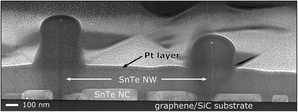 | ||
| Fig. 2 Low resolution TEM image of the focused ion beam cross-section of sample (1). The NWs are embedded in an electron deposited platinum layer. | ||
In the FIB cross-section, the blocks of planar SnTe nanocrystals (NC) are also visible. All the NCs have flat surfaces parallel to the interface plane (shown in more detail in Fig. 2). The two SnTe NWs indicated on the image are perpendicular to the substrate plane.
Fig. 3 shows the high resolution HRTEM image of the FIB cross-section of the SnTe/graphene/SiC hetero-interface (the same specimen measured in different zone axes). The negative spherical aberration imaging (NCSI) mode26 helps in visualizing the carbon atoms in SiC as well as in the graphene interlayer. With the spherical aberration correction settings used (Cs = −40 μm) the atomic columns in SiC and graphene appear bright against a darker background. Due to the low density of NWs we were unable to find a cross section with the SnTe(NW)/substrate interface in the specimen suitable for HRTEM investigations. Only planar SnTe NCs could be identified.
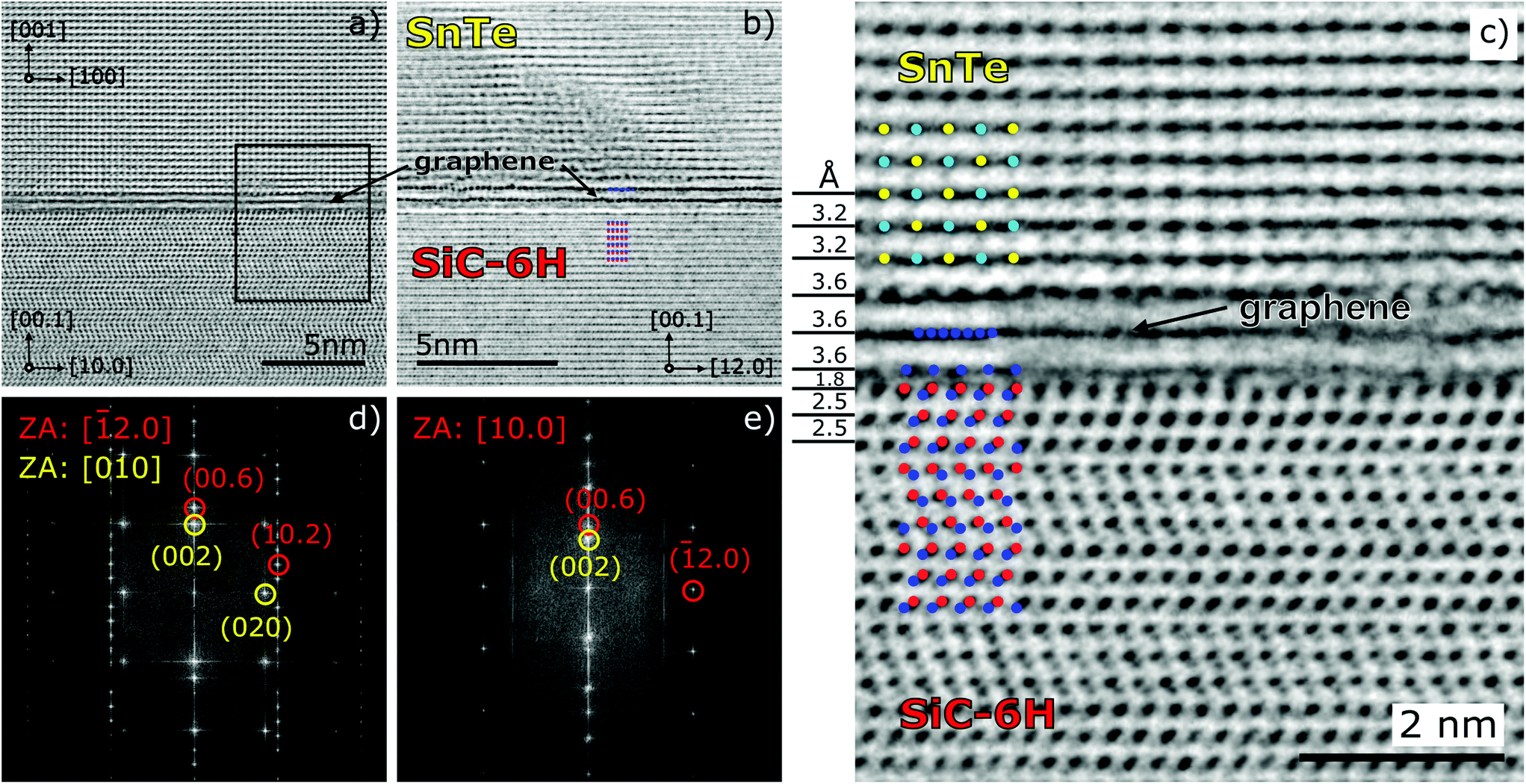 | ||
| Fig. 3 (a)–(c) Inverse contrast (atoms are black), NCSI high resolution TEM images of the SnTe/graphene/SiC(6H) interface. The positions of Si and C atoms in graphene/SiC are indicated by red and blue dots, respectively; whereas those of Sn, and Te in SnTe – by light-blue and yellow dots; (d) and (e) corresponding Fast Fourier Transform (FFT) images of the same region as shown in (c), with indexed FFT features originating from SiC(6H) (red) and SnTe (yellow). | ||
In the interface region with a graphene bi-layer we observe the distances between the lattice planes which differ from both SiC and SnTe (see Fig. 3c). Analyzing thoroughly the HRTEM image of this interface we can conclude that SiC is terminated by the carbon layer spaced 1.8 Å from the Si-plane of SiC(6H), similarly to that reported by Norimatsu and Kusunoki.27 Next we observe a distance of 3.6 Å between two graphene planes and the first monolayer of SnTe which is directly placed over the second layer of graphene. The SnTe crystal shown in Fig. 3 is slightly twisted around the [001] direction, so the atomic structure of SnTe is not perfectly resolved. The visible degradation of the graphene interlayer under an electron beam was detected after a 5 minute exposure to 300 kV electrons and total amorphization appeared after about 20 minutes under the normal HRTEM observation conditions at high magnification.
Even though the cross section shown in Fig. 3 applies to the interface between planar SnTe and the graphene/SiC(6H) substrate we believe that the interface between SnTe NW and graphene/SiC(6H) looks the same since similarly to planar SnTe NCs, the rock-salt SnTe NWs grow along the [001] direction. The planar growth of very thin SnTe (1 to 4 ML) on the graphene/SiC substrate has been investigated previously in the context of robust in-plane SnTe ferroelectric properties.28 The authors of ref. 28 also observed only the (001) orientation of thin SnTe islands deposited by MBE on graphene/SiC. On the other hand, for SnTe nanostructures (nanoplates and planar nanowires) deposited on silicon by the CVD technique, growth on both the (100) and (111) planes of SnTe has been observed.21
In spite of the dissimilarities between the (001) planes of cubic SnTe, with the 4-fold symmetry and the 6-fold symmetry of the graphene/SiC(6H) substrate there is some degree of correlation between SnTe(100) and graphene/SiC(6H), evidenced in the FFT features (see Fig. 3d). In the case of self-catalyzed GaAs NWs growth of graphene29 such correlation was even more pronounced and also concerned azimuthal correlations between GaAs NWs with the [111] growth axes and graphene, which is not observed in our case. For GaAs[111] NWs both the NWs and the substrate share common 6-fold symmetries, which do not occur for (001)SnTe and graphene/SiC(6H).
Fig. 4 shows the TEM images of a nanowire picked up from sample (2). It can be seen that the surface of the upper NW part (under the catalyst droplet) is smooth as opposed to the bottom where we observe pronounced surface roughness due to oxidation.
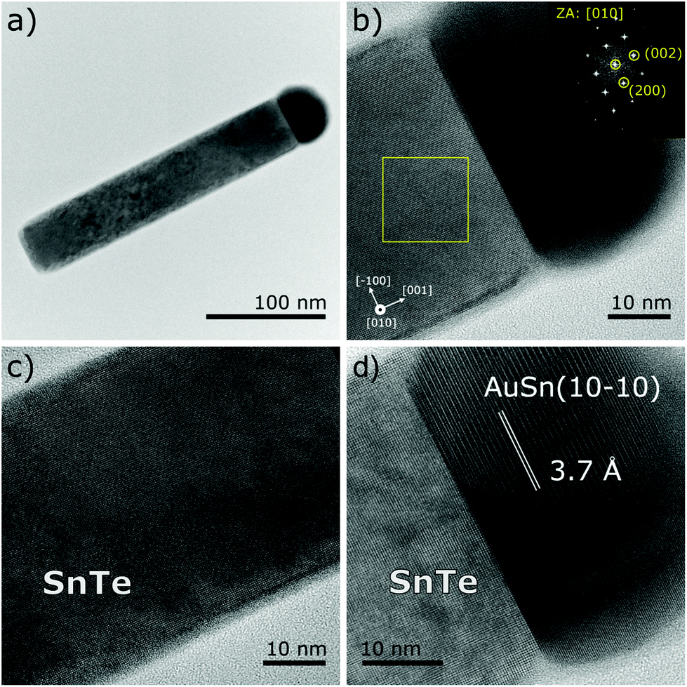 | ||
| Fig. 4 (a) Low resolution TEM image of a nanowire taken from sample (2); (b) high resolution image of the top nanowire part. The inset at the upper right corner shows 2D Fast Fourier Transform patterns taken from the region indicated by the yellow frame. The 4-fold symmetry FFT patterns correspond to the cubic rock-salt structure of the NW; (c) top part of the SnTe NWs below the catalyst nanocrystal, the scale bar corresponds to 10 nm; (d) the solidified droplet at the NW tip. | ||
The catalyst nanocrystal at the NW tip shown in Fig. 4d is inhomogeneous; the part visible in the upper section of the image is Sn-rich, as evidenced by the EDS composition scans described further in the text. The spacing between the crystallographic planes clearly visible in the upper part of the solidified droplet corresponds well to the 3.74 Å distance between the (10–10) planes of the hexagonal Au0.5Sn0.5 phase.30
As indicated above, the SnTe NWs with the [001] growth axes are totally free from structural defects. In the NWs shown in Fig. 4 and in many other NWs picked up from samples (1) and (2) the apparent inhomogeneity of the crystalline structure of a solidified catalyst droplet can be seen. The energy dispersion X-ray spectroscopy (EDS) elemental composition scans performed across the droplet (along the orange and blue lines shown in Fig. 5a) show that the larger part of the droplet is Sn-rich. The part of the solidified droplet represented with darker contrast in the TEM image is Sn rich, with the Sn content changing from 100% to 20% along the perpendicular scan line and from 60% to 30% along the parallel scan line. The scan directions are indicated by the arrows in Fig. 5a. In this part the atomic planes perpendicular to the NW axes could be identified (see Fig. 4).
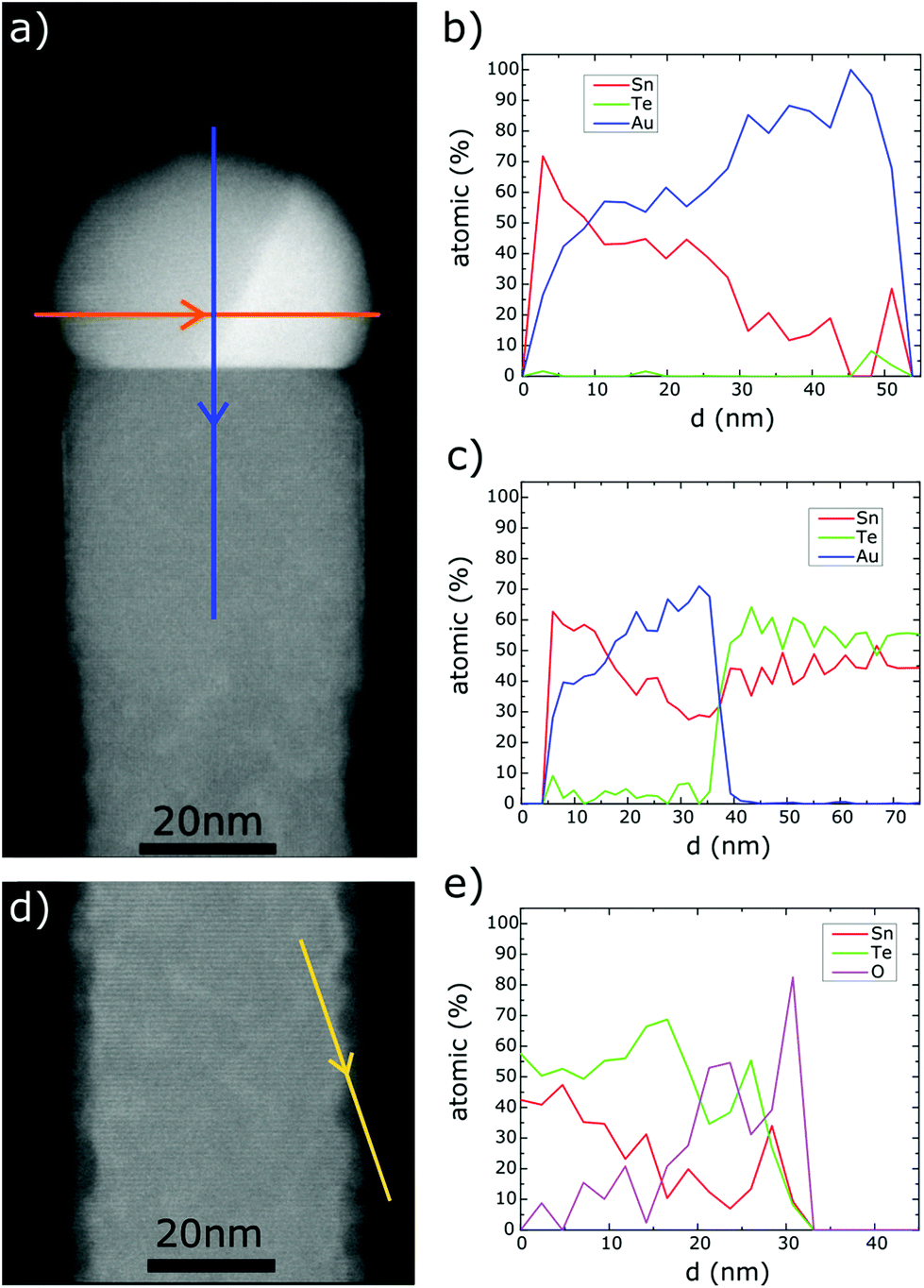 | ||
| Fig. 5 (a) STEM image of a solidified droplet at the SnTe nanowire tip. EDS elemental composition scans across (b) perpendicular and (c) parallel to the NW axis taken along the blue and orange arrows, respectively; (d) STEM image of the bottom part of the same NWs with the yellow arrow showing the EDS line scan across the sidewall of the NWs; (e) the elemental profiles of Sn, Te and O. | ||
A thorough inspection of the TEM images of the top part of SnTe NWs shown in Fig. 5 reveals that the NW sidewalls are oxidized (see the bottom part of Fig. 5a and d). Amorphous oxide is manifested by slightly darker contrast of the close-to-sidewall region, with respect to that of the NW body. It has also been confirmed by the EDS scan through this region (Fig. 5e). Apparently only the very top part of the NW down to about 40 nm below the interface with the catalyst droplet is free from oxidation. In some NWs this oxidation is very pronounced, but in all the cases the very top NW parts are protected against oxidation by a thin (2–3 ML) film of Au, or an Au–Sn alloy (this region is too thin to unequivocally determine its composition). The problem of SnTe oxidation has recently been investigated by Berchenko et al.31 The authors of ref. 31 show that the amorphous oxide at the SnTe(100) surfaces consists of a mixture of Sn and Te oxides and builds up during the first 10 minutes exposure of SnTe to air, then its thickness increases slowly in the time-scale of months, and can reach up to 20 nm after 1–2 years. In the NWs studied by us we have noticed different degrees of oxidation of NWs picked up from different samples, which have been stored in air for a similar time. We cannot directly infer what causes the differences in the oxidation rate; tentatively we attribute that to the different stoichiometries of SnTe NWs. An example of NW oxidation presented in Fig. 5d and the corresponding EDS profile (Fig. 5e) shows the significant contribution of oxygen at the sidewall. The sidewalls of the NWs collected from sample (1) grown at 440 °C are much more oxidized than those collected from sample (2), grown at 400 °C; and due to the known thermodynamic properties of SnTe32 we can infer that sample (1) is more Sn-rich than sample (2).
As can be seen in Fig. 5b and c the Au rich part of the droplet at the NW tip still contains a substantial amount of Sn. To identify which phase of the Au–Sn alloy is present in the droplet we have analyzed the two-dimensional Fast Fourier Transform (2D FFT) images of the different NW tip and droplet areas (see Fig. 6). The 2D FFT patterns obtained in three different zone axis directions correspond well to: Au0.5Sn0.5 – the main part of the droplet (light blue) and Au0.85Sn0.15 (red). The patterns corresponding to SnTe in the NW body are marked with yellow. Both Au–Sn intermetallic compounds are liquid at the SnTe NW growth temperature applied here (400 °C–440 °C),33 which indicates that the metal nanoparticle at the NW tip is in the liquid state during the NW growth.
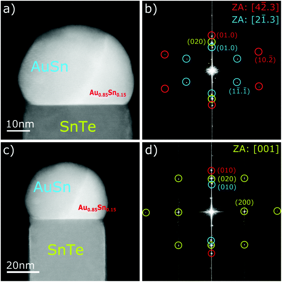 | ||
| Fig. 6 STEM-HAADF images – (a), (b) and corresponding 2D FFT images (c), (d) of different areas of the top part of SnTe nanowires in different zone axes: (c) [4−2.3] AuSn and [2−1.3] Au0.85Sn0.15, (d) [001] SnTe. The 2D FFT patterns corresponding to SnTe, Au0.5Sn0.5 and Au0.85Sn0.15 are marked with yellow, light blue and red colors, respectively. | ||
Fig. 7 shows two STEM-HAADF images of the SnTe NW grown on graphene/SiC collected from sample (3) grown at a substrate temperature of 450 °C for a much longer time (3 h) than samples (1) and (2), (1 h). Here the NWs are longer; however they have similar diameters as those picked up from samples (1) and (2) (see Fig. 1, 2 and 4) and are also totally free from structural defects across the whole NW lengths.
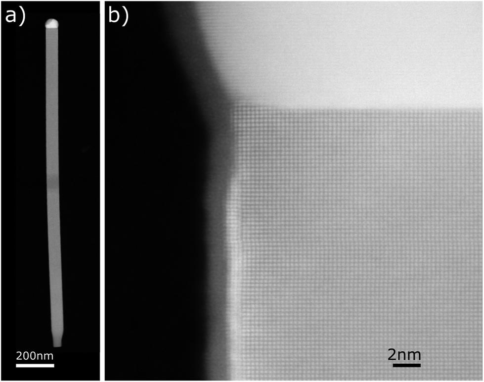 | ||
| Fig. 7 STEM-HAADF images of the same SnTe NW at different magnifications. | ||
Similarly to the NWs shown in Fig. 4–6, here the NW axis is also parallel to the SnTe[001] crystallographic direction. Likewise, the solidified metal droplet at the NW tip has an inhomogeneous composition.
As can clearly be seen in Fig. 7b the outer parts of the NW sidewall edges appear slightly brighter than the NW body (visible in all the SnTe NWs inspected by us). The EDS elemental composition scans of this region prove that similarly to the NWs shown in Fig. 4–6, in these regions the NW sidewalls are rich in gold and consist of a very thin (2–3 ML) film of gold or a gold–tin intermetallic alloy. As mentioned before, this very thin Au-rich shell prevents the SnTe NW sidewall from oxidation, which appears as light NW body narrowing visible in the lower part of the image shown in Fig. 5a.
Complementary information about the composition of the top part of SnTe NWs has been obtained by detection of plasmon resonances with the use of electron energy loss spectroscopy (EELS) in STEM. EELS is a powerful technique enabling the detection of electron energy losses due to excitation in a broad spectral range from optical energies up to vacuum ultraviolet.34Fig. 8 shows the 2D maps of EELS intensity obtained by the integration of signals for different energy window spectra of the SnTe NW tip and solidified Au–Sn droplet registered for the NWs shown in Fig. 7 (lower energy part of the EELS spectrum), and Sn and Te element distribution mapping due to the signal corresponding to the N4,5 edges of both elements. The plasmon-loss spectra are detected for energies corresponding to Au localized surface plasmons (2.4 eV),35 SnTe volume plasmons (14.8 eV) and SnTe surface plasmons (10.8 eV).36 The width of the EELS signal integration window was set at 1 eV, 3.4 eV and 3 eV, respectively.
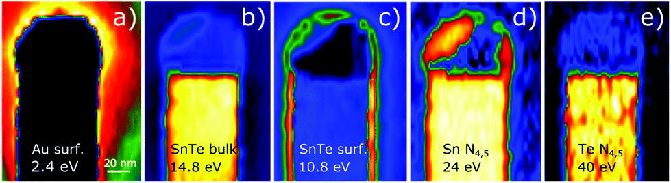 | ||
| Fig. 8 (a)–(c) Color coded maps of plasmon excitation of the top part of the SnTe nanowire detected by EELS. (a) Au surface plasmons (2.4 eV); (b) SnTe bulk plasmons (14.8 eV); (c) SnTe surface plasmons (10.8 eV); (d)–(e) color coded maps of the low loss edges of: (d) Sn N4,5 edge (24 eV), (e) Te N4,5 edge (40 eV) jump ratios visualizing distribution of Sn and Te in the top part of the SnTe nanowire. The spurious fluctuations of Sn and Te signals in panels (d) and (e) are experimental artifacts due to the low signal to noise ratios. | ||
In accordance with EDS and structural information obtained previously, the plasmon resonances observed in EELS confirm the presence of the thin Au-rich film at the top parts of the NW sidewalls. The higher energy part of the EELS spectrum (in the 20 eV–50 eV range) enables direct elemental mapping of the NWs and the metal catalyst at the top. The 2D mapping of the EELS signal corresponding to absorption at Sn N4,5 (24 eV) and Te N4,5 (40 eV) edges (see Fig. 8d and e) confirms the inhomogeneous composition of the catalyzing Au–Sn nanoparticles (solid at the TEM measurement temperature), and the negligible amount of Te in it.
4. Conclusions
In summary, we have investigated the Au-assisted MBE growth of SnTe topological crystalline insulator nanowires on graphene/SiC(6H) substrates. The NWs have a cubic rock-salt structure and grow along the [001] axes which implies their square cross-sections and occurrence of four {100} sidewalls recognized as topologically protected surfaces of the SnTe topological crystalline insulator. Analysis of the metal catalyst nanocrystals at the NW tips reveals that they contain a substantial amount of Sn. Two distinct phases of the Au–Sn intermetallic alloy: Au0.5Sn0.5 and Au0.85Sn0.15 have been identified in the solidified catalyst droplet. Both phases are liquid at the NW growth temperature (400 °C–440 °C) which indicates that the NWs grow in the VLS mode. In the majority of NWs, thoroughly investigated by TEM, no structural defects have been found along the entire NW lengths. In most of the NWs we observed the oxidation of the NW sidewalls. Only the very top parts of the NWs 40 nm–80 nm below the catalyzing metal nanoparticles are not oxidized due to protection by the very thin Au-rich film. This points out the necessity of depositing protective shells on the SnTe NW sidewalls in view of studying the transport phenomena involving charge carriers occupying topologically protected states residing at four SnTe(100) NW sidewalls.Conflicts of interest
There are no conflicts to declare.Acknowledgements
This work has been supported by the research projects no. 2014/13/B/ST3/04489, 2014/15/B/ST3/03833, 2016/21/B/ST5/03411, and 2017/25/N/ST5/02942 financed by the National Science Centre (Poland). The authors thank the Institute of Electronic Materials Technology and Dr W. Strupiński for graphene/SiC substrates.References
- S.-H. Wei and A. Zunger, Phys. Rev. B: Condens. Matter Mater. Phys., 1997, 55, 13605–13610 CrossRef CAS.
- D. Khokhlov, Lead Chalcogenides: Physics and Applications, Taylor & Francis, 2002 Search PubMed.
- L. Fu, Phys. Rev. Lett., 2011, 106, 106802 CrossRef PubMed.
- T. H. Hsieh, H. Lin, J. Liu, W. Duan, A. Bansil and L. Fu, Nat. Commun., 2012, 3, 982 CrossRef PubMed.
- P. Dziawa, B. J. Kowalski, K. Dybko, R. Buczko, A. Szczerbakow, M. Szot, E. Lusakowska, T. Balasubramanian, B. M. Wojek, M. H. Berntsen, O. Tjernberg and T. Story, Nat. Mater., 2012, 11, 1023 CrossRef CAS PubMed.
- S.-Y. Xu, C. Liu, N. Alidoust, M. Neupane, D. Qian, I. Belopolski, J. D. Denlinger, Y. J. Wang, H. Lin, L. A. Wray, G. Landolt, B. Slomski, J. H. Dil, A. Marcinkova, E. Morosan, Q. Gibson, R. Sankar, F. C. Chou, R. J. Cava, A. Bansil and M. Z. Hasan, Nat. Commun., 2012, 3, 1192 CrossRef PubMed.
- Y. Tanaka, Z. Ren, T. Sato, K. Nakayama, S. Souma, T. Takahashi, K. Segawa and Y. Ando, Nat. Phys., 2012, 8, 800 Search PubMed.
- Y. Tanaka, T. Shoman, K. Nakayama, S. Souma, T. Sato, T. Takahashi, M. Novak, K. Segawa and Y. Ando, Phys. Rev. B: Condens. Matter Mater. Phys., 2013, 88, 235126 CrossRef.
- K. Dybko, M. Szot, A. Szczerbakow, M. U. Gutowska, T. Zajarniuk, J. Z. Domagala, A. Szewczyk, T. Story and W. Zawadzki, Phys. Rev. B: Condens. Matter Mater. Phys., 2017, 96, 205129 CrossRef.
- A. A. Taskin, F. Yang, S. Sasaki, K. Segawa and Y. Ando, Phys. Rev. B: Condens. Matter Mater. Phys., 2014, 89, 121302 CrossRef.
- D. Zhang, H. Baek, J. Ha, T. Zhang, J. Wyrick, A. V. Davydov, Y. Kuk and J. A. Stroscio, Phys. Rev. B: Condens. Matter Mater. Phys., 2014, 89, 245445 CrossRef.
- C. M. Polley, V. Jovic, T.-Y. Su, M. Saghir, D. Newby, B. J. Kowalski, R. Jakiela, A. Barcz, M. Guziewicz, T. Balasubramanian, G. Balakrishnan, J. Laverock and K. E. Smith, Phys. Rev. B: Condens. Matter Mater. Phys., 2016, 93, 075132 CrossRef.
- I. Zeljkovic, D. Walkup, B. A. Assaf, K. L. Scipioni, R. Sankar, F. Chou and V. Madhavan, Nat. Nanotechnol., 2015, 10, 849 CrossRef CAS PubMed.
- D. Walkup, B. A. Assaf, K. L. Scipioni, R. Sankar, F. Chou, G. Chang, H. Lin, I. Zeljkovic and V. Madhavan, Nat. Commun., 2018, 9, 1550 CrossRef PubMed.
- X. Li and Q. Niu, Phys. Rev. B: Condens. Matter Mater. Phys., 2017, 95, 241411 CrossRef.
- S. Safaei, M. Galicka, P. Kacman and R. Buczko, New J. Phys., 2015, 17, 063041 CrossRef.
- K. Song, D. Soriano, A. W. Cummings, R. Robles, P. Ordejón and S. Roche, Nano Lett., 2018, 18, 2033–2039 CrossRef CAS PubMed.
- Z. Li, S. Shao, N. Li, K. McCall, J. Wang and S. X. Zhang, Nano Lett., 2013, 13, 5443–5448 CrossRef CAS PubMed.
- M. Safdar, Q. Wang, M. Mirza, Z. Wang, K. Xu and J. He, Nano Lett., 2013, 13, 5344–5349 CrossRef CAS PubMed.
- M. Safdar, Q. Wang, M. Mirza, Z. Wang and J. He, Cryst. Growth Des., 2014, 14, 2502–2509 CrossRef CAS.
- J. Shen, Y. Jung, A. S. Disa, F. J. Walker, C. H. Ahn and J. J. Cha, Nano Lett., 2014, 14, 4183–4188 CrossRef CAS PubMed.
- Y. Zou, Z. Chen, J. Lin, X. Zhou, W. Lu, J. Drennan and J. Zou, Nano Res., 2015, 8, 3011–3019 CrossRef CAS.
- M. d. l. Mata, X. Zhou, F. Furtmayr, J. Teubert, S. Gradecak, M. Eickhoff, A. Fontcuberta i Morral and J. Arbiol, J. Mater. Chem. C, 2013, 1, 4300–4312 RSC.
- W. Strupinski, K. Grodecki, A. Wysmolek, R. Stepniewski, T. Szkopek, P. E. Gaskell, A. Grüneis, D. Haberer, R. Bozek, J. Krupka and J. M. Baranowski, Nano Lett., 2011, 11, 1786–1791 CrossRef CAS PubMed.
- P. Dziawa, J. Sadowski, P. Dluzewski, E. Lusakowska, V. Domukhovski, B. Taliashvili, T. Wojciechowski, L. T. Baczewski, M. Bukala, M. Galicka, R. Buczko, P. Kacman and T. Story, Cryst. Growth Des., 2010, 10, 109–113 CrossRef CAS.
- C. L. Jia, L. Houben, A. Thust and J. Barthel, Ultramicroscopy, 2010, 110, 500–505 CrossRef CAS.
- W. Norimatsu and M. Kusunoki, Transitional structures of the interface between graphene and 6H-SiC (0 0 0 1), 2009, vol. 468, pp. 52–56 Search PubMed.
- K. Chang, J. Liu, H. Lin, N. Wang, K. Zhao, A. Zhang, F. Jin, Y. Zhong, X. Hu, W. Duan, Q. Zhang, L. Fu, Q.-K. Xue, X. Chen and S.-H. Ji, Science, 2016, 353, 274 CrossRef CAS PubMed.
- A. M. Munshi, D. L. Dheeraj, V. T. Fauske, D.-C. Kim, A. T. J. van Helvoort, B.-O. Fimland and H. Weman, Nano Lett., 2012, 12, 4570–4576 CrossRef CAS PubMed.
- N. Arora and B. R. Jagirdar, Phys. Chem. Chem. Phys., 2014, 16, 11381–11389 RSC.
- N. Berchenko, R. Vitchev, M. Trzyna, R. Wojnarowska-Nowak, A. Szczerbakow, A. Badyla, J. Cebulski and T. Story, Appl. Surf. Sci., 2018, 452, 134–140 CrossRef CAS.
- R. F. Brebrick and A. J. Strauss, J. Chem. Phys., 1964, 41, 197–205 CrossRef CAS.
- H. Okamoto and T. B. Massalski, Bull. Alloy Phase Diagrams, 1984, 5, 492 CrossRef.
- C. Colliex, M. Kociak and O. Stéphan, Ultramicroscopy, 2016, 162, A1–A24 CrossRef CAS PubMed.
- M. Bosman, V. J. Keast, M. Watanabe, A. I. Maaroof and M. B. Cortie, Nanotechnology, 2007, 18, 165505 CrossRef.
- R. F. Cook, Philos. Mag., 1971, 24, 1347–1353 CrossRef CAS.
| This journal is © The Royal Society of Chemistry 2018 |