
 Open Access Article
 This Open Access Article is licensed under a
 Creative Commons Attribution 3.0 Unported Licence
Plasmonic zero mode waveguide for highly confined and enhanced fluorescence emission†
Paolo
Ponzellini‡
,
Xavier
Zambrana-Puyalto‡
,
Nicolò
Maccaferri
 ,
Luca
Lanzanò
,
Francesco
De Angelis
and
Denis
Garoli
*
,
Luca
Lanzanò
,
Francesco
De Angelis
and
Denis
Garoli
*
Istituto Italiano di Tecnologia, Via Morego 30, 16163 Genova, Italy. E-mail: denis.garoli@iit.it
First published on 10th September 2018
Abstract
We fabricate a plasmonic nanoslot that is capable of performing enhanced single molecule detection at 10 μM concentrations. The nanoslot combines the tiny detection volume of a zero-mode waveguide and the field enhancement of a plasmonic nanohole. The nanoslot is fabricated on a bi-metallic film formed by the sequential deposition of gold and aluminum on a transparent substrate. Simulations of the structure yield an average near-field intensity enhancement of two orders of magnitude at its resonant frequency. Experimentally, we measure the fluorescence stemming from the nanoslot and compare it with that of a standard aluminum zero-mode waveguide. We also compare the detection volume for both structures. We observe that while both structures have a similar detection volume, the nanoslot yields a 25-fold fluorescence enhancement.
Introduction
Single-molecule fluorescence1–7 has been successfully applied to many areas of biomedicine, including DNA sequencing,8,9 diagnostics,10 and molecular biology.11 In particular, in the field of next generation sequencing (NGS), single molecule fluorescence detection is the technique at the core of commercially available devices.8,12,13 One of the most frequently used platforms for single molecule sequencing is based on zero-mode waveguides (ZMWs).14–16 These ZMWs consist of nanometric holes, usually fabricated in an aluminum film. The key design principle of a ZMW is a confined electromagnetic field at the bottom of the nanoholes. Given a certain illumination, the only molecules that feel the light field are the ones located at the bottom of the nanoholes. The rest of the molecules do not feel the light field, due to the screening of the metallic film. As a result, the only fluorophores that can be detected are the ones located in the tiny volume at the bottom of the hole. A ZMW reduces the detection volume by 3 to 6 orders of magnitude, from 10−15 (with a standard confocal microscope) to 10−18–10−21 liter, allowing for single-molecule detection.ZMWs of different shapes17–23 have been designed for single-molecule studies but in most of the cases the confined field at the bottom of the hole presents no significant enhancement. In contrast, optical nanoslots fabricated on Ag or Au films24–32 are known to provide both electric field and fluorescence enhancement (FE). Looking for a structure that combines the advantages of both the ZMWs and the optical nanoslots, Zhao and co-workers proposed an alternative solution.33 They designed a rectangular optical hollow nanoslot on a bilayer of consecutive gold and aluminum films. Then, they theoretically demonstrated that the bilayer configuration replicates the field confinement obtained in aluminum ZMWs but with a significant light field enhancement. That is, these nanoslots conjugate the advantages of a ZMW with those of a plasmonic slot: they behave as plasmonic ZMWs. On the one hand, the noise is reduced by avoiding the excitation of molecules that are not at the bottom of the plasmonic ZMW. On the other hand, a hotspot at the bottom of the slot enhances the absorption of the fluorescent molecules in that region.
Inspired by the design proposed by Zhao et al.,33 we have fabricated bilayer nanoslots on a Au–Al substrate. We have simulated their behavior under a plane wave excitation, and we have experimentally measured their FE as well as their detection volume. We have observed that the fabrication of the plasmonic ZMW proposed by Zhao et al.33 is challenging with standard nanofabrication tools. We did not manage to fabricate plasmonic ZMWs with vertical walls. Instead, the walls of the slot had a flared shape. We have theoretically verified that the flared shape red-shifts the spectral behavior of the slot. Then, we have characterized the plasmonic ZMW using fluorescence correlation spectroscopy (FCS). Compared to the confocal volume, we have measured a reduction of the detection volume by a factor 105. This detection volume reduction allows for a fluorescence detection at the single molecule level with μM concentrations, which are typical of many biological phenomena.34 Still using FCS, we have obtained a 25-fold FE for an illumination wavelength of 676 nm, the wavelength for which our ideal structures are theoretically optimized.
The outlined results demonstrate that the proposed design improves the performance of ZMWs for fluorescence spectroscopy at the single molecule level. Furthermore, the spectral simulations suggest that the plasmonic ZMW has a broadband behavior, thus making it useful for multiple colors applications, such as FRET spectroscopy.35
Results and discussion
The experimental verification of the design proposed by Zhao et al.33 (Fig. 1a) started with the fabrication of the two structures: a standard Al ZMW and a bilayer Au–Al nanoslot. The preparation of 40 nm wide structures into a 150 nm thick metallic film can be done following different strategies such as electron beam lithography and lift-off, or direct milling of the structure by means of focused ion beam (FIB). We have not used the first method, since it presents some difficulties during the lift-off process, due to the high transverse aspect-ratio and the small dimensions of the structures. Instead, FIB allows for a rapid preparation of the nanoslots by directly milling into the bilayer film. An intrinsic drawback of FIB milling is the unavoidable flared shape of the fabricated slots. The two cross sections depicted in Fig. 1(b and d) show this phenomenon for the two fabricated structures. A second issue related to FIB regards the milling depth. The milling time needs to be well calibrated to prevent the FIB ions from damaging the glass underneath the sample. Several cross sections with various milling parameters were performed for calibrating the milling time. These cross sections also allowed us to come up with the correct design dimensions for the transverse section. Once the milling parameters were calibrated, we searched for the best performing nanoslots and ZMWs. For this purpose, we fabricated (and measured, as described below) parametric samples, with Au–Al nanoslots and Al ZMWs of various dimensions. The results of this optimization are summarized below (see Fig. 4). The details of the fabrication process by means of FIB are reported in Methods, while the actual shape of the milled structures is shown in Fig. 1(a – inset and c).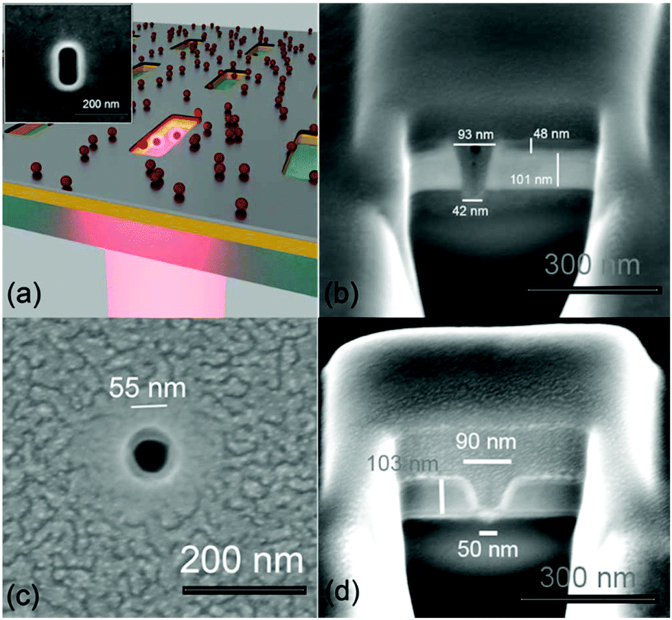 | ||
| Fig. 1 SEM images of the fabricated structures. (a) Schematic illustration of the Au–Al nanoslots; Inset: SEM micrograph of a fabricated nanoslot; (b) gold–aluminum nanoslot, cross section. A 101 nm gold layer and a 48 nm aluminum layer are visible. For realizing a cleaner and more vertical cross section after the FIB milling, a platinum layer was deposited above the nanostructures: it is the rough material visible in the two cross sections, above the layers and inside the slot. (c) Aluminum ZMW, top view. (d) Aluminum ZMW, cross section. The 103 nm thick aluminum layer is clearly visible, as well as the platinum layer above. | ||
We also fabricated Ag–Al nanoslots to benefit from the plasmonic properties of silver (Ag). However, we observed that the Ag–Al bi-layer was unstable when it got in contact with the fluorophore solution, thus preventing us from doing consistent measurements.
The details about the Ag–Al nanoslot design, fabrication and measurements issues are given in the ESI.† In Fig. 2, we compare the ZMWs that have been fabricated for this work, and the ideal-type of structures reported in ref. 33. The simulations in ref. 33 regard ideal structures, with vertical walls. Here we consider geometric configurations with both vertical and tilted walls.
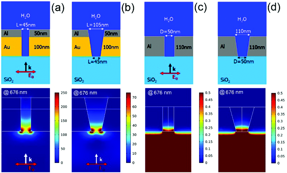 | ||
| Fig. 2 Sketch of a section of the ideal and fabricated rectangular Au–Al (top panels a–b) and of the circular Al (top panel c–d) nanoslot. Near-field intensity distributions of the Au–Al (bottom panels a–b), and Al nanoslots (bottom panels c–d) (ideal and fabricated) at the experimental wavelength. The maximum of the colorbar does not correspond to the field maximum. The section planes of the rectangular slots are parallel to the short axis. | ||
The latter configuration, as previously reported, models the fabricated structures with the FIB. Both the ideal and fabricated geometries are shown in the top panels of Fig. 2a–d for the rectangular Au–Al and circular Al ZMWs respectively.
In the bottom panels of Fig. 2a–d we depict the near-field intensity distribution for the ideal and fabricated Au–Al and Al ZMWs. Notice that all the images are saturated. The colorbar of each intensity distribution is chosen to render the field-distribution understandable. The field distributions have been obtained at 676 nm, since it is the wavelength at which the experiments have been performed and it is very close to the resonance of the ideal structure (680 nm). All near-field distributions have been obtained using a plane wave excitation, with a polarization parallel to the minor axis of the structure. It is observed that both the Au–Al and the Al ZMWs confine the field at the bottom of the nanohole. While the Al ZMW does not produce any field enhancement (to be noted that with larger diameter a Al ZMW can provide slightly higher field intensity27), the ideal Au–Al nanoslots yield a maximum intensity enhancement above 250 at the bottom of the slot. In contrast, the fabricated structure features a maximum field enhancement above 75 at the bottom of the slot. These values are related to the absorption enhancement of a fluorescent probe-molecule that freely diffuses into the considered nanostructures. In the ESI† we show that a field enhancement above 120 can be obtained with Ag–Al nanoslots.
Typically, several dyes (emitting at different wavelengths) are used in sequencing applications.8,12,36 The same holds for FRET, where the donor and the acceptor have different excitation and emission wavelengths.37 Hence a plasmonic platform that is capable of enhancing the fluorescence signal in a broadband energy range could be extremely useful. In the light of this, in Fig. 3 we have computed the average near-field intensity enhancement as a function of the wavelength for the two ZMWs in consideration (see ESI† for the case of Ag–Al). The computation is done at the glass/water interface, i.e. at the bottom of the ZMW.
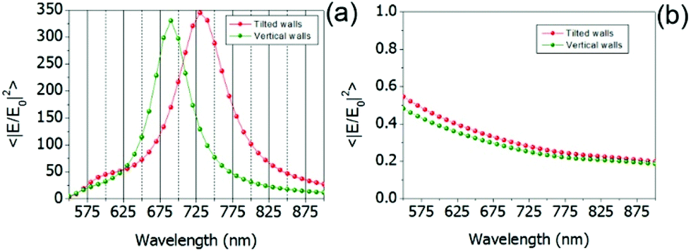 | ||
| Fig. 3 Calculated field enhancements, averaged on the glass/water interface at the bottom of the two nanostructures. (a) Average field enhancement for the rectangular ideal (green) and fabricated (red) Au–Al nanoslot. (b) Average field enhancement for the rectangular ideal (green) and fabricated (red) Al ZMWs. | ||
The excitation is a unitary plane wave, polarized along the minor axis of the structure, within the spectral range between 550 and 900 nm. Similarly to Fig. 2, both the ideal and the fabricated structures are simulated. Looking at the results in Fig. 3, it is clear that the flared shape of the ZMWs needs to be taken into account. Even if the qualitative behavior of both structures is the same, the red-shifted resonant behavior of the flared structure has some important quantitative effects. In particular, it decreases the average near-field intensity enhancement of the ideal plasmonic ZMW from 300 to 100 at 676 nm.
In order to verify the behavior of the plasmonic ZMWs, we have performed FCS measurements using a solution of Alexa Fluor 680 dye in water. We have excited the dyes at 676 nm, which was the closest wavelength to the Au–Al ZMW spectral maximum that was available for us (see Methods). Note that water has a relatively large surface tension. As a consequence, we realized that an oxygen plasma cleaning of the surface had to be performed on every sample before dropping the fluorophore solution on top of the nanoslots. Oxygen makes the metallic surface hydrophilic, allowing the fluorophore solution to enter the nanometric nanoslots. The details about the plasma treatment and the optical measurements can be checked in the Methods.
Now, the use of the FCS technique allows us to characterize each structure by evaluating the reduction of the detection volume (VR), as well as fluorescence enhancement. Both the VR and the FE are normalized with respect to the values obtained for a solution of Alexa Fluor 680 on a cover glass. In the following, we will refer to the measurements on a cover glass as the confocal measurements. The confocal measurements have been performed with two different concentrations (C) of the dyes. For each measurement, the temporal correlation of the fluorescent signal is measured as G(τ) = 〈F(t)F(t + τ)〉/〈F(t)〉2, where F(t) is the fluorescence signal, τ is the lag time and 〈〉 indicates time averaging.38 We fitted the data using a two dimensional Brownian diffusion model (see Methods), obtaining the average number of molecules N and the average diffusion time τd.38 Then, we computed the count rate per molecule (CRM) as CRM = 〈F〉/N, and the detection volume as DV = N/C. The confocal results are summarized in Table 1.
| C (nM) | CRM (kHz) | N | DV (p./nM) |
|---|---|---|---|
| 0.86 | 2.0 ± 0.9 | 2.1 | 2.41 |
| 8.6 | 2.3 ± 0.6 | 23 | 2.67 |
The CRM is given in thousands of counts per second (kHz) and the DV is in particles per nM. As expected, CRM and DV do not vary with the concentration, therefore we averaged out the results to obtain the values in Table 2.
| CRM (kHz) | DV (p./nM) |
|---|---|
| 2.1 ± 0.5 | 2.54 ± 0.13 |
For our nanostructures, the VR and the FE of a slot (or ZMW) “i”, were obtained as VRi = DVconf/DVi and FEi = CRMi/CRMconf, respectively. As mentioned above, we have fabricated several Au–Al slots with different sections and volumes. Using FCS, we have characterized each slots in terms of its FE and DV. We define each slot by the FIB software parameters that have been used to fabricate the slots.
Three parameters are given concerning three different dimensions (x,y,z). x–y are related to the transverse section of the slot, and z to the milling time and hence to the depth of the structure. In order to compare the behavior of the different slots, we compute two parameters, the transverse section area TS = x·y (nm2), and the volume V = x·y·z (nm3). In Fig. 4, we show two graphs, where the FE of each slot is plotted as a function of TS and V. We observed that the nanoslot with FIB software dimensions (60, 130, 30) nm clearly out-performs the rest, hence we decided to use it in the fluorescence experiments.
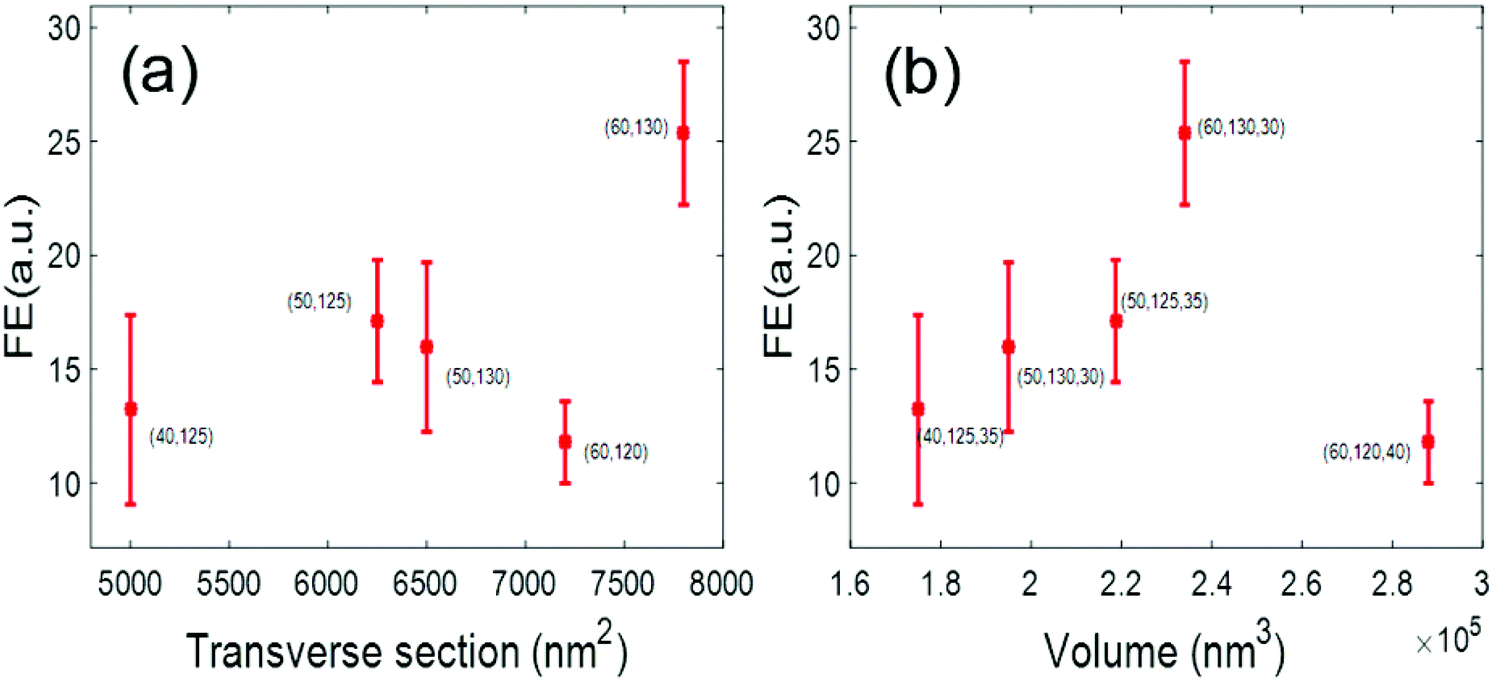 | ||
| Fig. 4 Fluorescence enhancement measurements with Au–Al nanoslots. (a) Fluorescence enhancement as a function of the theoretical transverse section of the slot. (B) Fluorescence enhancement as a function of the theoretical volume of the slot. All experiments have been done using a concentration of using of Alexa Fluor 680 of 34 μM. | ||
According to our cross sections (see Fig. 1a), the FIB z parameter (30 nm) corresponds to milling the two metallic layers without significantly affecting the glass substrate, whereas the (60![[thin space (1/6-em)]](https://www.rsc.org/images/entities/char_2009.gif) 130) nm transverse parameters yield a nanoslot with an actual transverse section of about 45 × 115 nm2 at the water–glass interface. Notice that these dimensions almost match the optimized 40 × 110 nm dimensions reported in ref. 33. As for the Al ZMWs, we have observed that they had an optimum§ behavior when their dimensions were set to (D,z) = (60,70) nm in the FIB software design. According to our cross sections (see Fig. 1c), these parameters correspond to milling the Al layer until digging the glass substrate for few nanometers, yielding a hole of about 50 nm of diameter at the bottom.
130) nm transverse parameters yield a nanoslot with an actual transverse section of about 45 × 115 nm2 at the water–glass interface. Notice that these dimensions almost match the optimized 40 × 110 nm dimensions reported in ref. 33. As for the Al ZMWs, we have observed that they had an optimum§ behavior when their dimensions were set to (D,z) = (60,70) nm in the FIB software design. According to our cross sections (see Fig. 1c), these parameters correspond to milling the Al layer until digging the glass substrate for few nanometers, yielding a hole of about 50 nm of diameter at the bottom.
A summary of our FCS measurements for the optimized structures is displayed in Fig. 5. In Fig. 5a, we display representative fluorescence traces for the Alexa Fluor 680 freely diffusing into the Al ZMWs, the Au–Al nanoslots, and the confocal configuration. In Fig. 5b, we plot the autocorrelation function G(τ) associated to each of the fluorescence traces. As expected, we observe that the Al and Au–Al ZMWs can be used at concentrations of the order of tens of μM and still perform single molecule detection. In Table 3, we summarize the behavior of the Al and Au–Al nanostructures.
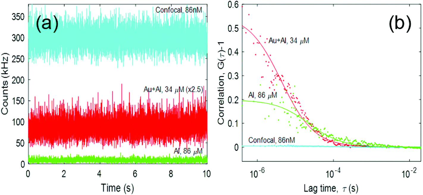 | ||
| Fig. 5 FCS measurements in Au–Al and Al ZMWs, as well as confocal reference. (a) Fluorescence time traces of representative samples. Note that the Au–Al counts have been multiplied times 2.5 for displaying purposes (b) FCS correlation function (dots, raw data; lines, numerical fits). The cyan traces refer to the confocal reference with a concentration of 86 nM of Alexa Fluor 680; the green traces are obtained with an Al ZMW with a diameter of 60 nm and a depth of 70 nm, using a concentration of 86 μM; the red traces are obtained with an optimized Au–Al ZMW at a concentration of 34 μM. | ||
| Nanostructure | FE (a.u.) | VR (a.u.) |
|---|---|---|
| Al | 1.3 ± 0.5 | 120000 ± 10000 |
| Au + Al | 25 ± 3 | 110000 ± 40000 |
The FE of the Au–Al ZMW with respect to the confocal case is 25, and the detection volume has been reduced by 5 orders of magnitude. The diffusion time of the dyes was also reduced. We observed a 20-fold reduction in the diffusion time, which is consistent with some of the values reported in the literature.39 We also observe that the FE of the Au–Al slot is 25 times greater than that of the Al ZMW. Furthermore, its detection volume is comparable to the volume of the Al ZMW. Both features make the fabricated Au–Al ZMWs good candidates for performing single molecule detection.
Last but not least, it is worth noticing that the intensity enhancement obtained in the electromagnetic simulations cannot be directly related to the expected experimental FE. There are various reasons for that. In the first place, an increase in the field enhancement at the excitation wavelength is related to an increase in the absorption of the molecules. Nonetheless, this relation is not linear.39 The absorption of the dyes saturates at a certain excitation power. Given that the CRM of the Alexa Fluor 680 dyes in the confocal configuration is already 2.1 ± 0.3, it is likely that the dyes behave non-linearly if the intensity is enhanced by a factor 100. In the second place, the intensity enhancement simulated in Fig. 2 and 3 does not correspond to the real intensity enhancement that the dyes feel in the experiment.
This is due to the fact that the experimental excitation is not a plane wave. The excitation beam is a tightly focused (the microscope objective has a NA = 1.49) Gaussian beam. The tightly focused beam must be taken into account in order to compute the theoretical increase in the absorbance of the molecules. In the ESI† we show the near-field intensity enhancement of the ideal Au–Al ZMW excited by a Gaussian beam focused down to a spot of 500 nm. It is observed that the intensity enhancement is significantly reduced. Anyway, in a real application of this platform, this is not big issue cause a weakly focused laser beam is typically used to illuminate hundreds of ZMWs for parallel detection. Therefore, the large field enhancement should be still well maintained. In the third place, our fluorescence measurements are the result of the dipolar emission of Alexa Fluor 680 dyes in a tiny ZMW. The enhancement of the spontaneous emission of dyes, also known as Purcell factor, does not depend on the field enhancement, but rather on the orientation of the dipoles and the environment surrounding them.40 That is, the enhancement of the spontaneous emission rate cannot be estimated with a near-field calculation. Furthermore, the Alexa Fluor 680 dyes have a quantum yield of approximately 0.36, which means that their emission cannot be increased more than three times. Obtaining huge fluorescence enhancements is easier when dyes with a very low quantum yield are used.28 Finally, the presence of a Ti adhesion layer on the glass substrate (see methods section) also impact on the expected field enhancement as illustrated in ESI.† Nevertheless, despite all the differences, we still have observed a significant resemblance between the near-field intensity enhancement computed in Fig. 2 and 3, and the FE measurements summarized in Table 3.
Conclusions
We have reported on the fabrication of bilayer nanoslots on a Au–Al substrate. The fabrication of the nanoslots has turned out to present some challenges with standard nanofabrication tools. We did not manage to fabricate plasmonic ZMWs with flat walls. Instead, the walls of the fabricated slots have a pyramidal shape. We have simulated both the ideal and the fabricated structures and compared their near-field intensity enhancement as well as their spectral properties. The simulations suggest that the Au–Al nanoslots could be used in broadband applications. Finally, we have characterized the structures by means of their fluorescence enhancement and the reduction of their detection volume. We have measured a reduction of the detection volume by a factor 105, as well as a fluorescence enhancement of 25. These features demonstrate that the fabricated Au–Al nanoslots improve the performance of ZMWs for fluorescence spectroscopy at the single molecule level. Furthermore, given that the spectral simulations show that our plasmonic ZMWs have a broadband behavior, we believe that it could be of great interest for sequencing purposes, where FRET and multiple colors approaches can find an application.Methods
Sample fabrication
A 150 μm thick glass slide is used as the substrate. Firstly, the substrates have been thoroughly cleaned in order to obtain a smooth metallic surface with the subsequent metal deposition. The substrates have been sonicated in acetone and isopropanol, washed in a piranha solution (3::2 H2SO4::H2O2) and thoroughly rinsed in deionized and milliq water. The metal layers have been deposited by means of electron-beam evaporation in high-vacuum. A 3 nm Titanium layer has been used in all the metal configurations to link the glass substrate with the metallic layers above. This passage has been found to be critical for avoiding the delamination of the metallic layers once in contact with the fluorophore solution. We expect that such a thin layer of Titanium slightly affect the optical properties of our structures (details in ESI†). Titanium has been evaporated at the rate of 0.3 Å s−1. In the aluminum ZMW case, a 110 nm aluminum layer has been evaporated, at a deposition rate of 1.5 Å s−1. In the gold/aluminum ZMW case, a 100 nm layer of gold has been evaporated at the rate of 0.3 Å s−1 and a 50 nm aluminum layer has been evaporated at 1.5 Å s−1.
In the silver/aluminum ZMW case (see ESI†), a 100 nm layer of silver has been evaporated at the rate of 1 Å s−1 and a 50 nm aluminum layer has been evaporated at 1.5 Å s−1.
The bilayer is drilled by means of a gallium FIB at an accelerating bias of 30 kV, with a dwell time of 1 μs, and with the ionic current set to a low value (7.7 pA) in order to obtain a tiny beam and hence narrow structures. Due to the high aspect ratio of our structures, the actual inner shape of the nanoslots is not visible by mean of a top view SEM image. Only the upper, external shape of the nanoslot, at the aluminum–water interface, results clearly visible and measurable. For evaluating the milling parameters, both in the vertical and horizontal planes, several cross sections have been realized on trial slots on every fabricated sample (Fig. 1a and c). First of all, this approach allowed us to calibrate the milling time, in order to reach the glass substrate below the metallic layer, without digging into the glass. In the second place, it allowed us to measure the resulting slope of the nanoslot walls. This way we could calibrate the design of the nanoslot within the FIB software in order to obtain the desired rectangular shape with the optimal simulated dimensions, at the nanoslot bottom interface. Starting from those parameters we have fabricated parametric samples where the nanoslots have various dimensions, in a range centered around the simulated dimensions. We have followed the same strategy for the Al ZMWs.
Once milled, the samples have been stored in a nitrogen atmosphere to avoid deterioration.
Before the fluorescence measurements, a 90 seconds oxygen plasma (100% O2; 100 W) was performed on the samples, to make the surface hydrophilic, and hence to allow the water into the nanoslots.
Optical measurements
The experiments are performed on an inverted microscope with an oil-immersion 1.49NA microscope objective. The light beam, which enters the microscope through its rear port, is obtained with a continuous ArKr gas laser operating at λ = 676 nm. Our ArKr laser has many available lines, and λ = 676 nm is the longest one. Before arriving in the microscope, the beam is filtered by a bandpass filter 676/29 nm. The power of the laser before entering the rear port of the microscope is 15 μW. The samples that we use for the experiment are held on a sample holder, which is attached to a micro and a nanopositioner. The nanopositioner is used to center the sample with respect to the incident beam. The nanopositioner is also used to place the sample at the z plane where the fluorescence counts are maximized. A 60 μL droplet of an Alexa Fluor 680 solution is placed onto the sample. The dyes freely diffuse into the nanostructures. Three filters are used to separate the fluorescence of the dyes from the light reflected off the sample. The filters are a dichroic mirror at 685 nm, a longpass filter at 685 nm, and a bandpass filter at 711/25 nm. After the bandpass filter, a 50/50 beam splitter is used to split the fluorescence light signal into two different channels. Then, two 50 mm lenses are used to focus the fluorescence signal onto two equivalent avalanche photodiodes (APD). The signal of the APDs is recorded with a time-correlated single photon counting module. The fluorescence trace duration is typically 1 minute, with a binning time of 200 ns. After the detection of the fluorescence trace, three different calculations are carried out to be able to retrieve the count rate per molecule (CRM). First, the signals measured by the two APDs are correlated. A 2D translational diffusion model is used to fit the correlation function and obtain the average number of molecules 〈N〉.38 This is a valid approximation of a 3D diffusion model when of the axial size of the observation volume is much larger than its lateral.41 Second, the average of the fluorescence trace 〈F〉 and its standard deviation δF are calculated. Finally, the CRM is obtained as CRM = 〈F〉/〈N〉 ± δF/〈N〉. This operation is performed several times, and the final CRM is obtained as an average of the different CRM measurements for each slot.Numerical simulations
Numerical simulations based on the Finite-Element Method implemented in the RF Module of Comsol Multiphysics® were carried out to investigate the electromagnetic response of an isolated plasmonic ZMW. The dimensions of the simulated ZMWs were set according to the average sizes obtained from SEM investigations. A dielectric constant n = 1.33 was used for water, and n = 1.5 was set for the glass substrate. The refractive indexes of Au, Ag and Al were taken from Rakic.42 The model computes the electromagnetic field in each point of the simulation region, enabling the extraction of the quantities plotted along the manuscript. The unit cell was set to be 250 nm wide in both x- and y-directions and 1000 nm along the z-direction, with perfect matching layers (150 nm thick) at the borders. A linearly polarized plane wave impinges on the structure from the water side, with the electric field aligned along the short axis of the ZMW.Conflicts of interest
There are no conflicts to declare.Acknowledgements
The research leading to these results has received funding from the Horizon 2020 Program, FET-Open: PROSEQO, Grant Agreement no. [687089]. X. Z.-P. wants to thank Assegid M. Flatae, Francesco Tantussi, Marti Duocastella and Juan De Torres for interesting discussions.Notes and references
- M. Wanunu, T. Dadosh, V. Ray, J. Jin, L. McReynolds and M. Drndić, Nat. Nanotechnol., 2010, 5, 807–814 CrossRef PubMed.
- W. Li, N. A. W. Bell, S. Hernández-Ainsa, V. V. Thacker, A. M. Thackray, R. Bujdoso and U. F. Keyser, ACS Nano, 2013, 7, 4129–4134 CrossRef PubMed.
- A. McMullen, H. W. De Haan, J. X. Tang and D. Stein, Nat. Commun., 2014, 5, 4171 CrossRef PubMed.
- C.-H. ZHANG, G.-J. LI and J.-H. WANG, Chin. J. Anal. Chem., 2014, 42, 607–615 Search PubMed.
- P. Zijlstra, P. M. R. Paulo and M. Orrit, Nat. Nanotechnol., 2012, 7, 379–382 CrossRef PubMed.
- M. S. Alam, F. Karim and C. Zhao, Nanoscale, 2016, 8, 9480–9487 RSC.
- F. Karim, T. B. Smith and C. Zhao, J. Nanophotonics, 2017, 12, 012504 CrossRef.
- J. Eid, A. Fehr, J. Gray, K. Luong, J. Lyle, G. Otto, P. Peluso, D. Rank, P. Baybayan, B. Bettman, A. Bibillo, K. Bjornson, B. Chaudhuri, F. Christians, R. Cicero, S. Clark, R. Dalal, A. DeWinter, J. Dixon, M. Foquet, A. Gaertner, P. Hardenbol, C. Heiner, K. Hester, D. Holden, G. Kearns, X. Kong, R. Kuse, Y. Lacroix, S. Lin, P. Lundquist, C. Ma, P. Marks, M. Maxham, D. Murphy, I. Park, T. Pham, M. Phillips, J. Roy, R. Sebra, G. Shen, J. Sorenson, A. Tomaney, K. Travers, M. Trulson, J. Vieceli, J. Wegener, D. Wu, A. Yang, D. Zaccarin, P. Zhao, F. Zhong, J. Korlach and S. Turner, Science (80-.), 2009, 323, 133–138 CrossRef PubMed.
- S. Uemura, C. E. Aitken, J. Korlach, B. A. Flusberg, S. W. Turner and J. D. Puglisi, Nature, 2010, 464, 1012–1017 CrossRef PubMed.
- M. Pitschke, R. Prior, M. Haupt and D. Riesner, Nat. Med., 1998, 4, 832–834 CrossRef PubMed.
- K. Bacia, S. A. Kim and P. Schwille, Nat. Methods, 2006, 3, 83–89 CrossRef PubMed.
- D. R. Bentley, S. Balasubramanian, H. P. Swerdlow, G. P. Smith, J. Milton, C. G. Brown, K. P. Hall, D. J. Evers, C. L. Barnes, H. R. Bignell, J. M. Boutell, J. Bryant, R. J. Carter, R. Keira Cheetham, A. J. Cox, D. J. Ellis, M. R. Flatbush, N. A. Gormley, S. J. Humphray, L. J. Irving, M. S. Karbelashvili, S. M. Kirk, H. Li, X. Liu, K. S. Maisinger, L. J. Murray, B. Obradovic, T. Ost, M. L. Parkinson, M. R. Pratt, I. M. J. Rasolonjatovo, M. T. Reed, R. Rigatti, C. Rodighiero, M. T. Ross, A. Sabot, S. V. Sankar, A. Scally, G. P. Schroth, M. E. Smith, V. P. Smith, A. Spiridou, P. E. Torrance, S. S. Tzonev, E. H. Vermaas, K. Walter, X. Wu, L. Zhang, M. D. Alam, C. Anastasi, I. C. Aniebo, D. M. D. Bailey, I. R. Bancarz, S. Banerjee, S. G. Barbour, P. A. Baybayan, V. A. Benoit, K. F. Benson, C. Bevis, P. J. Black, A. Boodhun, J. S. Brennan, J. A. Bridgham, R. C. Brown, A. A. Brown, D. H. Buermann, A. A. Bundu, J. C. Burrows, N. P. Carter, N. Castillo, M. C. E. Catenazzi, S. Chang, R. Neil Cooley, N. R. Crake, O. O. Dada, K. D. Diakoumakos, B. Dominguez-Fernandez, D. J. Earnshaw, U. C. Egbujor, D. W. Elmore, S. S. Etchin, M. R. Ewan, M. Fedurco, L. J. Fraser, K. V. Fuentes Fajardo, W. Scott Furey, D. George, K. J. Gietzen, C. P. Goddard, G. S. Golda, P. A. Granieri, D. E. Green, D. L. Gustafson, N. F. Hansen, K. Harnish, C. D. Haudenschild, N. I. Heyer, M. M. Hims, J. T. Ho, A. M. Horgan, K. Hoschler, S. Hurwitz, D. V. Ivanov, M. Q. Johnson, T. James, T. A. Huw Jones, G. D. Kang, T. H. Kerelska, A. D. Kersey, I. Khrebtukova, A. P. Kindwall, Z. Kingsbury, P. I. Kokko-Gonzales, A. Kumar, M. A. Laurent, C. T. Lawley, S. E. Lee, X. Lee, A. K. Liao, J. A. Loch, M. Lok, S. Luo, R. M. Mammen, J. W. Martin, P. G. McCauley, P. McNitt, P. Mehta, K. W. Moon, J. W. Mullens, T. Newington, Z. Ning, B. Ling Ng, S. M. Novo, M. J. O'Neill, M. A. Osborne, A. Osnowski, O. Ostadan, L. L. Paraschos, L. Pickering, A. C. Pike, A. C. Pike, D. Chris Pinkard, D. P. Pliskin, J. Podhasky, V. J. Quijano, C. Raczy, V. H. Rae, S. R. Rawlings, A. Chiva Rodriguez, P. M. Roe, J. Rogers, M. C. Rogert Bacigalupo, N. Romanov, A. Romieu, R. K. Roth, N. J. Rourke, S. T. Ruediger, E. Rusman, R. M. Sanches-Kuiper, M. R. Schenker, J. M. Seoane, R. J. Shaw, M. K. Shiver, S. W. Short, N. L. Sizto, J. P. Sluis, M. A. Smith, J. Ernest Sohna Sohna, E. J. Spence, K. Stevens, N. Sutton, L. Szajkowski, C. L. Tregidgo, G. Turcatti, S. Vandevondele, Y. Verhovsky, S. M. Virk, S. Wakelin, G. C. Walcott, J. Wang, G. J. Worsley, J. Yan, L. Yau, M. Zuerlein, J. Rogers, J. C. Mullikin, M. E. Hurles, N. J. McCooke, J. S. West, F. L. Oaks, P. L. Lundberg, D. Klenerman, R. Durbin and A. J. Smith, Nature, 2008, 456, 53–59 CrossRef PubMed.
- M. A. Quail, M. Smith, P. Coupland, T. D. Otto, S. R. Harris, T. R. Connor, A. Bertoni, H. P. Swerdlow and Y. Gu, BMC Genomics, 2012, 13, 341 CrossRef PubMed.
- J. M. Moran-Mirabal and H. G. Craighead, Methods, 2008, 46, 11–17 CrossRef PubMed.
- T. Miyake, T. Tanii, H. Sonobe, R. Akahori, N. Shimamoto, T. Ueno, T. Funatsu and I. Ohdomari, Anal. Chem., 2008, 80, 6018–6022 CrossRef PubMed.
- M. J. Levene, J. Korlach, S. W. Turner, M. Foquet, H. G. Craighead, W. W. Webb, X. S. Xie, H. P. Lu, H. P. Lu, L. Xun, X. S. Xie, A. Castro, J. G. Williams, R. A. Keller, A. T. Woolley, C. Guillemette, C. L. Cheung, D. E. Housman, C. M. Lieber, D. Magde, E. Elson, W. W. Webb, J. Mertz, C. Xu, W. W. Webb, L. S. Barak, W. W. Webb, M. A. Medina, P. Schwille, F. J. Meyer-Almes, M. Auer, H. P. Lerch, A. S. Mikhailov, B. Hess, T. E. Starr, N. L. Thompson, F. de Lange, E. Betzig, R. J. Chichester, D. R. Reyes, D. Iossifidis, P.-A. Auroux, A. Manz, P.-A. Auroux, D. Iossifidis, D. R. Reyes, A. Manz, H. G. Craighead, K. Rippe, J. Ricka, T. Binkert, D. Kleppner, E. M. Purcell, E. Yablonivitch, E. L. Elson, D. Magde, N. L. Thompson, T. P. Burghardt, D. Axelrod, D. E. Koppel, S. S. Patel, I. Wong and K. A. Johnson, Science, 2003, 299, 682–686 CrossRef PubMed.
- C. I. Richards, K. Luong, R. Srinivasan, S. W. Turner, D. A. Dougherty, J. Korlach and H. A. Lester, Nano Lett., 2012, 12, 3690–3694 CrossRef PubMed.
- H. Rigneault, J. Capoulade, J. Dintinger, J. Wenger, N. Bonod, E. Popov, T. W. Ebbesen and P. F. Lenne, Phys. Rev. Lett., 2005, 95, 117401 CrossRef PubMed.
- J. Wenger, P.-F. Lenne, E. Popov, H. Rigneault, J. Dintinger and T. Ebbesen, Opt. Express, 2005, 13, 7035–7044 CrossRef PubMed.
- G. Lu, W. Li, T. Zhang, S. Yue, J. Liu, L. Hou, Z. Li and Q. Gong, ACS Nano, 2012, 6, 1438–1448 CrossRef PubMed.
- S. Fore, Y. Yuen, L. Hesselink and T. Huser, Nano Lett., 2007, 7, 1749–1756 CrossRef PubMed.
- M. W. Elting, S. R. Leslie, L. S. Churchman, J. Korlach, C. M. J. McFaul, J. S. Leith, M. J. Levene, A. E. Cohen and J. A. Spudich, Opt. Express, 2013, 21, 1189 CrossRef PubMed.
- L. P. Zaino, D. A. Grismer, D. Han, G. M. Crouch and P. W. Bohn, Faraday Discuss., 2015, 184, 101–115 RSC.
- T. Sandén, R. Wyss, C. Santschi, G. Hassaïne, C. Deluz, O. J. F. Martin, S. Wennmalm and H. Vogel, Nano Lett., 2012, 12, 370–375 CrossRef PubMed.
- J. T. Choy, B. J. M. Hausmann, T. M. Babinec, I. Bulu and M. Khan, Nat. Photonics, 2011, 5, 738–743 CrossRef.
- J. Wenger, D. Gérard, J. Dintinger, O. Mahboub, N. Bonod, E. Popov, T. W. Ebbesen and H. Rigneault, Opt. Express, 2008, 16, 3008 CrossRef PubMed.
- D. Gérard, J. Wenger, N. Bonod, E. Popov, H. Rigneault, F. Mahdavi, S. Blair, J. Dintinger and T. W. Ebbesen, Phys. Rev. B: Condens. Matter Mater. Phys., 2008, 77, 045413 CrossRef.
- D. Punj, M. Mivelle, S. B. Moparthi, T. S. Van Zanten, H. Rigneault, N. F. Van Hulst, M. F. García-Parajó and J. Wenger, Nat. Nanotechnol., 2013, 8, 512–516 CrossRef PubMed.
- I. Bulu, T. Babinec, B. Hausmann, J. T. Choy and M. Loncar, Opt. Express, 2011, 19, 5268 CrossRef PubMed.
- H. Aouani, O. Mahboub, N. Bonod, E. Devaux, E. Popov, H. Rigneault, T. W. Ebbesen and J. Wenger, Nano Lett., 2011, 11, 637–644 CrossRef PubMed.
- Y. C. Jun, K. C. Y. Huang and M. L. Brongersma, Nat. Commun., 2011, 2, 283 CrossRef PubMed.
- H. Aouani, O. Mahboub, E. Devaux, H. Rigneault, T. W. Ebbesen and J. Wenger, Nano Lett., 2011, 11, 2400–2406 CrossRef PubMed.
- C. Zhao, Y. Liu, J. Yang and J. Zhang, Nanoscale, 2014, 6, 9103–9109 RSC.
- D. Punj, P. Ghenuche, S. B. Moparthi, J. de Torres, V. Grigoriev, H. Rigneault and J. Wenger, Wiley Interdiscip. Rev.: Nanomed. Nanobiotechnol., 2014, 6, 268–282 Search PubMed.
- P. Ghenuche, J. De Torres, S. B. Moparthi and V. Grigoriev, Nano Lett., 2014, 14, 4707–4714 CrossRef PubMed.
- B. McNally, A. Singer, Z. Yu, Y. Sun, Z. Weng and A. Meller, Nano Lett., 2010, 10, 2237–2244 CrossRef PubMed.
- D. W. Piston and G.-J. Kremers, Trends Biochem. Sci., 2007, 32, 407–414 CrossRef PubMed.
- O. Krichevsky and G. Bonnet, Rep. Prog. Phys., 2002, 65, 251–297 CrossRef.
- D. Punj, R. Regmi, A. Devilez, R. Plauchu, S. B. Moparthi, B. Stout, N. Bonod, H. Rigneault and J. Wenger, ACS Photonics, 2015, 2, 1099–1107 CrossRef.
- X. Zambrana-Puyalto and N. Bonod, Phys. Rev. B: Condens. Matter Mater. Phys., 2015, 91, 195422 CrossRef.
- L. Lanzanò, L. Scipioni, M. Di Bona, P. Bianchini, R. Bizzarri, F. Cardarelli, A. Diaspro and G. Vicidomini, Nat. Commun., 2017, 8, 1–9 CrossRef PubMed.
- A. D. Rakić, A. B. Djurišić, J. M. Elazar and M. L. Majewski, Appl. Opt., 1998, 37, 5271 CrossRef.
Footnotes |
| † Electronic supplementary information (ESI) available. See DOI: 10.1039/c8nr04103b |
| ‡ Equally contribution. |
| § We considered that their behavior was optimum when the field enhancement was close to 1, and the VR was maximum. |
| This journal is © The Royal Society of Chemistry 2018 |