
Developing nanotube junctions with arbitrary specifications†
Vikas
Varshney
 *ab,
Vinu
Unnikrishnan
c,
Jonghoon
Lee
ab and
Ajit K.
Roy
*a
*ab,
Vinu
Unnikrishnan
c,
Jonghoon
Lee
ab and
Ajit K.
Roy
*a
aMaterials and Manufacturing Directorate, Air Force Research Laboratory, Wright-Patterson Air Force Base, OH 45433, USA. E-mail: vikas.varshney.1.ctr@us.af.mil; ajit.roy@us.af.mil
bUniversal Technology Corporation, Dayton, OH 45432, USA
cDepartment of Aerospace Engineering and Mechanics, The University of Alabama, Tuscaloosa, AL 35487, USA
First published on 21st November 2017
Abstract
Experimentally synthesized carbon nanotube (CNTs) junctions (either single or with 2D/3D CNT network topology) are expected to have random orientation of defect sites (non-hexagonal rings) around the junction. This random and irregular nature of the junction topology and defect characteristics is expected to affect their strength and durability as well as impact the associated mesoscopic and macroscopic properties. On the contrary, theoretical and computational studies often investigate structure–property relationships of pristine and regular junctions of carbon nanostructures. In this study, we developed a computational framework to model a variety of junction structures between CNTs with arbitrary spatial (orientation and degree of overlap) and intrinsic (chirality) specifications. The developed computational model also has the ability to tune the degree of topological defects around the junction via a variety of defect annihilation approaches. Our method makes use of the primal/dual meshing concept, where the development and manipulation of the junction nodes occur using triangular meshes (primal mesh), which is eventually converted to its dual mesh (honeycomb mesh) to render a fully covalently bonded CNT junction. Here each carbon atom has 3 bonded neighbors (mimicking sp2 hybridization). Under a given set of CNT orientation, overlap and chirality specifications, the approach creates a number of CNT junction configurations with varying degrees of energetic stability, offering an opportunity to investigate the effect of topological arrangement of defects around the junction on mechanical, electrical and thermal properties. In addition, it is shown via few examples that the discussed methodology can easily be extended to create multi-junction nanotube clusters, multi-wall nanotube junctions, as well as true 3D random network structures.
Introduction
Since their first demonstration as “branching” of carbon nanotubes (CNTs),1–3 experimental synthesis of CNT junctions and their derivatives have been reported via variety of methods (pyrolysis,2 electron and ion-irradiation,4–6 chemical vapor deposition,7–9 chemical functionalization,10–12 mechanical manipulation,13 and sacrificial metal templating14–16), thus leading to the development of CNT-based 3D network nanostructures.17,18 These nanostructures are often nano-/microporous in nature, which provides enormous advantage of specific surface area, good corrosion resistance, excellent temperature stability, relatively low cost, and an opportunity of surface functionalization for multifunctional applications. The functional superiority of such nanoporous materials has lately been demonstrated in battery electrodes,19 supercapacitors,20,21 electronic cooling (thermal management),22 mechanical elasticity,23,24 and other applications.25 The successful transition of these attractive attributes of the aforementioned nanostructures to real-world applications depends on the robustness of the nanoporous material morphology, such as durability and stability in transient or gradient external stimuli, as well as failure characteristics. In this context, the junction morphology (topological characteristics of junctions (or nodes) where different nanotubes fuse) are expected to dictate several macroscopic properties of interest, for example, structural properties such as mechanical stability and durability, electrical and/or thermal conductivity, as well as the performance and lifespan of devices associated with various applications noted above. Hence, it is necessary that the investigation and characterization of junction morphology be carried out in a detailed and systematic manner, so that one can gain insights associated with the junctions in order to intelligently customize junction topology/interface to optimize the desired properties.Pseudo-2D counterparts of the aforementioned CNT network nanostructures (essentially in thin film morphology) are also an equally important research area where CNT junctions are expected to play a pivotal role. Over the past decade, several groups have reported experimental synthesis of CNT network-based transistors for nanoelectronic applications, where CNTs physically interact (via van der Waals interactions) in a pseudo-2D thin film morphology.26,27 Here, non-covalent interaction between nanotubes have been shown to give rise to thermal hotspots within the device due to high thermal and electrical resistance across the physical junction, affecting device reliability.27 In order to reduce these resistances and remediate related issues, several approaches have been undertaken to customize the CNT–CNT interface, including acid treatment,28 organic linkers,29 nanosoldering,30,31 as well as application of external potential and chirality differences.32 Here, covalently bonded CNT junctions provide a pragmatic alternative to considerably reduce these resistances, leading to increased effectiveness of the device. In addition, covalently fused junctions are also expected to provide better structural durability than their non-covalent counterparts in flexible and stretchable nanoelectronic devices based on CNT networks.
Going further down the scale, single CNT junctions have also been considered as potential building blocks for synthesis of next-generation miniaturized electronic devices for semiconductor technology. As an example, a 2-terminal (2T) junction, in which one CNT is semiconducting and the other is a metallic, can act as a rectifying diode.33,34 Similarly, multi-terminal (3T, 4T) junctions such as “T” or “Y” junctions can act as single-junction transistors in power gain switching applications.35 Such potential applications have also motivated several research studies aimed at exploring the features of CNT junctions.
While manipulation and characterization (determination of bonding nature, defect types and their arrangement near the junction) of single nanotube junctions is extremely challenging experimentally due to the length scale (∼nm) involved, computer simulations provide an exciting opportunity towards analyzing these junctions in much greater detail. Broadly speaking, CNT junctions have been investigated from two different classes of studies in computational literature. One set of studies have focused on “predicting” different structure–property relationships (thermal transport, electronic transmission, stress–strain relationships, I–V characteristics) of junctions of pristine (armchair or zigzag) CNTs with either no or minimal focus on how the junctions are developed.36–47 The other set of studies have provided different routes towards “designing” the CNT junctions either using mathematical frameworks, such as geometric construction48 and strip algebra,49,50 or via material simulation approaches (classical51,52 and tight-binding53,54 molecular dynamics simulations, Monte Carlo simulations,55 and finite element or CAD-based methods56). We have tabulated these state-of-the-art approaches in Table 1 along with their limitations in context of the current investigation, which brings us to the objectives of our study.
| Approach | Capabilities and Limitations |
|---|---|
| Strip algebra49,50 | • ConTub only connects two nanotubes end to end. |
| • ConTub2 connects 3 symmetric models of nanotubes. | |
| • Partial overlapping, as well as >3 nanotube junctions have not been reported. | |
| Classical molecular dynamics51,52 | • Computationally intensive as bond-order force fields (which allow for bond breaking) are often used at high temperature to create a junction. |
| • Often, deterministic approaches such as MD have issues with controlling or tuning defect sites. | |
| Tight binding molecular dynamics53,54 | • Extremely computationally intensive. |
| • Impractical to use for large-CNT junctions due to number of atoms involved. | |
| • Impractical to perform parametric study to control defect sites as discussed in this current study. | |
| Monte Carlo55 | • Mathematical stochastic approach to create complex nanostructures. |
| • Often generated and have some symmetric axis or plane. | |
| • Significant defect sites, including higher order rings (>8) are often generated, which could lead to extreme local atomic stress and structural instability. | |
| Finite element or CAD-based methods56 | • Fast approach to create junctions via triangular meshing. |
| • Complex nanostructures can be produced once the underlying surface is meshed. | |
| • Mesh refinement algorithms still lack consistency to generated nanotube junction structures, where there are no defects away from the junction. |
In this work, we have presented a generic framework (inspired by ref. 56) that can be applied for the development of a CNT junction between two nanotubes of arbitrary specifications (diameter, relative spatial orientation with respect to each other). It should be noted that experimentally fused CNT junctions are rarely expected to be as pristine as often represented in computational literature for estimating their structure–property relationships. More often than not, they are expected to be partially fused and/or have considerable defects of different types depending on the nature of experimental techniques (electron beam, ion radiation, etc.) employed.4–6 We show that our framework implicitly incorporates such an arbitrariness of junction coordination and defects to a notable degree. In addition, we show with a couple of examples that our framework can easily be extended to create true 2D or 3D random network structures, with the possibility of 3D networks of MWCNTs as well. In our framework, we search for a close-to-ground-state junction configuration with specific focus on the following features:
(a) There should not be any defect sites (non-hexagonal rings) away from the junction.
(b) It should have the ability to tailor the relative positions (topological arrangement) of non-hexagonal rings (defects) to attain the most stable junction structure under a set of given conditions, i.e., specifics of the two CNTs and their relative spatial orientation.
It should be noted that the topological arrangement of defects (non-hexagonal rings) for a certain CNT pair junction is not unique and is dependent on rotational and translational degrees of freedom (DOFs) for both nanotubes (4 independent DOFs). Thus, our framework also incorporates a clear and systematic procedure to generate a series of junctions as a function of these 4 independent DOFs in order to identify the most energetically stable structure. We foresee that this work will open up many opportunities for investigating structure–property relationships of arbitrary CNT junctions and how such properties are modified with respect to the topological arrangement of defects around the junction.
Results and discussion
Topology constraints of carbon nanostructures
Before we discuss the formation of nanotube junctions, it is important to discuss the topological constraints that govern the number of non-hexagonal rings in various types of carbon nanostructures from the context of Euler's polyhedral formula.57 This formula states that vertices (V), edges (E), and faces (F) of a closed convex 3D structure are related via the following equation.| V + F − E = 2 | (1) |
This rule also applies in context of closed 3D carbon nanostructures such as fullerene and end-capped CNTs, where carbon atoms and carbon–carbon bonds can be considered vertices and edges, respectively. These nanostructures also consist of non-hexagonal rings (pentagonal rings) whose number is determined by a term known as “bond surplus”.58,59 This term, for sp2 carbon nanostructures, can be written as
| Bond surplus = −6 × (V + F − E) | (2) |
In general, each non-hexagonal ring (or face) contributes to e − 6 towards bond surplus, where e is the number of edges in a ring (or face), i.e., a pentagon, a heptagon, and an octagon contribute to −1, +1, and +2, respectively. In sp2 carbon nanostructures, each hole reduces the term V + F − E by 1. In other words, for one-end capped nanotubes, V + F − E = 1, and for open-ended nanotubes, V + F − E = 0. Thus, it can be seen from above equation that each hole increases the bond surplus value by +6. In case of fullerene and end-capped CNTs (no holes), V + F − E = 2, implying a bond surplus of −12, which is reflected as 12 pentagons. Similarly, a one-end capped nanotube (V + F − E = 1), an open-ended nanotube (V + F − E = 0), a 3T-junction (V + F − E = −1), and a 4T-junction (V + F − E = −2) will result in bond surplus values of −6, 0, +6, and +12, respectively. The summation of all contributions always adds up to the value determined by eqn (2), although the contribution from each face can come in any combination of non-hexagonal rings. Several examples associated with these constraints in sp2 hybridized nanostructures (each node having 3 edges) are shown in ESI S1† confirming eqn (1) and (2).
Hypothesis and constraints
Similar to finite-element based CNT junction modeling by Biyikli et al.,56 our framework makes intelligent use of the concept of primal/dual meshing. In primal/dual meshing, triangular meshes called “primal” meshes are generated first, followed by “dual” meshes. The dual of a primal triangular mesh is another mesh with each of its vertices representing the centroid of the triangular elements of the parent mesh. The resulting dual mesh depends on the valency of the primal node, which is an integer representing the number of edges attached to the node. A regular triangular mesh with nodes having valency 6 would result in a dual mesh of uniform hexagonal elements. Thus, a regular triangular mesh can be considered as ideal for modeling CNT systems since the nanotubes have carbon atoms arranged in a regular hexagonal honeycomb pattern. Furthermore, triangular meshes are easier to construct, manipulate, and optimize compared to creating hexagonal meshes directly to represent the carbon atoms.Fusion framework and algorithm
Our approach for generating an arbitrary CNT junction is schematically shown in Fig. 1, with each step being discussed below. For this example and subsequent analysis, we choose two (12,12) nanotubes fused at an angle of 60°, as shown in Fig. 1. While we discuss our framework with the above pair of nanotubes, several additional cases for nanotube junctions generated via the same methodology are shown in ESI S2† with respect to (a) different relative orientation of the CNTs, (b) different partial overlaps of the CNTs, and (c) junctions between CNTs with different chirality, thus showcasing the generic nature and robustness of our framework.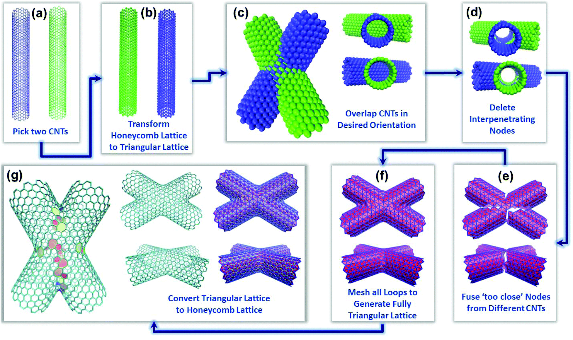 | ||
| Fig. 1 Schematic representation of various steps undertaken for the formation of CNT–CNT junction. | ||
Step (a): Pick two nanotubes of any desired chirality of desired length.
Step (b): Transform the honeycomb lattice of both nanotubes to triangular lattices (t-CNT) by calculating the centroid of each hexagon. Connect nearby nodes (1st co-ordination shell) to create a connected network.
Step (c): Put the two nanotubes (t-CNTs) in any desired spatial orientation, where they either fully or partially overlap with each other (certain degree of overlap is necessary for successful CNT junction formation).
Step (d): Delete all the interpenetrating nodes of the t-CNTs. Here, node deletion is performed by checking the radial distance of each t-CNT node from the axis of the other t-CNT. If the radial distance is less than the radius of the other t-CNT, the node is deleted. This operation is performed with respect to both t-CNT nodes. This operation also results in a set of surface nodes and surface edges (edges, which are a part of only one triangle).
Step (e): t-CNTs are then analyzed for node pairs with close spatial proximity (one node each from both t-CNTs within the spatial distance of 1 Å). If such a pair is found, it is fused into a single node. The spatial coordinates of the fused node are then updated to be the average of the coordinates of the original “too close” node pair. This is done for all such pairs found. Once all such nodes are fused, they create open loops across the junction (see Fig. 1e).
Step (f): Next step is to close (or stitch) each open loop. This is done by connecting surface nodes from different CNTs to create a fully triangular mesh of the fused junction. There are several possibilities with regard to how the loops are arranged in space, which require slightly different approaches to stitch them around the junction. For space considerations, the details of how the stitching is performed are discussed in ESI S3†via several examples. The ESI† also discusses the stitching of completely open loops (neighboring loops where no pairs exist within the spatial proximity of 1 Å).
Step (g): Once a fully triangular mesh is generated after stitching, this mesh is transformed to a honeycomb mesh (its dual) via calculating the centroid of each triangular element, which essentially results in a completely fused CNT junction (see Fig. 1g).
In Fig. 1g, all the non-hexagonal rings are colored for the sake of defect visualization. On close inspection, it is observed that this representative junction has 19 heptagons, 9 pentagons, 2 octagons, and 1 4-membered ring. The calculation of bond surplus with such defect topology leads to bond surplus value of +12 (calculated as (19 × 1) + (9 × −1) + (2 × 2) − (1 × −2)), which is in complete agreement with eqn (2).
Extension of framework to incorporate nanotubes' degrees of freedom
It is to be noted that the junction formulated above is not a unique junction (in terms of number and placement of non-hexagonal rings) for a given set of initial nanotube specifications (chirality, relative orientation, and degree of overlap). For example, a small or minute translation or rotation of either t-CNT along its respective axis will result in a significantly different triangular mesh topology of the fused junction, which in turn will lead to a topologically different arrangement of the defects in the resulting honeycomb junction. A demonstration of such an effect is shown in Fig. 2, which raises the following question. How does one account for such degrees of freedom (DOFs) towards determining the most stable junction structure under the given set of initial nanotube specifications?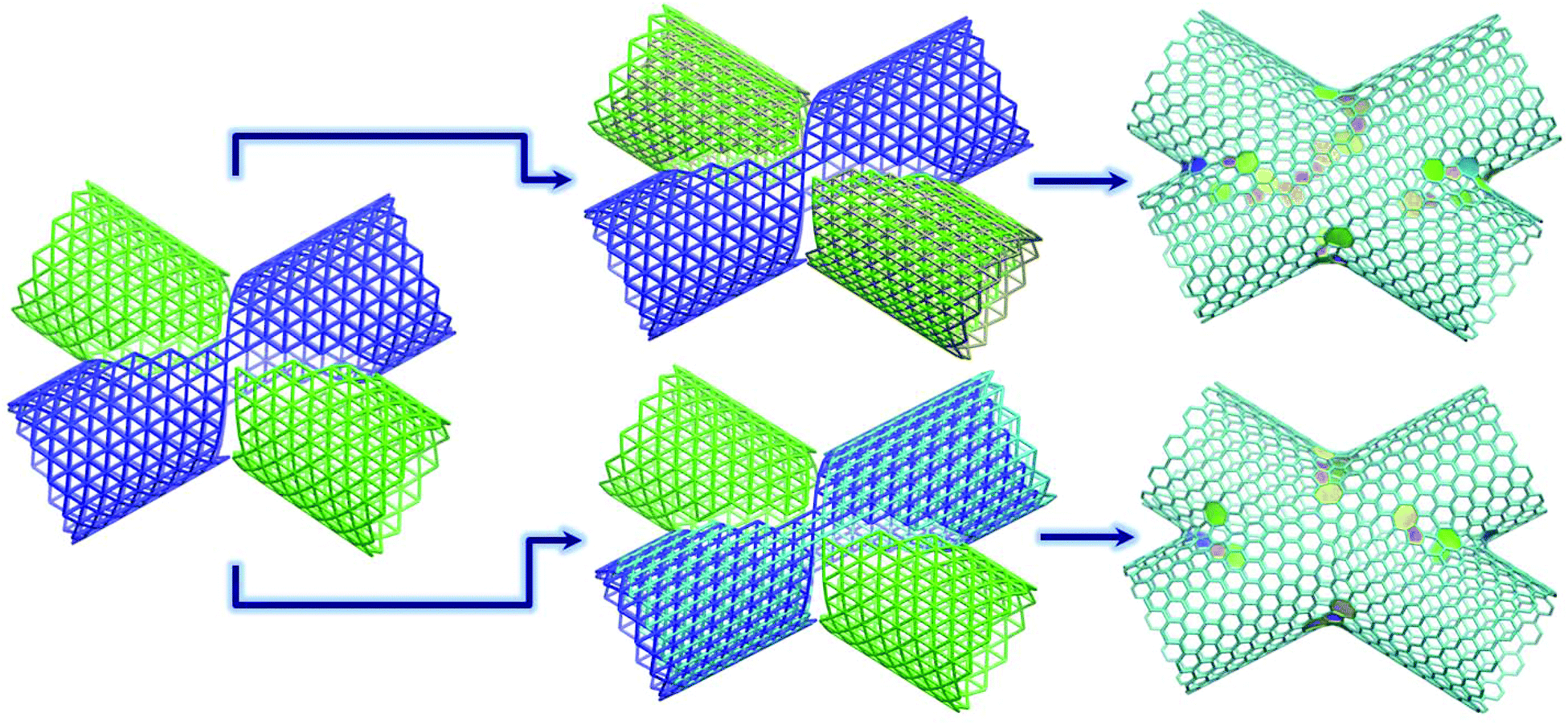 | ||
| Fig. 2 Effect of minute translation and rotation of t-CNTs on final defect topology of the created junction (right of the figure; non-hexagonal rings are shown as filled polygons in different colors). Top: Green t-CNT is translated and rotated along its axis (seen in brown color). Bottom: Blue t-CNT is translated and rotated along its axis (seen in cyan color). | ||
In total, there are 4 DOFs for a single CNT–CNT junction arising from the rotation and translation of each nanotube along its respective axis. Next, we discuss how a generic nanotube is translated and rotated to a desired degree along its cylindrical axis to account for the 4 DOFs mentioned above. Fig. 3a shows a segment of (9,3) t-CNT, where a triangular lattice unit cell is displayed in a bold red color. Fig. 3b shows the same lattice with respect to its lattice vectors,  and
and  , the nanotubes' cylindrical axis vector
  , and nanotube circumferential vector,
  , from a certain node (labeled as N). We choose (9,3) t-CNT for generalizing the discussion as neither of the lattice vectors (
 and
and  ) coincide with either cylindrical vector (
 or
or  ).
).
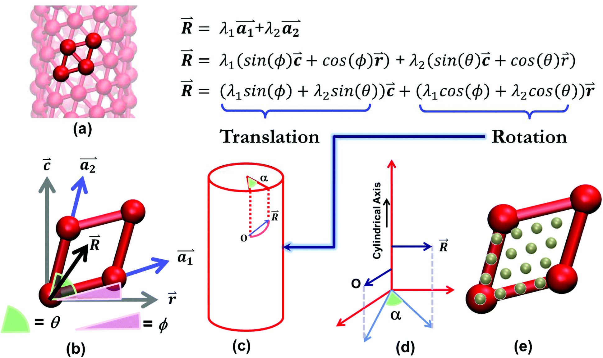 | ||
| Fig. 3 Schematic representation showcasing the key process features with regard to translational and rotational degrees of freedom towards the formation of the CNT junction. Various sub-figures (a–d) are discussed in detail in the main text. | ||
The premise of our approach is to rotate and translate the t-CNT such that node N can be shifted to any position within the lattice unit cell (along the circumference), given that the positioning of the cylindrical axis of the t-CNT remains the same. By doing so, it is possible, in principle, to scan through all likely combinations of CNT configurations for the junction formation. The following discussion shows how the shifting of node N by a vector  within the unit cell (along circumferential surface of the t-CNT; Fig. 3b) can be decoupled into simple t-CNT translation and rotation operations.
For this discussion, we translate our frame of reference so that node N resides at the origin, vector  is along the CNT axis, and vector
  is a circumferential tangent perpendicular to vector
  . In this reference, lattice vectors
  and
and  can be written in terms of vectors
  and
and  as follows.
 | (3.1) |
 | (3.2) |
 and
and  with vector
  . In the same frame of reference, any vector
  within the lattice unit can be written in terms of
  and
and  (see Fig. 3b), where λ1 and λ2 are both <1. On substituting
  and
and  in equation for
  , vector
  can be written in terms of
  and
and  decoupling the translational and rotational movement of t-CNT for translating node N by vector
  (see Fig. 3).
Here, the first term is the translation term along the  axis and is straightforward to implement. In the second term, the coefficient of vector
  is the distance along the circumferential perimeter that the node N needs to be rotated. Such a movement is implemented via rotation of the nanotube by angle α, which is depicted in Fig. 3c and is calculated from the dot product of two radial vectors, as shown in Fig. 3d. The two said vectors for the dot product are essentially the projections of two radial vectors (O and R; O representing radial origin vector of the unit cell while R representing radial vector of node N (depicted by vector
  ) originating from the CNT axis) on a plane perpendicular to the CNT axis. Fig. 3e shows a resulting movement of node N within the lattice, when the lattice is refined into 4 sub-divisions along vectors
  and
and  , resulting in 16 such nanotube configurations, based on value of λ1
 and λ2
 .
.
Next, we illustrate this approach for the (12,12) SWCNT–SWCNT junction fused at an angle of 60° by creating a number of junctions with varying junction topology. For this example, we subdivide our lattice space into 4 sub-units (2 × 2 along  and
and  directions) for each t-CNT, resulting in the formulation of 16 possible junction structures. We identify these cases using the nomenclature NipqNjrs, where Ni and Nj represent the two nanotubes, p & q represent the lattice node movement along
  and
and  directions for Ni t-CNT, while r & s represent the same movement for Nj t-CNT, respectively. The topological signatures around the junction for these 16 formulated cases (in terms of number and type of defects) are shown in Table 2 (DABS and DRSQ represented in Table 2 will be detailed in the next sub-section). It can clearly be seen that minor independent rotation and translation of each nanotube (for same degree of overlap and spatial orientation) results in significant differences in the number and topological signature of defects. The topological arrangement of defects in these 16 cases is visually shown in Fig. 4. We should point out that for each formulated junction, the bond surplus value is indeed +12, confirming Euler's polyhedral formula. It should be noted that, in principle, it is also possible to refine and perform this procedure via finer subdivision of the lattice (3 or more subdivisions along each vector). Such lattice refinement using n subdivisions will lead to n4 possible junction structures. It is possible that such fine subdivisions may lead to many junctions with the same topological signature around the junction (degenerate structures).
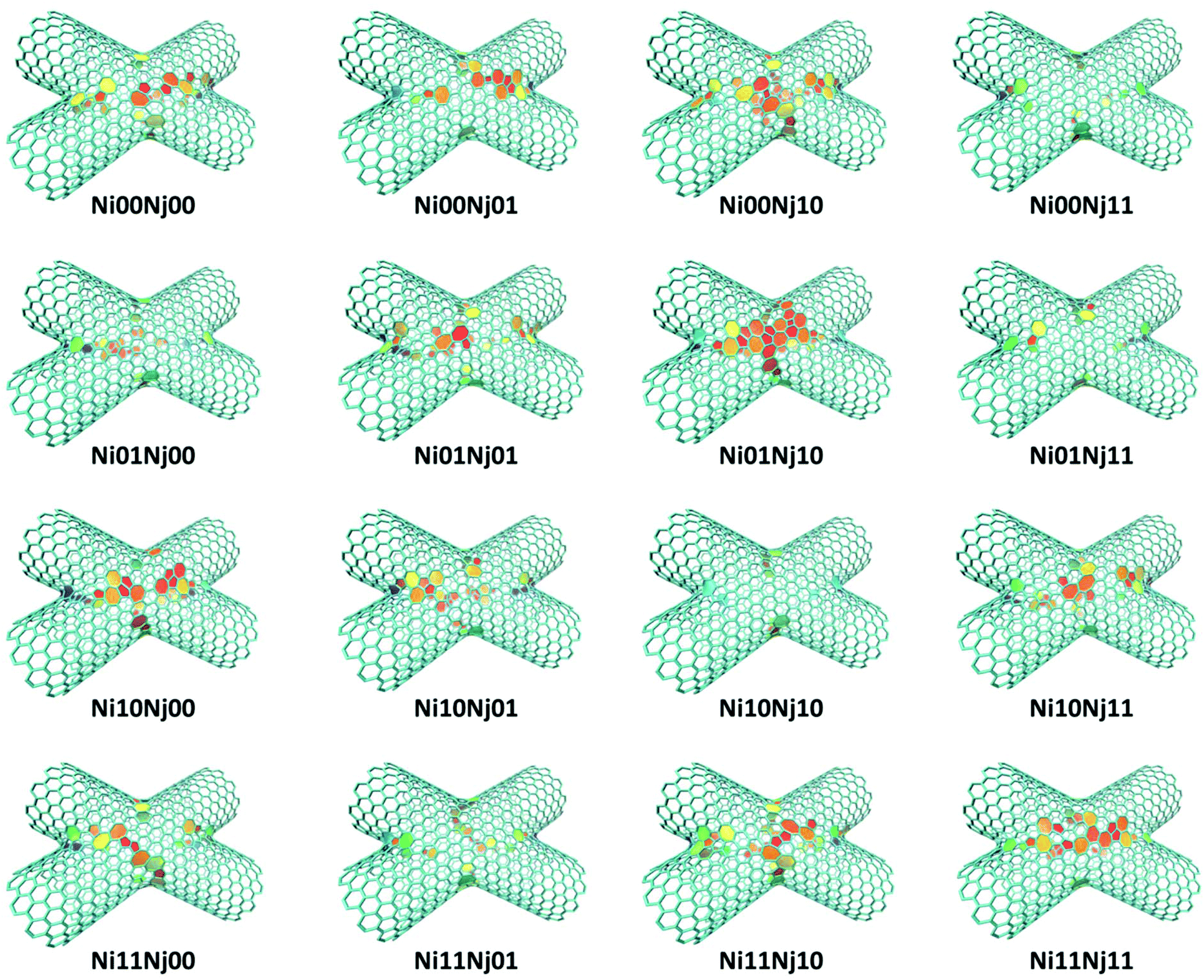 | ||
| Fig. 4 Topological arrangements of defects (non-hexagonal rings) in the studied 16 representative cases, considering the translation and rotation of both nanotubes. The defects are shown as colored polygons, where the color is representative of the area under the polygon which qualitatively increases as color changes: red → orange → green → blue. | ||
| Case # | 4Ma | 5Ma | 7Ma | 8Ma | D RSQ | D ABS | Total energy (kcal/mol) | Number of atoms | Energy/atom (kcal mol−1) |
|---|---|---|---|---|---|---|---|---|---|
| a Here, 4M, 5M, 7M, and 8M correspond to 4-membered rings, 5-membered rings (pentagons), 7-membered rings (heptagons), and 8-membered rings (octagons), respectively. | |||||||||
| Ni00Nj00 | 0 | 14 | 24 | 1 | 6.48 | 40 | 62![[thin space (1/6-em)]](https://www.rsc.org/images/entities/char_2009.gif) 838.2 838.2 |
1350 | 46.5468 |
| Ni00Nj01 | 1 | 9 | 19 | 2 | 6.32 | 34 | 62268.1 |
1344 | 46.3304 |
| Ni00Nj10 | 2 | 17 | 33 | 0 | 7.62 | 54 | 63443.7 |
1356 | 46.7874 |
| Ni00Nj11 | 0 | 8 | 20 | 0 | 5.29 | 28 | 62499.6 |
1352 | 46.2275 |
| Ni01Nj00 | 1 | 9 | 19 | 2 | 6.32 | 34 | 62320.9 |
1344 | 46.3697 |
| Ni01Nj01 | 0 | 14 | 24 | 1 | 6.48 | 40 | 62875.5 |
1350 | 46.5744 |
| Ni01Nj10 | 2 | 17 | 33 | 0 | 7.62 | 54 | 63473.0 |
1356 | 46.809 |
| Ni01Nj11 | 0 | 8 | 20 | 0 | 5.29 | 28 | 62510.6 |
1352 | 46.2356 |
| Ni10Nj00 | 0 | 13 | 23 | 1 | 6.32 | 38 | 63220.2 |
1362 | 46.4172 |
| Ni10Nj01 | 0 | 13 | 23 | 1 | 6.32 | 38 | 63203.6 |
1362 | 46.405 |
| Ni10Nj10 | 0 | 4 | 12 | 2 | 4.90 | 20 | 61886.8 |
1344 | 46.0468 |
| Ni10Nj11 | 0 | 12 | 20 | 2 | 6.32 | 36 | 63398.5 |
1364 | 46.4798 |
| Ni11Nj00 | 0 | 13 | 25 | 0 | 6.16 | 38 | 62423.0 |
1346 | 46.3767 |
| Ni11Nj01 | 0 | 13 | 25 | 0 | 6.16 | 38 | 62414.0 |
1346 | 46.37 |
| Ni11Nj10 | 0 | 16 | 28 | 0 | 6.63 | 44 | 62740.2 |
1348 | 46.5432 |
| Ni11Nj11 | 0 | 14 | 26 | 0 | 6.32 | 40 | 62404.0 |
1344 | 46.4315 |
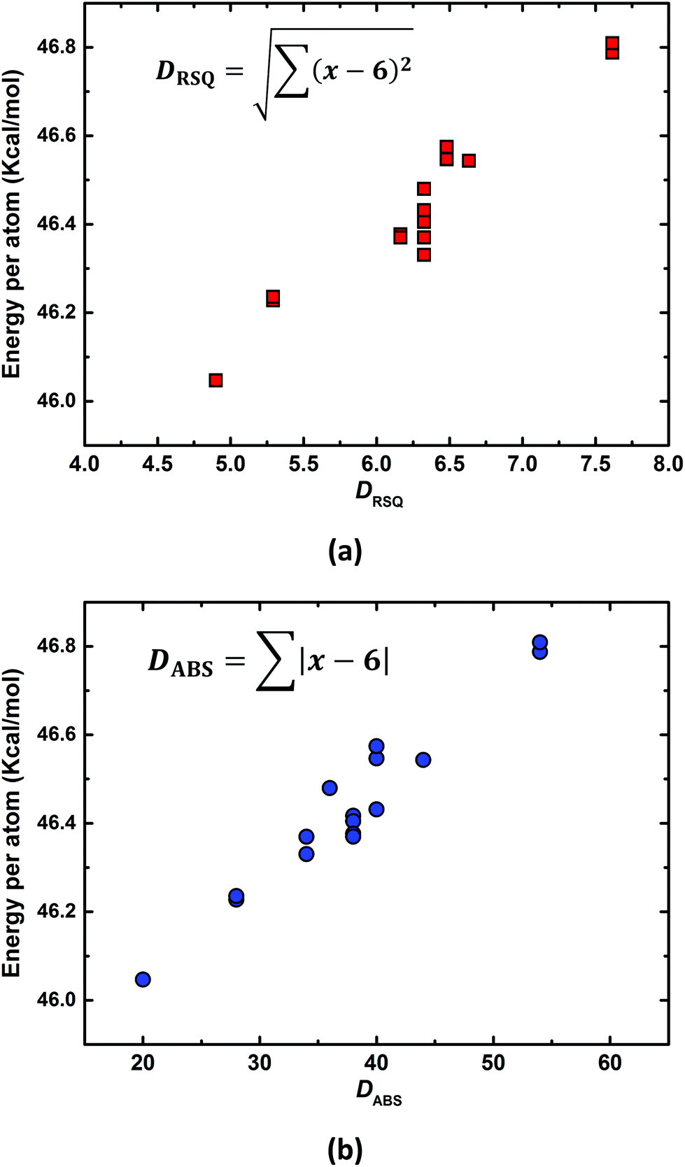
Correlation between relative stability of junctions and degree of topological defects
Next, we minimize each of the 16 generated cases via the molecular mechanics method using LAMMPS software,60 where PCFF force field61 is used to define bonded and non-bonded interactions to predict their relative stability. In principle, such a minimization can be performed using any carbon-based force field (see ESI S4† for comparison of different force fields with respect to the energies of the minimized 16 cases). Table 2 also depicts the energy/atom of the minimized structure. It is to be noted that the energy prediction for relative stability is obtained in terms of energy/atom instead of total energy of the nanostructured junction as the final number of atoms in various formulated junctions are somewhat different (between 1344 and 1364; please refer to Table 2). In principle, one could identify many other such energy-related criteria, such as bond energy/atom, angle energy/atom, dihedral energy/atom, per atom residual stress, and distribution of differences in bond lengths, angles, and dihedral angles from their equilibrium values, to characterize junction stability. The primary reason for using “energy/atom” for our study is the observation that “energy/atom” reflects the combination of all multi-dimensional variables into a one-dimensional measure.From Table 2, it can clearly be seen that depending upon the topological arrangement of the junctions, there exist notable differences between the energy/atom and relative stability for different formulated junctions. In order to estimate the possible correlation between the relative stability of the junctions with the number and topological arrangements of defects, we plotted the energy/atom of different test cases against two different defect characterization parameters, DRSQ and DABS, as shown in Fig. 5. The two defect parameters are calculated as follows. We first identify all the non-hexagonal rings around the junction. Then, we calculate the term (x − 6) for each such ring, where x corresponds to number of bonds in the ring. Thus, a pentagonal ring will lead to value of −1, while a heptagonal ring will lead to value of +1 (similar to the bond surplus discussion given previously). For DABS, we take the summation of absolute values (thus ABS) of all such terms, while DRSQ is the square root of summation of the squares of all such terms. The equations for the two defect parameters are highlighted within the graphs for further clarity.
 | ||
| Fig. 5 Plot showing energy/atom as a function of defect parameters (a) DRSQ and (b) DABS for the representative system discussed in the main text. RSQ and ABS refer to “root square” and “absolute” values, respectively. A decreasing trend in energy with decreasing DRSQ and DABS represents the correlation between degree of junction defects (non-hexagonal rings) and stability of the structure in terms of energy/atom. | ||
In general, it is noted that the larger the value of defect parameters, the higher the energy/atom of the minimized structures. Additionally, it is observed that for a similar number of defects (and thus their defect parameter values), their topological arrangement in space is also important with respect to their relative stability. For the same number of non-hexagonal defects (for example, see cases #Ni00Nj10 and #Ni01Nj10 in Fig. 4), if the defects are found to be adjacent, it is found to decrease the energy/atom, leading to a less stable structure. When the defects form a cluster (several non-hexagonal rings forming a cluster), it is expected to increase local atomic stress (due to greater deviation from the ideal sp2 hybridized state), leading to lower stability of the structure. We should also mention that while a better measure for correlating topological arrangement of defects with relative junction stability can be deduced in principle, the currently analysis is presented to only highlight that the number, type, as well as the topological arrangement of the defects, all are important from the perspective of junction stability.
Annihilation of topological defects
While we show that it is possible to create a variety of junction topologies by employing translational and rotational DOFs of t-CNTs, the story does not end here with respect to the quest for the identification of the most energetically stable junction. It is seen from various formulated cases (see visual representation in Fig. 1g and Fig. 4) that, more often than not, the non-hexagonal rings (i.e., defect sites) are either adjacent to each other or they form a mini-cluster. We show that it is possible to either annihilate such defect clusters or reduce them to a single defect via manipulation of the underlying triangular mesh,62 resulting in more stable honeycomb-meshed CNT junctions.The triangular mesh can be manipulated using four different operations, namely, vertex delete (VD), vertex split (VS), edge flip (EF), and edge collapse (EC).62 The schematics of these 4 operations are highlighted in Fig. 6. In t-CNT junctions (see Fig. 1f), these operations can be used to reduce and annihilate the defects, which in turn results in a more stable nanotube junction. Below, we discuss 6 different types of defect clusters that may be present in a formulated junction that can either be annihilated or reduced to a single defect using one of the 4 aforementioned operations. The graphical representation of defect reduction processes for these 6 different defect clusters and the resulting local structure of the nanostructure are shown in Fig. 7.
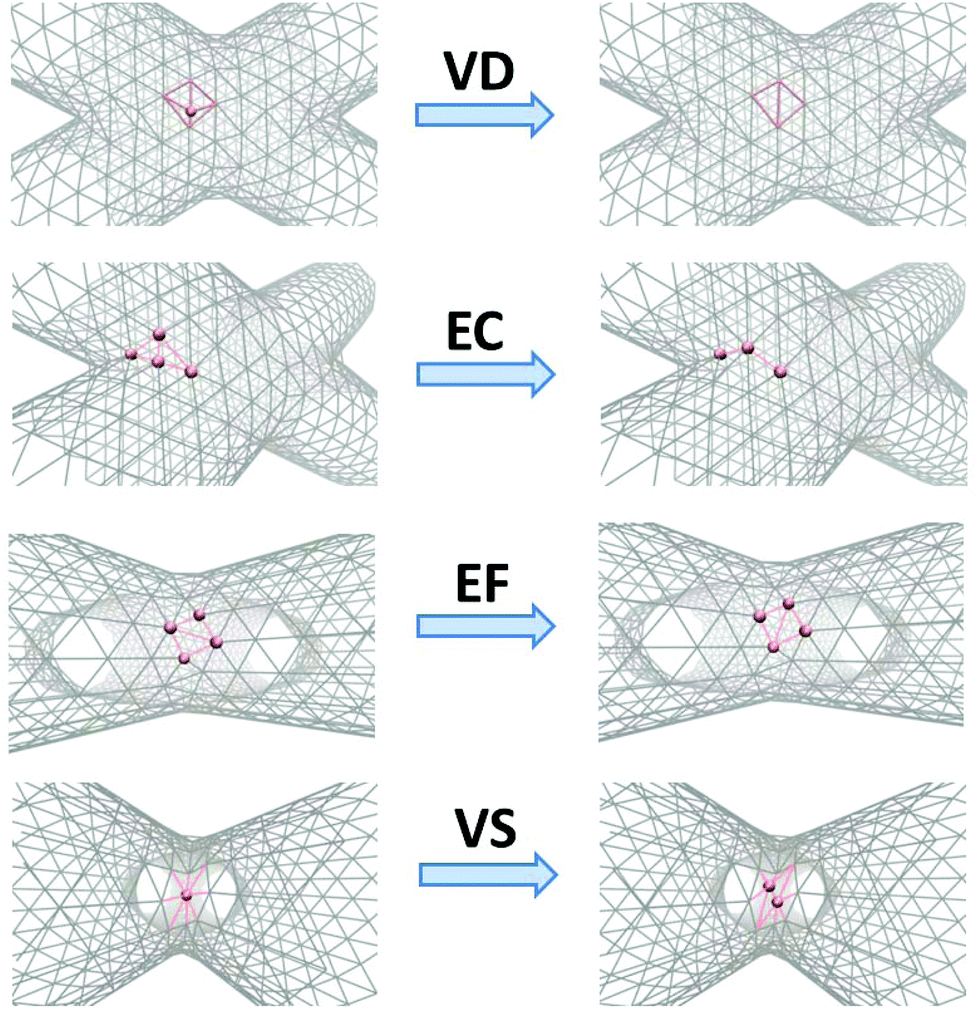 | ||
| Fig. 6 Schematic representation of 4 different node manipulation operations as discussed in the text. VD, EC, EF, and VS refer to vertex delete, edge collapse, edge flip, and vertex split operations, respectively. | ||
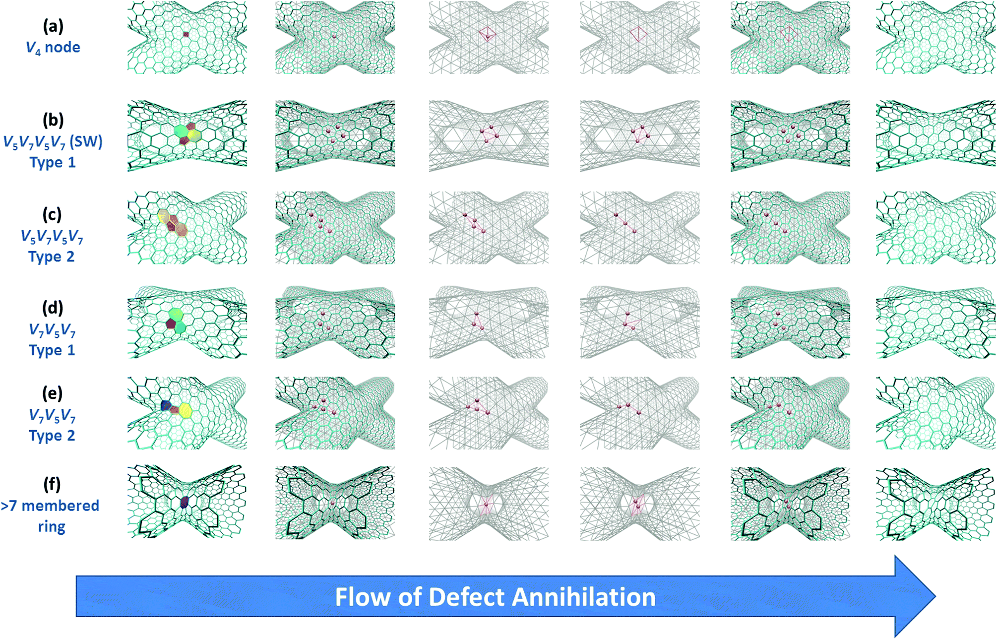 | ||
| Fig. 7 Schematic representation showing annihilation/reduction of 6 different types of defects via node and edge manipulation. | ||
It can be seen that among these operations, all but EF operation lead to a different number of carbon atoms in the final resulting structure. VD and EC delete 2 triangles, lowering the carbon atom count by 2, while VS adds 2 triangles, increasing the carbon count by 2 in the resulting honeycomb meshes. EF node mesh manipulation does not change any triangle count within the triangular mesh, thus leading to the same number of carbon atoms in the resulting honeycomb mesh. It should also be noted that these operations do not alter the bond surplus count at all; this value still remains +12 for a single CNT–CNT junction. In addition to annihilation of the defects, it is possible to move defects (such as v5 − v7 defect pair) from one location to another around the junction. Such examples of defect movement via EF, EC and VS operations have been discussed in detail by Li et al.62
We performed these set of operations on each of the 16 developed cases to analyze the energy/atom trends with reduction in defects. A representative process of defect reduction and energy decrease is shown in Table 3 for 3 of the 16 cases, showing the correlation between defect reduction and relative junction stability (in terms of energy/atom). In addition, Fig. 8 shows the graphical representation of the correlation between defect reduction (in terms of defect parameter DABS) and the lowering of resulting energy/atom for each of the 16 cases as defects are reduced/annihilated in each of them. A similar representation in terms of defect parameter DRSQ is also shown in ESI S5† for interested readers. Based on this analysis, we can argue that the discussed 4 operations can be effectively used to relax “raw” junctions (which are formulated via geometric considerations only) substantially to relatively more stable configurations.
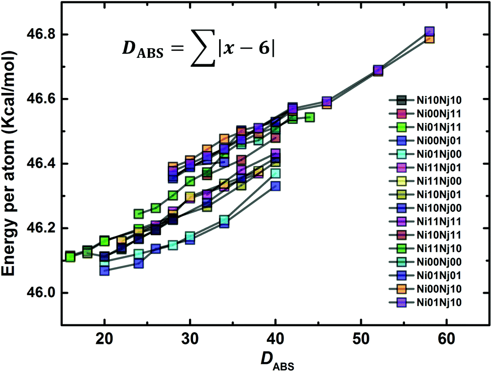 | ||
| Fig. 8 Plot showing energy/atom as a function of defect parameter DABS for 16 different created systems (shown in different colors). The decrease in energy for each color with decreasing DABS represents the correlation between degree of junction defects (non-hexagonal rings) and stability of the structure in terms of energy/atom. | ||
| Case # | 4M | 5M | 7M | 8M | D RSQ | D ABS | Energy/Atom (kcal mol−1) | Operation |
|---|---|---|---|---|---|---|---|---|
| Ni10Nj10.honeycomb.lammps | 0 | 4 | 12 | 2 | 4.90 | 20 | 46.0467 | EC (V7V5V7) |
| Ni10Nj10.honeycomb.lammps.min.0 | 0 | 3 | 11 | 2 | 4.69 | 18 | 46.0148 | EC (V7V5V7) |
| Ni10Nj10.honeycomb.lammps.min.1 | 0 | 2 | 10 | 2 | 4.47 | 16 | 45.9926 | EC (V7V5V7) |
| Ni10Nj10.honeycomb.lammps.min.2 | 0 | 1 | 9 | 2 | 4.24 | 14 | 45.9664 | EC (V7V5V7) |
| Ni10Nj10.honeycomb.lammps.min.3 | 0 | 0 | 8 | 2 | 4.00 | 12 | 45.9387 | |
| Ni00Nj11.honeycomb.lammps | 0 | 8 | 20 | 0 | 5.29 | 28 | 46.2275 | EC (V7V5V5V7) |
| Ni00Nj11.honeycomb.lammps.min.0 | 0 | 6 | 18 | 0 | 4.90 | 24 | 46.1926 | EF (V7V5V5V7) |
| Ni00Nj11.honeycomb.lammps.min.1 | 0 | 4 | 16 | 0 | 4.47 | 20 | 46.1622 | EF (V7V5V7) |
| Ni00Nj11.honeycomb.lammps.min.2 | 0 | 3 | 15 | 0 | 4.24 | 18 | 46.1316 | EF (V7V5V7) |
| Ni00Nj11.honeycomb.lammps.min.3 | 0 | 2 | 14 | 0 | 4.00 | 16 | 46.1152 | |
| Ni01Nj11.honeycomb.lammps | 0 | 8 | 20 | 0 | 5.29 | 28 | 46.2357 | EF (V7V5V5V7) |
| Ni01Nj11.honeycomb.lammps.min.0 | 0 | 6 | 18 | 0 | 4.90 | 24 | 46.1974 | EC (V7V5V5V7) |
| Ni01Nj11.honeycomb.lammps.min.1 | 0 | 4 | 16 | 0 | 4.47 | 20 | 46.1596 | EC (V7V5V7) |
| Ni01Nj11.honeycomb.lammps.min.2 | 0 | 3 | 15 | 0 | 4.24 | 18 | 46.1284 | EF (V7V5V7) |
| Ni01Nj11.honeycomb.lammps.min.3 | 0 | 2 | 14 | 0 | 4.00 | 16 | 46.1107 | |
In summary, our idea revolves around the quest to obtain the most stable junction structure under the given set of nanotube conditions. However, it can be seen that various junction configurations can be generated during this process, which have different degrees of relative stability. Identification of such junctions can be useful in investigating the effect of differences in local arrangement of topological defects around the junction on various junction associated properties such as electronic transmission across the junction, phonon propagation or scattering at the junction, and mechanical properties (such as failure strength of the junction). It is expected that such properties will depend on local topological arrangement of non-hexagonal rings around the junction. For example, Romo-Herrera et al. have shown that the nature of non-hexagonal rings around the junction does affect the electronic and mechanical properties of the nanotube junctions.37,38,40 Another study performed by Yang et al. has also shown that failure characteristics of CNT-graphene hybrid nanostructures are strongly dependent on the topological arrangement of non-hexagonal defects around the CNT-graphene junction, with higher strength observed for junctions where defects (non-hexagonal rings) are separated by hexagonal rings.63
Extension to other carbon nanostructures
Similar to CNTs, other types of carbon nanostructures such as fullerenes, graphene, and nanocones also consist of sp2 hybridized carbon atoms and possess a similar honeycomb lattice structure. It is thus imperative that the discussed framework can be extended to fuse such nanostructures as well and create junctions and grain boundaries between similar or different types of carbon nanostructures. In Fig. 9, we have shown few examples of junctions that are created via our framework between similar and different types of carbon nanostructures.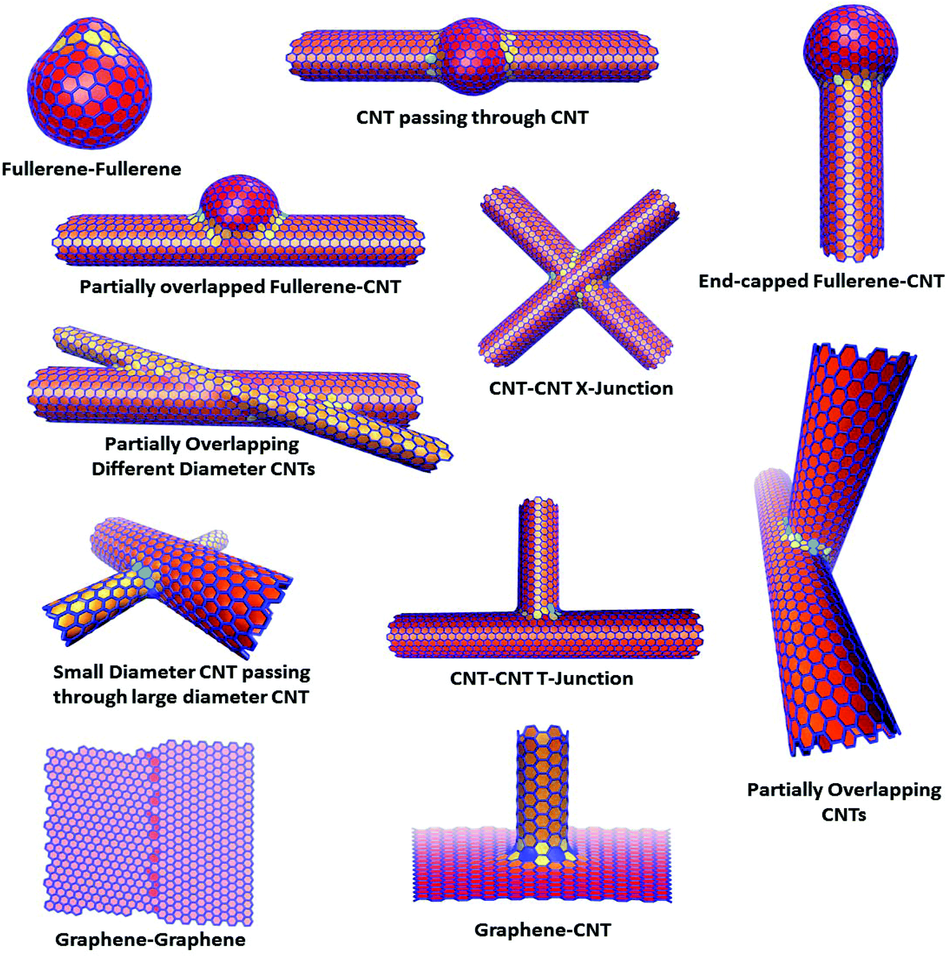 | ||
| Fig. 9 Representation of different types of junctions and grain boundaries as developed by the discussed framework between similar and different types of carbon nanostructures. | ||
Conclusions and outlook
In this work, we have outlined a generic framework for creating junctions between two nanotubes with arbitrary intrinsic features (chirality) and their relative spatial positioning (angular orientation and degree of partial overlap). We also provide a systematic approach to annihilate various types of defects and customize the topological arrangement around the junction towards achieving the most stable junction for a given set of CNTs and their relative spatial positioning. The procedure works with triangular meshes and makes use of the primal/dual meshing concept to render a fused junction with honeycomb mesh elements. This framework can easily be extended to create multi-wall nanotube junctions, multi-nanotube clusters, and large-scale random nanotube networks. Fig. 10 shows typical schematics of a multi-wall CNT junction and a multi-nanotube cluster, as created by the outlined framework.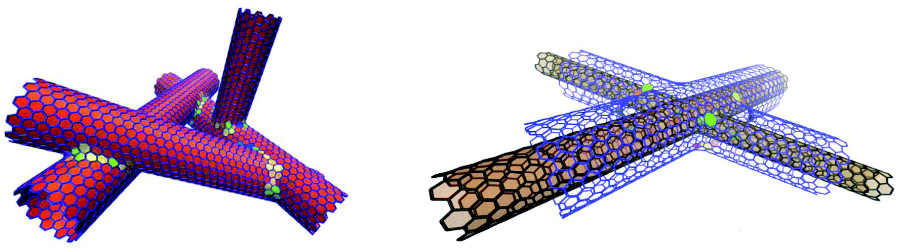 | ||
| Fig. 10 Representative example showcasing (a) a multi-nanotube cluster and (b) a multi-wall CNT junction, where the inner-junction is between (5,5) and (7,7) CNTs, while the outer-junction is between (10,10) and (12,12) CNTs. In (b), the outer-CNT junction is shown as a transparent structure where only non-hexagonal defect sites are highlighted for clarity. | ||
It should also be pointed out that as the discussed framework makes excellent use of triangular/honeycomb primal/dual concept, it also opens up opportunities to create and investigate junctions and grain boundaries for other kinds of material interfaces that exhibit the honeycomb lattice as their unit cell, such as h-BN, transition-metal dichalcogenides (TMDs) and wurtzite lattice structures (GaN, ZnO).
Conflicts of interest
The authors declare no conflicts of interest.Acknowledgements
VV would like to acknowledge AFOSR (Lab Task: 15RXCOR140 (PM: Dr. Joycelyn Harrison)) for financial support. VU would like to acknowledge the support of the NASA Alabama EPSCoR 2015 RID seed grants and the US Air Force Summer Faculty Fellowships with Dr. Ajit Roy.References
- D. Zhou and S. Seraphin, Chem. Phys. Lett., 1995, 238, 286–289 CrossRef.
- F. L. Deepak, A. Govindaraj and C. N. R. Rao, Chem. Phys. Lett., 2001, 345, 5–10 CrossRef CAS.
- W. Z. Li, J. G. Wen and Z. F. Ren, Appl. Phys. Lett., 2001, 79, 1879–1881 CrossRef CAS.
- A. V. Krasheninnikov and F. Banhart, Nat. Mater., 2007, 6, 723–733 CrossRef CAS PubMed.
- M. Terrones, F. Banhart, N. Grobert, J. C. Charlier, H. Terrones and P. Ajayan, Phys. Rev. Lett., 2002, 89, 075505 CrossRef CAS PubMed.
- F. Banhart, Nano Lett., 2001, 1, 329–332 CrossRef CAS.
- J.-M. Ting and C.-C. Chang, Appl. Phys. Lett., 2002, 80, 324–325 CrossRef CAS.
- Y. C. Choi and W. Choi, Carbon, 2005, 43, 2737–2741 CrossRef CAS.
- S. Tawfick, K. O'Brien and A. J. Hart, Small, 2009, 5, 2467–2473 CrossRef CAS PubMed.
- M. A. Worsley, S. O. Kucheyev, J. H. Satcher, A. V. Hamza and T. F. Baumann, Appl. Phys. Lett., 2009, 94, 073115 CrossRef.
- P. W. Chiu, G. S. Duesberg, U. Dettlaff-Weglikowska and S. Roth, Appl. Phys. Lett., 2002, 80, 3811–3813 CrossRef CAS.
- P. W. Chiu, M. Kaempgen and S. Roth, Phys. Rev. Lett., 2004, 92, 246802 CrossRef PubMed.
- H. W. C. Postma, M. de Jonge, Z. Yao and C. Dekker, Phys. Rev. B: Condens. Matter Mater. Phys., 2000, 62, R10653–R10656 CrossRef CAS.
- Y. Fu, B. Carlberg, N. Lindahl, N. Lindvall, J. Bielecki, A. Matic, Y. Song, Z. Hu, Z. Lai, L. Ye, J. Sun, Y. Zhang, Y. Zhang and J. Liu, Adv. Mater., 2012, 24, 1576–1581 CrossRef CAS PubMed.
- F. Du, D. Yu, L. Dai, S. Ganguli, V. Varshney and A. K. Roy, Chem. Mater., 2011, 23, 4810–4816 CrossRef CAS.
- Z. Yan, L. Ma, Y. Zhu, I. Lahiri, M. G. Hahm, Z. Liu, S. Yang, C. Xiang, W. Lu, Z. Peng, Z. Sun, C. Kittrell, J. Lou, W. Choi, P. M. Ajayan and J. M. Tour, ACS Nano, 2013, 7, 58–64 CrossRef CAS PubMed.
- S. H. Lee, D. H. Lee, W. J. Lee and S. O. Kim, Adv. Funct. Mater., 2011, 21, 1338–1354 CrossRef CAS.
- D. Wei and Y. Liu, Adv. Mater., 2008, 20, 2815–2841 CrossRef CAS.
- L. Sun, M. Li, Y. Jiang, W. Kong, K. Jiang, J. Wang and S. Fan, Nano Lett., 2014, 14, 4044–4049 CrossRef CAS PubMed.
- W. Wang, S. Guo, M. Penchev, I. Ruiz, K. N. Bozhilov, D. Yan, M. Ozkan and C. S. Ozkan, Nano Energy, 2013, 2, 294–303 CrossRef CAS.
- M. Kaempgen, J. Ma, G. Gruner, G. Wee and S. G. Mhaisalkar, Appl. Phys. Lett., 2007, 90, 264104 CrossRef.
- H. Chen, M. Chen, J. Di, G. Xu, H. Li and Q. Li, J. Phys. Chem. C, 2012, 116, 3903–3909 CAS.
- D. J. Cohen, D. Mitra, K. Peterson and M. M. Maharbiz, Nano Lett., 2012, 12, 1821–1825 CrossRef CAS PubMed.
- K. H. Kim, Y. Oh and M. F. Islam, Nat. Nanotechnol., 2012, 7, 562–566 CrossRef CAS PubMed.
- D. P. Hashim, N. T. Narayanan, J. M. Romo-Herrera, D. A. Cullen, M. G. Hahm, P. Lezzi, J. R. Suttle, D. Kelkhoff, E. Munoz-Sandoval, S. Ganguli, A. K. Roy, D. J. Smith, R. Vajtai, B. G. Sumpter, V. Meunier, H. Terrones, M. Terrones and P. M. Ajayan, Sci. Rep., 2012, 2, 363 CrossRef PubMed.
- C. Wang, K. Takei, T. Takahashi and A. Javey, Chem. Soc. Rev., 2013, 42, 2592–2609 RSC.
- D. Estrada and E. Pop, Appl. Phys. Lett., 2011, 98, 073102 CrossRef.
- H. Z. Geng, K. K. Kim, K. P. So, Y. S. Lee, Y. Chang and Y. H. Lee, J. Am. Chem. Soc., 2007, 129, 7758–7759 CrossRef CAS PubMed.
- S. H. Ke, H. U. Baranger and W. Yang, Phys. Rev. Lett., 2007, 99, 146802 CrossRef PubMed.
- J. W. Do, D. Estrada, X. Xie, N. N. Chang, J. Mallek, G. S. Girolami, J. A. Rogers, E. Pop and J. W. Lyding, Nano Lett., 2013, 13, 5844–5850 CrossRef CAS PubMed.
- K. H. Khoo and J. R. Chelikowsky, Phys. Rev. B: Condens. Matter Mater. Phys., 2009, 79, 205422 CrossRef.
- R. A. Bell, M. C. Payne and A. A. Mostofi, Phys. Rev. B: Condens. Matter Mater. Phys., 2014, 89, 245426 CrossRef.
- C. Dekker, Z. Yao, H. W. C. Postma and L. Balents, Nature, 1999, 402, 273–276 CrossRef.
- L. Chico, V. H. Crespi, L. X. Benedict, S. G. Louie and M. L. Cohen, Phys. Rev. Lett., 1996, 76, 971–974 CrossRef CAS PubMed.
- L. Chernozatonskii, J. Nanopart. Res., 2003, 5, 473–484 CrossRef CAS.
- V. Varshney, A. K. Roy, G. Froudakis and B. L. Farmer, Nanoscale, 2011, 3, 3679–3684 RSC.
- J. M. Romo-Herrera, M. Terrones, H. Terrones, S. Dag and V. Meunier, Nano Lett., 2007, 7, 570–576 CrossRef CAS PubMed.
- J. M. Romo-Herrera, M. Terrones, H. Terrones and V. Meunier, ACS Nano, 2008, 2, 2585–2591 CrossRef CAS PubMed.
- R. Zhou, R. Liu, L. Li, X. Wu and X. C. Zeng, J. Phys. Chem. C, 2011, 115, 18174–18185 CAS.
- J. M. Romo-Herrera, M. Terrones, H. Terrones and V. Meunier, Nanotechnology, 2008, 19, 315704 CrossRef CAS PubMed.
- Y. Li, X. Qiu, Y. Yin, F. Yang and Q. Fan, J. Phys. D: Appl. Phys., 2009, 42, 155405 CrossRef.
- Y. Li, X. Qiu, F. Yang, X. S. Wang and Y. Yin, Nanotechnology, 2008, 19, 225701 CrossRef PubMed.
- T. Ketolainen, V. Havu and M. J. Puska, J. Chem. Phys., 2015, 142, 054705 CrossRef CAS PubMed.
- X. Yang, D. Chen, Z. Han, X. Ma and A. C. To, Int. J. Heat Mass Transfer, 2014, 70, 803–810 CrossRef CAS.
- S. Imani Yengejeh, M. Akbar Zadeh and A. Öchsner, Appl. Phys. A, 2013, 115, 1335–1344 CrossRef.
- S. Imani Yengejeh, M. Akbar Zadeh and A. Öchsner, Comput. Mater. Sci., 2014, 92, 76–83 CrossRef CAS.
- S. I. Yengejeh, S. A. Kazemi and A. Öchsner, J. Nano Res., 2017, 47, 120–127 CrossRef.
- I. Zsoldos, G. Kakuk, T. Réti and A. Szasz, Modell. Simul. Mater. Sci. Eng., 2004, 12, 1251–1266 CrossRef CAS.
- S. Melchor and J. A. Dobado, J. Chem. Inf. Comput. Sci., 2004, 44, 1639–1646 CrossRef CAS PubMed.
- S. Melchor, F. J. Martin-Martinez and J. A. Dobado, J. Chem. Inf. Model., 2011, 51, 1492–1505 CrossRef CAS PubMed.
- I. Jang, S. B. Sinnott, D. Danailov and P. Keblinski, Nano Lett., 2004, 4, 109–114 CrossRef CAS.
- N. M. Piper, Y. Fu, J. Tao, X. Yang and A. C. To, Chem. Phys. Lett., 2011, 502, 231–234 CrossRef CAS.
- I. Ponomareva, L. A. Chernozatonskii, A. N. Andriotis and M. Menon, New J. Phys., 2003, 5, 119 CrossRef.
- M. Menon, A. Andriotis, D. Srivastava, I. Ponomareva and L. Chernozatonskii, Phys. Rev. Lett., 2003, 91, 145501 CrossRef PubMed.
- T. Petersen, I. Snook, I. Yarovsky and D. McCulloch, Phys. Rev. B: Condens. Matter Mater. Phys., 2005, 72, 125417 CrossRef.
- E. Biyikli, J. Liu, X. Yang and A. C. To, RSC Adv., 2013, 3, 1359–1362 RSC.
- H. Terrones and A. L. Mackay, Carbon, 1992, 30, 1251–1260 CrossRef CAS.
- V. Varshney, S. S. Patnaik, A. K. Roy, G. Froudakis and B. L. Farmer, ACS Nano, 2010, 4, 1153–1161 CrossRef CAS PubMed.
- G. K. Dimitrakakis, E. Tylianakis and G. E. Froudakis, Nano Lett., 2008, 8, 3166–3170 CrossRef CAS PubMed.
- S. Plimpton, J. Comput. Phys., 1995, 117, 1–19 CrossRef CAS.
- H. Sun, S. J. Mumby, J. R. Maple and A. T. Hagler, J. Am. Chem. Soc., 1994, 116, 2978–2987 CrossRef CAS.
- Y. Li, E. Zhang, Y. Kobayashi and P. Wonka, ACM Trans. Graph., 2010, 29, 153 Search PubMed.
- Y. Yang, N. D. Kim, V. Varshney, S. Sihn, Y. Li, A. K. Roy, J. M. Tour and J. Lou, Nanoscale, 2017, 9, 2916–2924 RSC.
Footnote |
| † Electronic supplementary information (ESI) available. See DOI: 10.1039/c7nr06659g |
| This journal is © The Royal Society of Chemistry 2018 |