
A location- and sharpness-specific tactile electronic skin based on staircase-like nanowire patches†
Shu
Gong‡
 ab,
Yan
Wang‡
ab,
Lim Wei
Yap
ab,
Yunzhi
Ling
ab,
Yunmeng
Zhao
ab,
Dashen
Dong
ab,
Qianqian
Shi
ab,
Yiyi
Liu
ab,
Hemayet
Uddin
c and
Wenlong
Cheng
*abc
ab,
Yan
Wang‡
ab,
Lim Wei
Yap
ab,
Yunzhi
Ling
ab,
Yunmeng
Zhao
ab,
Dashen
Dong
ab,
Qianqian
Shi
ab,
Yiyi
Liu
ab,
Hemayet
Uddin
c and
Wenlong
Cheng
*abc
aDepartment of Chemical Engineering, Monash University, Clayton, Victoria 3800, Australia. E-mail: wenlong.cheng@monash.edu
bNew Horizon Research Centre, Monash University, Clayton, Victoria 3800, Australia
cThe Melbourne Centre for Nanofabrication, Clayton, Victoria 3800, Australia
First published on 1st August 2018
Abstract
Human skin can sense an external object in a location-specific manner, simultaneously recognizing whether it is sharp or blunt. Such tactile capability can be achieved in both natural and stretched states. It is impractical to mimic this tactile function of human skin by designing pixelated sensor arrays across our whole curvilinear human body. Here, we report a new tactile electronic skin sensor based on staircase-like vertically aligned gold nanowires (V-AuNWs). With a back-to-back linear or spiral assembly of two staircase structures into a single sensor, we are able to recognize pressure in a highly location-specific manner for both non-stretched and stretched states (up to 50% strain); with a concentric design on the fingertip, we can identify the sharpness of an external object. We believe that our strategy opens up a new route to highly specific second-skin-like tactile sensors for electronic skin (E-skin) applications.
Conceptual insightsWe report a new tactile electronic skin sensor based on staircase-like vertically aligned gold nanowires (V-AuNWs). With the back-to-back linear or spiral assembly of two antiparallel staircase structures into a single sensor, we are able to recognize pressure in a highly location-specific manner for both non-stretched and stretched states (up to 50% strain). With a concentric design on the fingertip, we can identify the sharpness of an external object in a similar way to human skin for the first time. Note that only location-specific pressure sensing under a non-stretched state has been demonstrated with existing unpixellated pressure sensors. Other important functions of human tactile sensing, such as the ability to discriminate sharp/blunt objects and location-specific sensing under stretched states, have not yet been achieved in the literature. We believe that our methodologies open up a new route to low-cost stretchable smart tactile sensors with potential facile integration and high location resolution into future wearable electronics, such as stretchable touch-on displays, soft robotics and prosthetic skins. The staircase structures and location-specific sensitivity could be extended to other novel nanomaterials and designs to form heterogeneous multifunctional optoelectronic devices, indicating broad application potentiality in next-generation skin-like electronics. |
Introduction
A unique advantage of the human skin sensory system is its specificity. As far as pressure is concerned, our skin can detect where an external force is applied, simultaneously identifying whether it is a sharp or a blunt object. This can be achieved in either a non-stretched or a stretched state. To mimic this skin function for next-generation soft robotic and prosthetic applications,1–4 a plausible approach may be to fabricate pixelated sensor arrays registered to matrix circuitry by monitoring pressure-induced electric,3,5–11 magnetic12,13 and optical14,15 signal changes. However, this will require numerous wiring interconnections to realise reasonably large-area pressure mapping, hence rendering it impractical to apply a pixelated design approach to cover the entire curvilinear surfaces of the human body.Here, we report a non-pixelated tactile sensor based on staircase-like vertically-aligned gold nanowires (V-AuNWs). Using an antiparallel linear assembly, the sensor can recognize where an external load is applied and its strength. Such a location-specific sensing capability can also be achieved in the stretched state (up to 50% strain). Furthermore, we show that a staircase-like design can be extended to other configurations, such as spiral and concentric patterns. When a concentric pattern with antiparallel staircase V-AuNWs is attached to a human finger, a sharp or blunt object can be discriminated in a similar way to human skin.
Our design principle is based on the accurate thickness control of V-AuNWs, which is key to staircase structural design. Previously, carbon nanotubes,6,7,9,16 graphene,6,11 nanowires,5,10 nanoparticles17 and conductive polymers18 have been used for designing skin-like sensors; however, it is challenging to achieve staircase-like structures with nanoscale accuracy other than as gradient patches19 or threads.20 Note that only location-specific pressure sensing in the non-stretched state has been demonstrated with these gradient structural designs.19,20 Other important functions of human tactile sensing, such as the ability to discriminate sharp/blunt objects and location-specific sensing in stretched states, have not yet been achieved in the literature.
Results and discussion
The V-AuNWs conductive thin films were grown on Ecoflex substrates using a modified seed-mediated approach.21 Scanning electron microscope (SEM) characterization demonstrated that the as-formed gold nanowires have an enokitake-like morphology, standing normal to the supporting substrate. The stem nanowire diameter is 11.5 ± 2.4 nm, and the top nanoparticle diameter is 13.2 ± 2.8 nm (Fig. S1 in ESI†).In comparison to other conductive films such as carbon nanotubes (CNTs) and evaporated gold films, the V-AuNWs produced by directly growing them on soft substrates possess the following attributes, which make them ideal for a stretchable unpixellated design. Firstly, the conductivity of our V-AuNWs sheet decreases when a localized pressure is applied. This is possibly due to the generation of cracks in the conductive thin film as a result of pressure-induced deformation of the Ecoflex substrate24 (Fig. S2a in ESI†). The pressure-induced deformation is confirmed by the results of a finite element analysis (FEA) of the strain distribution of a 25 × 5 × 0.5 mm3 V-AuNWs/Ecoflex film. The localized strain will lead to an increase in resistance of the composite film (Fig. S2b in ESI†). The formation of a pressure-induced crack is evidenced by optical images of V-AuNWs when a localized pressure is applied to the back (Fig. S3 in ESI†), which is similar to other stretchable crack-based pressure/strain gauge sensors we have previously reported.22,23 The conductivity of the film is fully reversible with both static and dynamic pressures up to 40 kPa (Fig. S4a–c in ESI†), which was further proved by a durability test of over 5000 cycles with an applied pressure of 2 kPa (Fig. S4d in ESI†). In comparison, the resistance of an evaporated gold film on Ecoflex showed only irreversible changes when a pressure is applied (Fig. S5a in ESI†); whereas a spray-coated CNT film is not sensitive to a point load of 0.1 N (Fig. S5b and c in ESI†).
Secondly, the as-prepared V-AuNWs/Ecoflex thin film is intrinsically stretchable without the need for any external structural design. It exhibited reversible resistance changes under a repeated strain of 0%–60%–0% for over 2000 cycles, due to negligible morphological changes before and after the cycling experiment (Fig. S6a–c in ESI†). As a control, an evaporated gold film showed irreversible conductivity losses of >100% after only 10 cycles (Fig. S6d in ESI†), which is due to the strain-induced permanent cracks and delamination of the gold film (Fig. S6e and f in ESI†). The superior mechatronic properties of our V-AuNWs are mainly attributable to a combination of their vertically aligned morphology and strong adhesion to soft substrates, which mean they are firmly bonded to Ecoflex and remain undamaged when a stress in a horizontal direction is introduced. The strong adhesion of V-AuNWs originates from their growth mechanism,21 where strong chemical bonding between amine moieties and gold nanowires mean they can even survive the PI tape test (ESI,† Movie 1). In comparison, neither spray-coated CNTs nor evaporated gold film can pass the PI tape test because of their poor adhesion to soft substrates (ESI,† Movie 1).
Another attribute is that the length of the AuNWs can be accurately controlled, allowing facile fabrication of a staircase structure with high precision. To fabricate a staircase V-AuNWs film, we develop a simple yet efficient mask-assisted step-by-step growth strategy, as illustrated in Fig. 1a. In brief, an Ecoflex substrate is chemically modified by (3-aminopropyl)trimethoxysilane (APTMS), followed by immersion in a 3 nm gold nanoparticle seed suspension for 2 hours. This leads to immobilisation of the seeds onto Ecoflex surfaces via electrostatic attraction. Then a 1st-step V-AuNW layer can be achieved by seed-mediated growth in a nanowire growth solution containing mercaptobenzoic acid (MBA, 90%), gold(III) chloride trihydrate (HAuCl4·3H2O, 99.9%), and L-ascorbic acid for 2 minutes. The 1st-step V-AuNW layer is partially passivated by a polyimide (PI) mask and the rest of the exposed part is immersed in a nanowire growth solution again for another 2 minutes. This leads to further elongation of the primary nanowire layers to form the 2nd-step V-AuNW layer. The 2nd growth of the gold nanowire is possible because the dense film is permeable, enabling gold precursors to reach the nanowire-substrate interface, where the nucleation/growth site is situated (Fig. S7, ESI†). The mask-assisted step-growth process can be repeated multiple times to form 3rd-step, 4th-step,…nth-step V-AuNW layers. The n-step staircase V-AuNWs structure on an elastomer substrate can then be obtained simply by peeling off the PI masks.
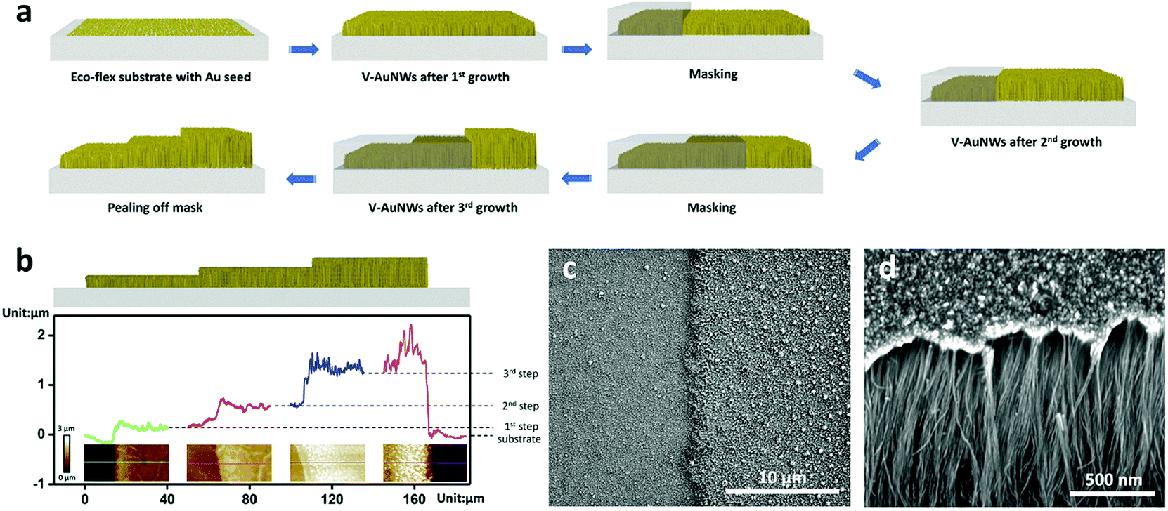 | ||
| Fig. 1 Fabrication and characterization of staircase-like vertically-aligned gold nanowire (V-AuNW) films. (a) Schematic of the fabrication process of the staircase V-AuNWs film. (b) Top: Cross-sectional schematic diagram of 3-step V-AuNWs film; middle: AFM images of the boundary areas of a 3-step V-AuNWs film; bottom: the corresponding height profiles for each AFM image. (c) The top-view SEM image of the boundary area of the V-AuNWs film. (d) The cross-sectional SEM image of the V-AuNWs film. | ||
The staircase morphology of V-AuNWs film is confirmed by atomic force microscopy (AFM) and scanning electron microscopy (SEM). Fig. 1b shows the AFM images and the corresponding line scan profiles of a three-step staircase V-AuNWs film. The step heights for the first, second and third staircase are ∼0.35 μm, ∼0.48 μm and ∼0.71 μm, respectively. The overall height of the 3rd-step V-AuNW layer to the Ecoflex substrate is estimated from the AFM line scan profile to be ∼1.5 μm. The staircase structures are further confirmed by SEM characterization (Fig. 1c and Fig. S8 in ESI†). The cross-sectional SEM image of the V-AuNWs clearly demonstrates enokitake-like standing nanowire structures at each step (Fig. 1d). It should be noted that such unique staircase-like structures have not been reported in previous gradient films.19,20,24,25 The time-controllable nanowire heights in conjunction with PI masking allow for the precise fabrication of staircase conducting films with well-defined hierarchical structures.
Then, we thoroughly investigated the electrical conductivities of V-AuNWs films of different thickness. 10 V-AuNWs film (1 × 1 cm2) samples were fabricated on spun-coated Ecoflex on glass substrates by programming the growth time from 1 to 10 minutes. The 1 min growth V-AuNWs film has a sheet resistance of 2959 ± 586 Ω. As the nanowire growth time gradually increases, the sheet resistance quickly decreases initially, but almost reaches a steady resistance after 7 minutes of growing time (Fig. S9a in ESI†). With 10 minutes’ growth, a typical sheet resistance of 10.5 ± 3.9 Ω is obtained. The sheet resistances for all 10 samples reduced further once the Ecoflex was peeled off the glass substrates. Typically, the electrical resistances of wrinkled V-AuNWs film with growing times from 1 to 10 minutes range from 1728 ± 225 Ω to 8.4 ± 3.7 Ω. This may be attributed to shrinkage of the Ecoflex after releasing it from the glass substrate, which tightens the nanowire packing and causes the V-AuNWs to wrinkle, as can be seen from optical characterizations (Fig. S9b–i in ESI†). Furthermore, the electrical responses of V-AuNWs samples with growing times of 1–10 minutes were recorded under a constant pressure (Fig. S10a in ESI†). Note that the pressure sensitivity of V-AuNWs films reduces as the nanowires get longer, but reaches a steady value after 7 minutes (Fig. S10b in ESI†). The reduced sensitivity is due to a lower base resistance as the nanowires get longer (Fig. S9a in ESI†).
Using the antiparallel back-to-back assembly of two staircase V-AuNWs, we demonstrate its location-specific sensing capability. As shown in Fig. 2a, we fabricated two V-AuNWs sensor strips (30 × 5 mm2) on Ecoflex substrates with anti-directional 6-step staircase structures (5 × 5 mm2 for each staircase) with growing times at one-minute intervals. Due to the variation in thickness, the conductivity changes along the longitudinal dimension exhibited opposite directions for the front (sensor 1) and back (sensor 2) sensors (Fig. 2b). Consequently, the overall increase in resistance of the two strips subjected to loads at different steps enables the accurate calculation of both the applied load and its location along the sensing strip.19
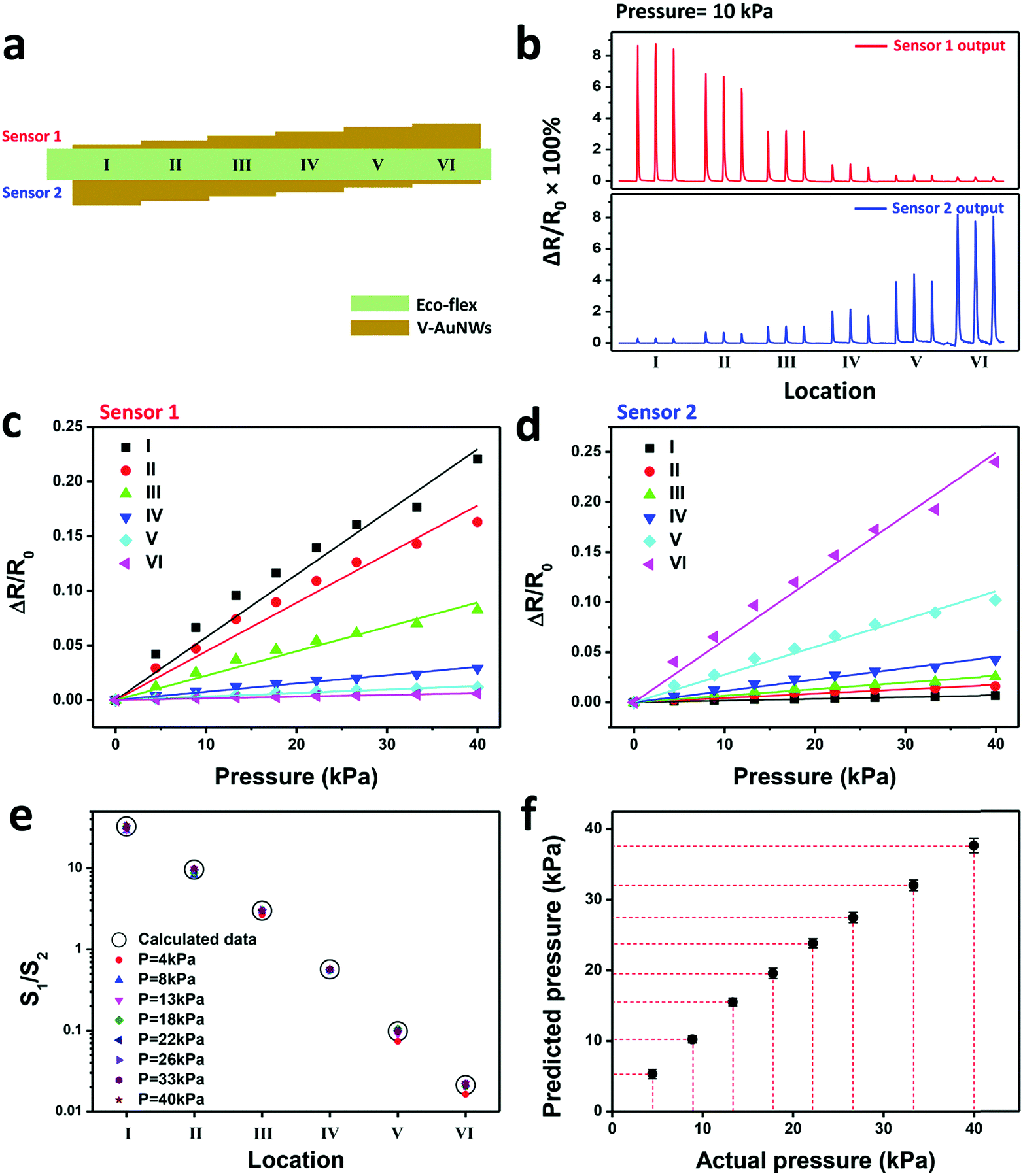 | ||
| Fig. 2 A linear location-specific sensor with an antiparallel V-AuNW thickness staircase. (a) Schematic of the linear location-specific sensor. (b) Location-specific pressure-sensing performances for the sensor 1 (red) and sensor 2 (blue) under a normal pressure of 10 kPa. (c and d) The relationship between changes in electrical resistance and location-specific pressures applied for locations I to VI. Solid lines are the linear fitting. (e) Correlations between the predicted and experimentally measured location-specific dimensionless parameter, Ln, for a pressure range from 4 to 40 kPa. (f) Correlations between the predicted pressures versus the actual pressure applied. The calculation was based on linear fitting curves for locations I to VI from sensor 1. | ||
In detail, we record the changes in resistance for sensor 1 and sensor 2 from the responses at each location (I to VI) to a constant pressure (Fig. 2c and d). In the calibration process, linear fits are adjusted at each specific location, giving a set of 6 linear fits for sensors 1 and 2. The pressure sensitivity S for each location can be defined as the slope of the traces.
We assume that a six-step staircase film could be regarded as six resistors connected in series. When a constant pressure P is applied on the nth-step, its sensitivity is defined as:
 | (1) |
 is the sum of the resistances at each step under no pressure, and ΔRn is the relative change in electrical resistance of the nth-step.
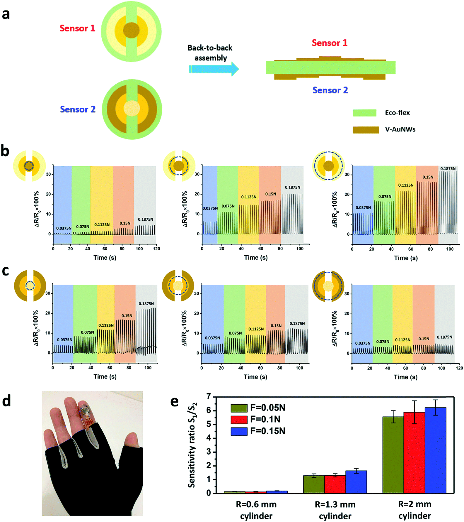
The location-specific dimensionless parameter Ln, namely the sensitivity ratio of sensors 1 and 2 (Sn1/Sn2) at step n could be defined as:
 | (2) |
The relationship between the pressed location and Ln is shown in Fig. 2e, where a calculated value of the sensitivity ratio is obtained for each location based on the linear fittings in Fig. 2c and d. The location specificity agrees well with the calculated value over a wide range of pressures (4–40 kPa). Next, we tested the pressure specificity of sensor 1 by comparing the real value of the load and the calculated value of the load. Fig. 2f shows that these values are nearly identical between 0 and 40 kPa. Therefore, a V-AuNWs sensor can be used to accurately measure both the pressure and the location of the applied force.
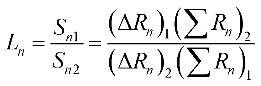
Remarkably, the location-specific pressure-sensing capability can be maintained even when the sensor is deformed. As shown in Fig. 3a, the sensor strip is subjected to 50% uniaxial elongation. The sensitivity ratio of sensors 1 and 2 from location I to location VI is demonstrated in Fig. 3b, and is independent of the applied pressure. The overall resistance of the staircase film is increased with an increase in strain level from 0% to 50% (Fig. S11 in ESI†), due to the generation of strain-induced cracks in each step of the film (Fig. S12 in ESI†). In addition, larger gaps and cracks are observed with thicker V-AuNWs steps (Fig. S12 in ESI†), leading to greater losses in conductivity compared to thinner V-AuNWs steps. Accordingly, the conductivity disparity between adjacent steps becomes smaller. As a result, the thicker V-AuNWs steps (locations IV, V, VI of sensor 1) are more responsive to pressure than thinner nanowire locations (location I, II, III of sensor 1) with the increasing level of strain (Fig. 3c and d).
 | ||
| Fig. 3 A linear location-specific sensor in the stretched state. (a) Schematic of a location-specific sensor under a uniaxial strain of 50%. (b) Correlations between the predicted and experimentally measured location-specific dimensionless parameter, Ln, when a 50% strain was applied. (c) Resistive responses for location I and location V of sensor 1 as a function of pressure with different levels of applied strain: 0%, 10%, 30% and 50%. (d) Location-specific sensitivity of sensor 1 under various strains: 0%, 10%, 30% and 50%. | ||
The location-specific sensor design can also be extended to other topological structures, such as a spiral pattern (Fig. S13a in ESI†). When pressure was applied to a sheet of the 2D sensor platform, the top and bottom staircase V-AuNWs sensors responded to the strain with variable resistances (Fig. S13b in ESI†). According to the collected database in Fig. 2, the actual position and pressure of a force could be well predicted with high accuracy.
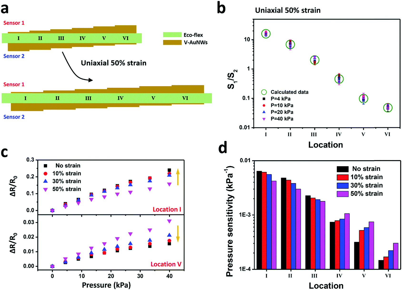
We further extended our design to concentric circle patterns to check whether a sharp or blunt object can be discriminated. The schematic design of the pressure area sensor is illustrated in Fig. 4a. Firstly, two concentric circle films with three-step staircase V-AuNWs were fabricated with variations in antiparallel thickness. The radii of the circles from inside to outside are 0.8 mm, 1.5 mm and 2.2 mm, respectively. The thickness of each circle is controlled by the growing time of the V-AuNWs at 2 minute intervals from 2 minutes to 6 minutes. The device is integrated by a back-to-back assembly of two antiparallel staircase films with a protective Ecoflex layer in between. Theoretically, the concentric circle pattern could be regarded as five resistors connected in series (Fig. S14a in ESI†). In addition, due to the low Young's modulus of soft Ecoflex thin film, stress concentration will occur in the edge area when the film is subjected to a uniform pressure (Fig. S14b–d in ESI†). Owing to the discrepancy in thickness for each circle between the top and bottom films, the top sensor is more responsive to a larger pressure area, as stresses are mostly concentrated in the outside thinner circle; while the bottom sensor is more sensitive to a smaller pressure area where the inside thinner circle is activated.
 | ||
| Fig. 4 Concentric design of antiparallel staircase sensors for sharpness detection. (a) Schematic of the staircase concentric sensor structural design. (b) Resistive responses of sensor 1 to cylinders with radii of 0.6 mm, 1.3 mm and 2 mm (from left to right) under forces from 0.0375 to 0.1875 N. (c) Resistive responses of sensor 2 to cylinders with radii of 0.6 mm, 1.3 mm and 2 mm (from left to right) under forces from 0.0375 to 0.1875 N. (d) A photograph of a sharpness-specific sensor attached to a human fingertip. (e) Sharpness-specific parameter SR independent of the forces applied. | ||
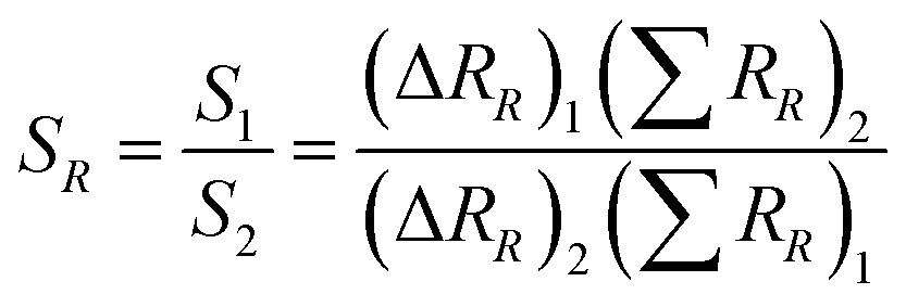
To evaluate the ability of our concentric circle sensors to detect sharpness, three cylinders with radii of 0.6 mm, 1.3 mm and 2 mm are utilized as probes. The force-dependent changes in resistance of the top and bottom sensors with the three cylindrical probes are demonstrated in Fig. 4b and c. The resistance of both sensors showed distinguishable signals to probes with different sizes over a wide range of forces from 0.0375 N to 0.1875 N, which could be used to evaluate the sharpness of the object. Note that the pressure area specificity is also demonstrated by pressure-dependent changes in the resistance of both sensors (Fig. S15 in ESI†), indicating that the ability of our system to resolve the contact area of objects is independent of the applied force or pressure. We further demonstrated the detection of sharpness by attaching wearable sensors integrated with a Bluetooth circuitry to human fingertips (Fig. 4d). Circular cone-shaped objects with various contact areas (0.75 cm2, 0.3 cm2 and 0.03 cm2) could be resolved (ESI,† Movie 2) by taping our sensors to the objects. The sharpness-specific dimensionless parameter SR, namely the sensitivity ratio of sensors 1 and 2 (S1/S2) pressed by cylinder with radius R could be defined as:
 | (3) |
 is the sum of resistances in each concentric circle under no pressure, and ΔRR is the relative change in electrical resistance when a force is applied by a cylinder with radius R. The relationship between SR and the cylinder radius R with applied forces of 0.05 N, 0.1 N and 0.15 N is illustrated in Fig. 4e, where specific values of the sensitivity ratio are obtained for cylinders with different contact areas.
From a practical standpoint, if the pressure is applied at the boundary of the staircase, complications may occur, interfering with our sharpness- and location-specific sensing concept. Nevertheless, we found that this can be avoided by applying a stiff encapsulation layer (e.g. polyethylene terephthalate, PET) on top of the V-AuNWs film (Fig. S16a and b in ESI†). The PET serves as a passivation material, preventing nanowire deformation when pressure is applied. Consequently, stiff PET sheets could cover the boundary areas of the staircase film to avoid problems in pressure/location detection at staircase boundaries (Fig. S16c, ESI†).
Conclusions
In conclusion, we report a location- and sharpness-specific tactile sensor based on staircase-like standing gold nanowires, which can substantially reduce the number of pixels required for soft pressure-sensing mapping. This is achieved because of accurate thickness control over the length of the standing gold nanowires and overall spatial topological structures – an ability which is difficult to achieve with traditional continuous metal films or nanomaterials. Notably, the entire device fabrication process is scalable without the need for complex and expensive equipment. Hence, our methodology represents a powerful low-cost strategy for fabricating skin-mimicking sensors that can be seamlessly integrated with soft human skin/muscles for biodiagnostics, anytime, anywhere.Experimental section
Materials
Gold(III) chloride trihydrate (HAuCl4·3H2O, 99.9%), triisopropylsilane (99%), 4-mercaptobenzoic acid (MBA, 90%), (3-aminopropyl) trimethoxysilane (APTES), sodium citrate tribasic dihydrate (99.0%), L-ascorbic acid, ethanol (analytical grade), sodium dodecylbenzenesulfonate (SDBS) and sodium borohydride (NaBH4) were purchased from Sigma-Aldrich. All solutions were prepared using deionized water (resistivity >18 MΩ cm−1). All chemicals were used as received unless otherwise indicated. Single wall carbon nanotubes (SWCNTs) were purchased from XFNANO INC with diameters of 1–2 nm and lengths of 5–30 μm. Conductive thread was purchased from Adafruit. PDMS substrates were made by mixing the prepolymer gel (Sylgard 184 Silicone Elastomer Base) and the cross linker (Sylgard 184 Silicone Elastomer Curing Agent) with a weight ratio of 10![[thin space (1/6-em)]](https://www.rsc.org/images/entities/char_2009.gif) :1. The mixture was spin coated on a glass slide at 300 rpm for 2 minutes and cured at 65 °C for 2 h in an oven. After curing, the PDMS sheet with a thickness of 300 mm was cut for further use.
:1. The mixture was spin coated on a glass slide at 300 rpm for 2 minutes and cured at 65 °C for 2 h in an oven. After curing, the PDMS sheet with a thickness of 300 mm was cut for further use.
Synthesis of 5 nm gold nanoparticles
0.147 ml of 34 mM sodium citrate was added into conical flask with 20 ml of H2O under vigorous stirring. After 1 min, 600 μl of ice-cold, freshly prepared 0.1 M NaBH4 solution was added under stirring. The solution turned brown immediately. The solution was stirred for 2 min and then stored at 4 °C until needed.Growth of vertically aligned gold nanowires (V-AuNWs)
Nanowires were grown on a stretchable Ecoflex substrate. Ecoflex substrates were made by pouring Ecoflex curable silicone fluid (Smooth-On Ecoflex 00-30) onto a 3′′ glass slide, followed by spin coating the fluid at a speed of 500 rpm for 1 minute and curing at room temperature for 1 hour. After solidification, the as-fabricated Ecoflex film (∼200 μm in thickness, confirmed by optical microscopy) was pretreated with air plasma for 12 minutes to improve its surface hydrophilicity. The film was then functionalized with an amino group by reacting with APTMS solution (5 mM) for 1 h. Subsequently, the Ecoflex film was soaked in excess citrate-stabilized Au seed (3–5 nm) solution for 2 hours to ensure the adsorption of Au seeds and rinsed with water 10 times to remove the excess Au seeds. Then, the Au seed modified substrates were floated onto the surface of the growth solution (10 ml) with the APTMS-functionalized side facing downward in the solution for the uniform growth of V-AuNWs without the formation of any precipitates. The V-AuNWs growth solution contained ligand MBA (550 μM), HAuCl4 (6.8 mM), and L-ascorbic acid (16.4 mM). Finally, the V-AuNWs film was rinsed with ethanol 3 times and dried naturally.Fabrication of spiral staircase V-AuNWs strip
The spiral shape was predefined by a PI tape mask on an Ecoflex substrate with a width of 5 mm and an aspect ratio of 40. Then a similar growing-masking-growing process was repeated to obtain a 9-step staircase V-AuNWs film with growing times from 1 to 9 minutes at 1 minute intervals.Fabrication of concentric staircase V-AuNWs film
The extended electrodes were pre-defined by a PI tape mask and grown on an Ecoflex substrate with a growing time of 5 minutes. Then the growing-masking-growing process was repeated to obtain a 3-step concentric circle staircase V-AuNWs film with growing times from 2 to 6 minutes at 2 minute intervals. The radii for three concentric patterns are 0.8 mm, 1.5 mm and 2.2 mm, respectively. Two such films with an antiparallel staircase were then adhered back to back with a protective Ecoflex layer in between.Fabrication of gold film and carbon nanotube film on Ecoflex
The gold film (50 nm) was deposited onto an Ecoflex substrate at a speed of 0.3 nm s−1 by an electron beam evaporator (Intlvac Nanochrome II, 10 kV). The SWCNT solution was prepared with sodium dodecylbenzenesulfonate (SDBS) as a surfactant, where the concentrations of SDBS and SWCNT were 10 and 1 mg ml−1 in DI water. After bath sonication for 5 min, the CNT dispersion was probe-sonicated for 30 min at 200 W (VC 505; Sonics) to form an ink. A commercial airbrush (Airbrush Outfit) was used to spray coat the CNT ink at a distance of 10 cm. Uniform black CNT films were produced after multiple passes of the airbrush. The film was further placed in a vacuum oven at 100 °C for 1 h to remove residual solvent.Characterization
The scanning electron microscopy (SEM) image was characterized using FEI Helios Nanolab 600 FIB-SEM operating at a voltage of 5 kV. Atomic force microscopy (AFM) was characterized by the Dimension Icon AFM using ScanAsystTM imaging mode. To test the electro-mechanical responses of our pressure sensors, a piezoelectric stepping positioner (SLC-1730) with various probes was controlled by a custom LabView program to apply an external pressure up to 40 kPa. The pressure data was measured by a force sensor attached to the stepping positioner (ATI Nano17 Force/Torque Sensor, 1/80N resolution without filtering). Probes with different contact areas were designed using 3DS MAX and fabricated by an Objet Eden 260V 3D printer. To test the electrical responses of the sensors with pre-strain, two ends of the sample were attached to a motorized moving stage (THORLABS Model LTS150/M) to a desired strain, while the pressure responses were characterized as mentioned above. The electrical resistance responses for the pressure sensor were recorded by the Parstat 2273 electrochemical system (Princeton Applied Research). The sheet resistances of the V-AuNWs film were studied on a Jandel four-point conductivity probe by using a linearly arrayed four-point head.Conflicts of interest
There are no conflicts to declare.Acknowledgements
This work is financially supported by ARC projects DP180101715 and LP160100521. This work was performed in part at the Melbourne Centre for Nanofabrication (MCN) in the Victorian Node of the Australian National Fabrication Facility (ANFF).Notes and references
- A. Chortos, J. Liu and Z. Bao, Nat. Mater., 2016, 15, 937–950 CrossRef PubMed.
- D. H. Kim, N. Lu, R. Ma, Y. S. Kim, R. H. Kim, S. Wang, J. Wu, S. M. Won, H. Tao, A. Islam, K. J. Yu, T. I. Kim, R. Chowdhury, M. Ying, L. Xu, M. Li, H. J. Chung, H. Keum, M. McCormick, P. Liu, Y. W. Zhang, F. G. Omenetto, Y. Huang, T. Coleman and J. A. Rogers, Science, 2011, 333, 838–843 CrossRef PubMed.
- M. Kaltenbrunner, T. Sekitani, J. Reeder, T. Yokota, K. Kuribara, T. Tokuhara, M. Drack, R. Schwödiauer, I. Graz, S. B. Gogonea, S. Bauer and T. Someya, Nature, 2013, 499, 458–463 CrossRef PubMed.
- T. Someya, Z. Bao and G. G. Malliaras, Nature, 2016, 540, 379–385 CrossRef PubMed.
- S. Gong, W. Schwalb, Y. Wang, Y. Chen, Y. Tang, J. Si, B. Shirinzadeh and W. Cheng, Nat. Commun., 2014, 5, 3132–3138 CrossRef PubMed.
- S. Lee, A. Reuveny, J. Reeder, S. Lee, H. Jin, Q. Liu, T. Yokota, T. Sekitani, T. Isoyama, Y. Abe, Z. Suo and T. Someya, Nat. Nanotechnol., 2016, 11, 472–478 CrossRef PubMed.
- D. Lipomi, M. Vosgueritchian, B. C. K. Tee, S. L. Hellstrom, J. A. Lee, C. H. Fox and Z. Bao, Nat. Nanotechnol., 2011, 6, 788–792 CrossRef PubMed.
- C. Pang, G. Y. Lee, T. I. Kim, S. M. Kim, H. N. Kim, S. H. Ahn and K. Y. Suh, Nat. Mater., 2012, 11, 795–801 CrossRef PubMed.
- T. Sekitani, Y. Noguchi, K. Hata, T. Fukushima, T. Aida and T. Someya, Science, 2008, 321, 1468–1472 CrossRef PubMed.
- K. Takei, T. Takahashi, J. C. Ho, H. Ko, A. G. Gillies, P. W. Leu, R. S. Fearing and A. Javey, Nat. Mater., 2010, 9, 821–826 CrossRef PubMed.
- H. B. Yao, J. Ge, F. F. Wang, X. Wang, W. Hu, Z. J. Zheng, Y. Ni and S. H. Yu, Adv. Mater., 2013, 25, 6692–6698 CrossRef PubMed.
- M. Melzer, M. Kaltenbrunner, D. Makarov, D. Karnaushenko, D. Karnaushenko, T. Sekitani, T. Someya and O. G. Schmidt, Nat. Commun., 2015, 6, 6080–6087 CrossRef PubMed.
- A. Alfadhel and J. Kosel, Adv. Mater., 2015, 27, 7888–7892 CrossRef PubMed.
- C. Wang, D. Hwang, Z. Yu, K. Takei, J. Park, T. Chen, B. Ma and A. Javey, Nat. Mater., 2013, 12, 899–904 CrossRef PubMed.
- X. Wang, M. Que, M. Chen, X. Han, X. Li, C. Pan and Z. L. Wang, Adv. Mater., 2017, 29, 1605817 CrossRef PubMed.
- T. Yamada, Y. Hayamizu, Y. Yamamoto, Y. Yomogida, A. I. Najafabadi, D. N. Futaba and K. Hata, Nat. Nanotechnol., 2011, 6, 296–301 CrossRef PubMed.
- V. Maheshwari and R. F. Saraf, Science, 2006, 312, 1501–1504 CrossRef PubMed.
- C. L. Choong, M. B. Shim, B. S. Lee, S. Jeon, D. S. Ko, T. H. Kang, J. Bae, S. H. Lee, K. E. Byun, J. Im, Y. J. Jeong, C. E. Park, J. J. Park and U. I. Chung, Adv. Mater., 2014, 26, 3451–3458 CrossRef PubMed.
- M. S. Bar, G. Konvalina and H. Haick, Adv. Mater., 2015, 27, 1779–1784 CrossRef PubMed.
- Y. Tai and G. Lubineau, Adv. Funct. Mater., 2016, 26, 4078–4084 CrossRef.
- J. He, Y. Wang, Y. Feng, X. Qi, Z. Zeng, Q. Liu, W. S. Teo, C. L. Gan, H. Zhang and H. Chen, ACS Nano, 2013, 7, 2733–2740 CrossRef PubMed.
- S. Gong, D. T. H. Lai, B. Su, K. J. Si, Z. Ma, L. W. Yap, P. Guo and W. Cheng, Adv. Electron. Mater., 2015, 1, 1400063 CrossRef.
- S. Gong, D. T. H. Lai, Y. Wang, L. W. Yap, K. J. Si, Q. Shi, N. N. Jason, T. Sridhar, H. Uddin and W. Cheng, ACS Appl. Mater. Interfaces, 2015, 7, 19700–19708 CrossRef PubMed.
- Z. Liu, D. Qi, P. Guo, Y. Liu, B. Zhu, H. Yang, Y. Liu, B. Li, C. Zhang, J. Yu, B. Liedberg and X. Chen, Adv. Mater., 2015, 27, 6230–6237 CrossRef PubMed.
- Z. Lin, X. Gui, Z. Zeng, B. Liang, W. Chen, M. Liu, Y. Zhu, A. Cao and Z. Tang, Adv. Funct. Mater., 2015, 25, 7173–7179 CrossRef.
Footnotes |
| † Electronic supplementary information (ESI) available: Experimental section, supporting figures and videos. See DOI: 10.1039/c8nh00125a |
| ‡ These two authors contribute equally to this work. |
| This journal is © The Royal Society of Chemistry 2018 |