
High-temperature driven inter-valley carrier transfer and significant fluorescence enhancement in multilayer WS2†
Heyu
Chen
a,
Yuanzheng
Li
a,
Weizhen
Liu
*ab,
Haiyang
Xu
 *a,
Guochun
Yang
a,
Jia
Shi
c,
Qiushi
Feng
a,
Tong
Yu
a,
Xinfeng
Liu
c and
Yichun
Liu
a
*a,
Guochun
Yang
a,
Jia
Shi
c,
Qiushi
Feng
a,
Tong
Yu
a,
Xinfeng
Liu
c and
Yichun
Liu
a
aCentre for Advanced Optoelectronic Functional Materials Research and Key Laboratory of UV-Emitting Materials and Technology (Northeast Normal University), Ministry of Education, Changchun 130024, China. E-mail: hyxu@nenu.edu.cn
bNational Demonstration Center for Experimental Physics Education (Northeast Normal University), Changchun 130024, China. E-mail: wzliu@nenu.edu.cn
cDivision of Nanophotonics, CAS Key Laboratory of Standardization and Measurement for Nanotechnology, CAS Center for Excellence in Nanoscience, National Center for Nanoscience and Technology, Beijing 100190, China
First published on 29th June 2018
Abstract
It is quite necessary to understand and control the essential carrier dynamic behaviors of two-dimensional WS2, which is regarded as a very promising material for integrated nanoelectronic and optoelectronic devices. Herein, a high-temperature driven carrier transfer process of multilayer WS2 nanoflakes is proposed. The established model, involving the inter-valley transfer process of photocarriers from the Λ/Γ point to the K point, predicts the significant emission enhancement of the K → K direct transition at high temperatures, which is verified by both theoretical calculations and experimental observations. On the one hand, variations in the estimated population ratio of photo-carriers with increasing temperature well support the proposed model. On the other hand, temperature-dependent photoluminescence spectra clearly show that the K → K direct emission intensity is remarkably enhanced by ∼300-fold as the temperature is elevated to 760 K. Time-resolved fluorescence spectral studies confirm the occurrence of the inter-valley carrier transfer process in the multilayer WS2. These results provide solid evidence for the proposed inter-valley carrier transfer model. Such a mechanism could not only be applied to improve the luminescence intensity of indirect-band-gap semiconductors, but also be further extended to design optoelectronic devices which have special requirements on controlling the carrier dynamic behavior.
Conceptual insightsTransition metal dichalcogenides (TMDs) hold great promise for technological applications in the fields of nanoelectronics and optoelectronics, owing to their superior electronic and optical properties. Multilayer TMDs have many notable superiorities over their monolayer counterparts such as higher electron mobility, stronger photon absorption ability and larger optical density of states. Therefore, it is essentially important to improve the optical performance of ML-TMDs and understand their excited-state carrier dynamics, which may pave the way for future exploration of ML-TMD-based optoelectronic devices. However, research reports on ML-TMDs are relatively rare in comparison with those on their monolayer counterparts. Herein, a remarkable high-temperature-induced fluorescence emission enhancement (∼300-fold) from ML-WS2 nanoflakes is observed for the first time. A theoretical model involving thermo-driven inter-valley transfer of photocarriers is proposed that explains this intriguing phenomenon. Population ratio calculations and multiple spectral characterization (temperature-dependent and time-resolved spectra) confirm the validity and reliability of this established inter-valley transfer model. The present study not only suggests a general strategy to enhance the luminescence performance of indirect-band-gap semiconductors but also sheds more light on the carrier dynamic mechanism of 2D materials, both of which are very important to develop new-type electronic and photonic devices based on these emerging materials. |
Introduction
Transition metal dichalcogenides (TMDs) hold great promise for technological applications in various fields including tunneling transistors, photodetectors, LEDs and flexible electronics, owing to their superior electronic and optical properties.1–8 Among them, MoS2, as a typical representative for TMDs, has attracted the most attention due to its relatively easy availability through mechanical exfoliation or chemical vapor deposition. On the other hand, closely related WS2 is quickly attracting extensive interest as well.5–11 Recently, WS2 with a similar layered structure to MoS2 has been found to exhibit a finite band-gap in the visible wavelength range.3,11–13 In addition, compared with MoS2, monolayer WS2 has a superior luminescence quantum efficiency and a larger spin–orbit coupling strength, suggesting that it may exhibit larger band edge splitting and a stronger magnetic coupling effect.5,6,14–17 These merits could lead to the realization of high-performance optoelectronic and spintronic devices based on two-dimensional (2D) WS2 materials.17–19It should be noted that the optical properties of TMDs vary significantly with layer thickness.11,13 Monolayer WS2 is a direct band-gap semiconductor with a band-gap value of ∼2.0 eV. However, it exhibits an indirect band-gap of ∼1.4 eV in the multilayer (ML) configuration and shows a markedly suppressed fluorescence quantum yield.9,15 Obviously, the indirect-band-gap nature of ML-TMDs limits their applications in optoelectronic devices such as LEDs, photodetectors and lasers. In fact, ML samples have many notable superiorities over their monolayer counterparts such as higher electron mobility, stronger photon absorption ability and larger optical density of states.20–22 Therefore, it is essentially important to improve the optical performance of ML-TMDs and understand their excited-state carrier dynamics, which may pave the way for future exploration of ML-TMD-based optoelectronic devices. However, research reports on the ML-TMDs are relatively rare in comparison with those on their monolayer counterparts.
In this work, the high-temperature carrier dynamics of ML-WS2 have been theoretically studied according to the Boltzmann distribution law. The population ratio of electrons and holes in different energy valleys and hills and its variation with increasing temperature are carefully examined. Furthermore, a significant fluorescence emission enhancement at high temperatures is expected on the basis of these theoretical analyses, and is indeed observed for the first time in subsequent temperature-dependent PL experiments. Time-resolved spectral measurements confirm that high-temperature-induced inter-valley transfer of photocarriers should be responsible for the observed PL variations. The current research not only provides an effective method for improving the luminescence performance of indirect-band-gap ML-TMDs, but also deepens the understanding of the excited-state carrier dynamics in the TMD material family.
Results and discussion
Fig. 1(a) illustrates the ball-and-stick structural model of a ML-WS2 nanoflake. Each molecular layer comprises two hexagonal planes of S atoms and an intermediate hexagonal plane of W atoms. The W atoms coordinate with the S atoms through ionic–covalent bond interactions in a trigonal prismatic manner.11,23 Environmental temperature has a huge impact on the physical properties of semiconductors. In general, the number of phonons will increase due to stronger lattice vibrations with increasing temperature, which may induce some intriguing carrier dynamic behaviors and optical phenomena. Therefore, heating is usually considered as a simple and efficient strategy to tune the optical properties of materials. In the current case, a high-temperature-driven carrier transfer process, termed as inter-valley transfer of photo-carriers, is expected to occur in the ML-WS2 sample. Fig. 1(b) illustrates the specific carrier transfer process in the energy band diagram of a ML-WS2 nanoflake. It has been proved that conduction band valleys of ML-WS2 are located at the Λ and K points of the Brillouin zone, while valence band hills are located at the Γ and K points.3,23,24 In particular, the conduction band minimum (CBM) and valence band maximum (VBM) of ML-WS2 are respectively situated at the Λ valley for electrons and the Γ hill for holes, indicating the indirect-band-gap feature of ML-WS2. Therefore, most photo-carriers would occupy the Λ valley and the Γ hill at room temperature. However, when the temperature increases, excited-state electrons and holes will gain extra energy from the surrounding crystal lattices as a result of the intensified carrier–phonon interaction.25 Thus, as indicated by the orange arrows in Fig. 1(b), the electrons obtaining sufficient kinetic energy will transfer from the Λ valley to the K valley, while the holes with greatly improved kinetic energy will also experience a similar transfer from the Γ hill to the K hill. Through this process, more electrons and holes will occupy the K valley and the K hill at high temperatures.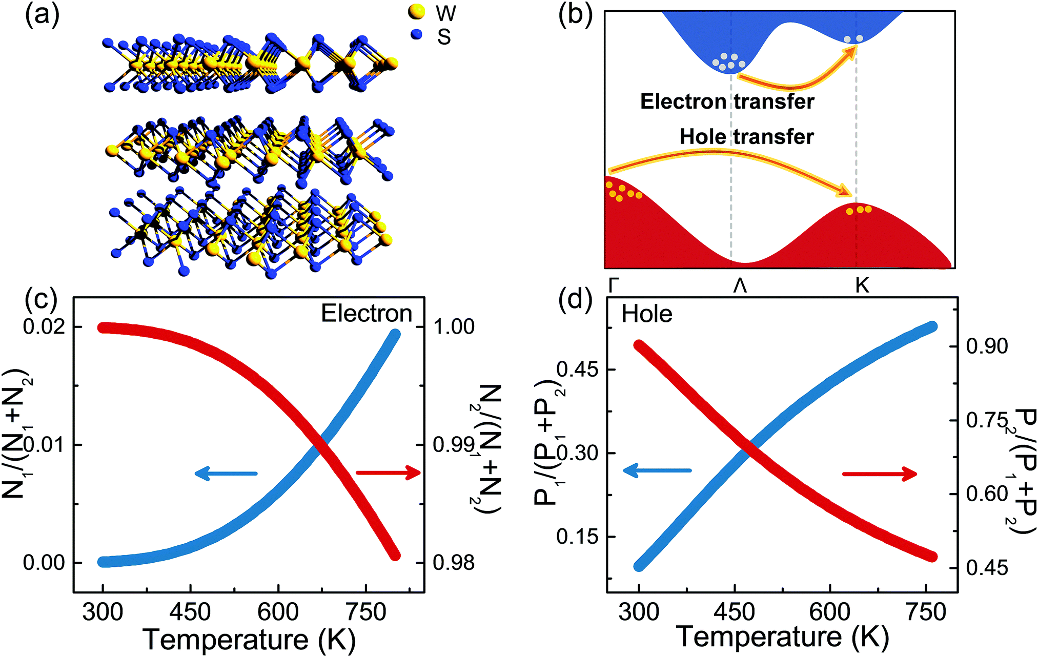 | ||
| Fig. 1 (a) Structural schematic diagram of a multilayer 2H-WS2 sample. (b) A scheme showing the transfer process of photo-carriers among different energy valleys and hills; the orange arrows indicate the transfer direction from Λ/Γ to K. Population ratio of the electrons (c) and holes (d) in the K point (blue curve) and the Λ/Γ point (red curve) as a function of the measurement temperature in ML-WS2. | ||
In order to verify this proposed transfer model, both theoretical analyses and experimental studies have been carried out. First, a rough estimation of the temperature-dependent carrier population ratio among different energy valleys and hills is conducted according to the Boltzmann distribution law. The relevant results are illustrated in Fig. 1(c) and (d) (see Note 1 of the ESI† for calculation details). It could be seen in Fig. 1(c) that the population ratio of the electrons at the K valley N1/(N1 + N2) (herein, N1 and N2 correspond to the electron numbers at the K valley and Λ valley, respectively) shows a rapid increasing trend as the temperature increases. In contrast, the electron occupation ratio at the Λ valley N2/(N1 + N2) decreases monotonously with increasing temperature. Similarly, the population ratio of the holes at the K hill P1/(P1 + P2) increases, whereas that at the Γ hill P2/(P1 + P2) declines when the temperature is elevated (see Fig. 1(d); P1 and P2 stand for the hole numbers at the K hill and Γ hill, respectively). More specifically, the above estimations demonstrate that the population ratio of photo-carriers at the K point (including the K-valley and K-hill) is improved ∼1000-fold when the environmental temperature is increased from 300 to 760 K. The opposite change tendency of the population ratio at the K point and the Λ/Γ point implies that inter-valley carrier transfer could occur theoretically as the temperature continuously increases. In such a case, the number of excited-state carriers at the K point will be largely increased, which may significantly enhance the emission intensity of the K → K direct transition of ML-WS2.
To experimentally examine whether the fluorescence emission intensity of ML-WS2 is improved or not, temperature-dependent PL (TD-PL) measurements from 300 to 760 K are performed for mechanically exfoliated ML-WS2 flakes. Fig. 2(a) shows an atomic force microscopy (AFM) image of an exfoliated ML-WS2 flake with a thickness of ∼18.5 nm, corresponding to ∼23 layers. To prevent the sample from being oxidized at high temperatures, high-purity argon is employed as a shielding gas during the whole PL measurement procedure. Fig. 2(b) shows the TD-PL spectra of this ML-WS2 sample. As an indirect-band-gap semiconductor, the PL intensity of ML-WS2 is usually very low. Only a weak emission peak with a broad linewidth is observed at ∼870 nm when the temperature is below 400 K.
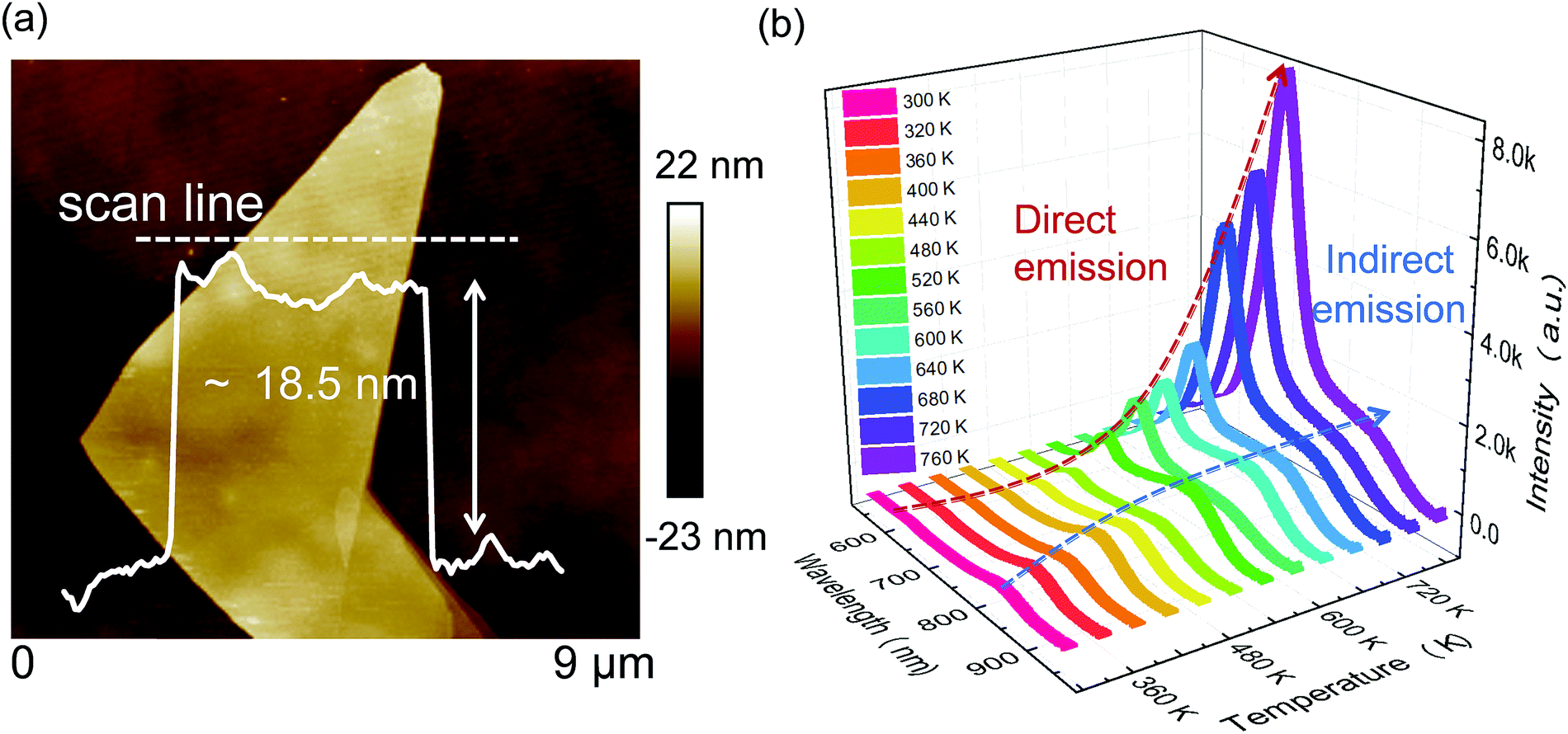 | ||
| Fig. 2 (a) A typical AFM image showing the height profile of the mechanically exfoliated ML-WS2 flake. (b) Steady-state TD-PL spectra of the ML-WS2 sample taken at a temperature range of 300–760 K; the red and blue dashed arrows respectively indicate the variations of direct and indirect emission peaks with temperature. | ||
This weak PL signal can be attributed to the indirect-band-gap transitions in ML-WS2, because indirect emissions generally show very low quantum yields.26 As the measurement temperature increases to 440 K, another PL peak appears at ∼690 nm, corresponding to the K → K direct transition emission of ML-WS2. The above assignments of the PL peaks will be discussed in detail in Fig. 3. Further increasing the temperature leads to the PL intensity improvement for both peaks, but the short-wavelength direct emission shows a more rapid increase rate than the long-wavelength indirect emission. After 560 K, the PL intensity of the direct emission is higher than that of the indirect emission. The entire PL spectrum is dominated by the direct emission at a high temperature of 760 K. To avoid the thermo-induced sample destruction or defect formation caused by atom evaporation, the measurement temperature is not further elevated. The TD-PL spectra of other ML-WS2 samples with different thicknesses are also tested, and similar high-temperature-induced fluorescence emission enhancements are observed (see Fig. S1 of the ESI†), confirming the reliability and reproducibility of this intriguing luminescence phenomenon.
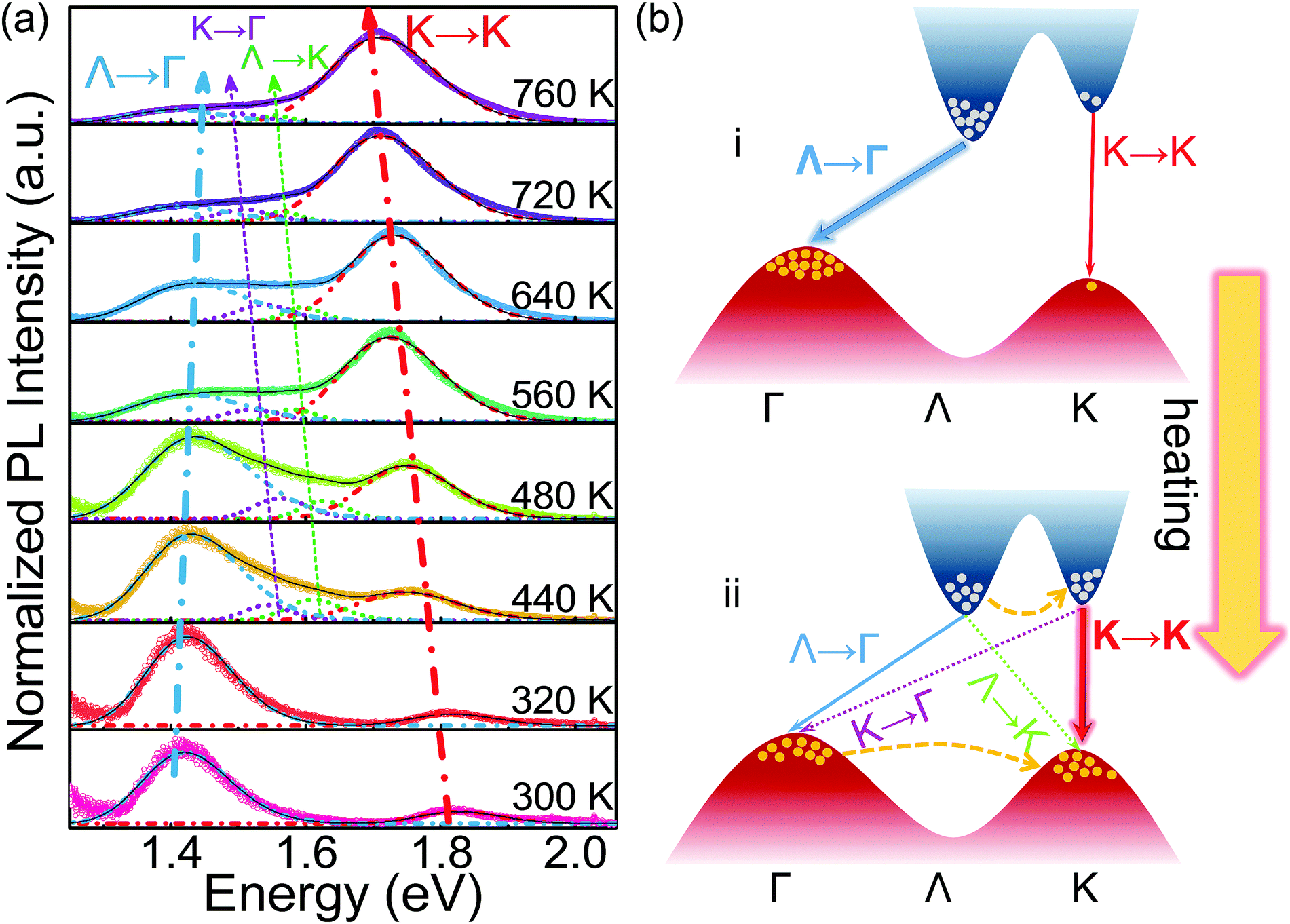 | ||
| Fig. 3 (a) Multi-peak deconvolution fittings of the TD-PL spectra, showing the specific variation of each sub-peak at different temperatures. (b) Schematic diagram illustrating the excited-state carrier distribution and possible radiative transition routes at (i) room temperature and (ii) high temperature; the carrier population at the K point is effectively increased due to the heat-induced inter-valley transfer process in panel (ii). | ||
It is noteworthy that the vast majority of previous reports on 2D materials mainly focus on monolayer or few-layer (e.g. bilayer or trilayer) flakes, which are usually grown by chemical vapor deposition or other physical/chemical methods. Herein, we pay attention to the luminescence properties of multilayer (>10-layer) WS2 samples with different thicknesses. To easily obtain these multilayer samples, a simple mechanical exfoliation method is adopted. Honestly speaking, the mechanical exfoliation approach does not have good control over the sample thickness. However, it is still able to produce experimental specimens with large thickness difference via a multi-cycle peeling process. In the current work, three multilayer WS2 flakes with distinctly different thicknesses of 18.5 nm (∼23-layer and <50-layer), 54 nm (∼68-layer and >50-layer) and 120 nm (∼150-layer and >100-layer) are intentionally created, to confirm that the heating-triggered luminescence enhancement phenomenon could happen in multilayer WS2 samples with distinctly different thicknesses. As expected, similar fluorescence emission enhancements at elevated temperatures are observed from all these samples (see Fig. S1 of the ESI†), indicating the validity of the proposed inter-valley carrier transfer model for multilayer WS2 samples.
For better analyzing these TD-PL spectra, Gaussian deconvolution multi-peak fittings are performed, and the relevant results are shown in Fig. 3(a). As can be seen, all spectra are mainly composed of two emission bands at different measurement temperatures. One is the indirect transition emission located at ∼1.42 eV at 300 K, originating from the Λ → Γ transition (see Fig. 3(b)). The other is the direct transition emission situated at ∼1.82 eV at 300 K, stemming from the K → K direct recombination. At a relatively low temperature of 300 K, the PL intensity of the Λ → Γ indirect emission is obviously higher than that of the K → K direct emission. This is because ML-WS2 is an indirect-band-gap semiconductor. Nearly all photo-excited electrons and holes are respectively populated at the CBM (Λ valley) and the VBM (Γ hill) at room temperature. Therefore, only the Λ → Γ indirect emission can be observed, whereas the K → K direct emission, with a just detectable intensity, is extremely weak. With the increase of measurement temperature, the K → K emission intensity improves quickly and exceeds the Λ → Γ emission intensity at 560 K. At 760 K, the K → K direct emission peak dominates over the entire PL spectrum. As analyzed above, high temperatures induce a re-distribution of photo-carriers. More electrons and holes are transferred from the Λ/Γ point to the K point, which increases the carrier population fraction at the K point and thus enhances the K → K direct emission intensity.
It is noted in Fig. 3(a) that two additional K-point-related emission peaks (K → Γ transition and Λ → K transition, see Fig. 3(b)) are also activated at high temperatures owing to the increased K-point population ratio. In fact, the emergence of these two new peaks could be just viewed as a piece of clear evidence for the proposed carrier transfer model. Besides, the red shifts of the emission energy for the K-point-related transitions (K → K, K → Γ and Λ → K) are observed as the temperature rises. This is a common result for the TD-PL spectra of semiconductor materials, and could be attributed to the thermo-induced band-gap shrinkage effect.27–29 In the current case, the K valley moves downward and the K hill moves upward, reducing the K-point-related band-gap and emission energy at high temperatures.24,27 However, an interesting finding is that the Λ → Γ indirect transition displays an anomalous blue shift in emission energy. According to a previous theoretical calculation study,24 this may be because the Λ valley and the Γ hill would slightly depart from each other (upshift for the Λ valley, while downshift for the Γ hill) with increasing temperature. Such a variation will slightly enlarge the band-gap between the Λ valley and the Γ hill, resulting in a small increment in the Λ → Γ emission energy. A similar high-temperature causing a blue-shift phenomenon of the Λ → Γ transition in other TMDs has also been observed by Zhao et al.24
To clearly demonstrate the enhancement extent of the two main emissions, Fig. 4(a) shows the specific enhancement factor (FE) of the K → K direct and Λ → Γ indirect transitions at different temperatures. Herein, the enhancement factor FE is defined as the ratio between the K → K (or Λ → Γ) emission intensity (integrated) at elevated temperatures and that at room temperature. As is shown, a remarkable enhancement is observed for the K → K direct emission intensity by increasing the measurement temperature, and a ∼300-fold FE is obtained at 760 K. In contrast, the Λ → Γ indirect emission exhibits a negligible PL enhancement. The derived FE for the Λ → Γ emission is merely one percent of the enhancement factor for the K → K direct emission. This minute improvement of the Λ → Γ emission intensity could be ascribed to the strengthened electron–phonon (or electron–lattice) interaction at elevated temperatures, which facilitates the phonon-assisted indirect radiative transition.30,31Fig. 4(b) shows the temperature dependence of the integrated intensity ratio of the K → K direct emission to the Λ → Γ indirect emission (IK→K/IΛ→Γ), which can reflect the relative intensity variation of these two luminescent components. As can be seen, the IK→K/IΛ→Γ value demonstrates a monotonous increasing trend with temperature, indicating a much faster PL intensity increase rate of the K → K direct emission than that of the Λ → Γ indirect emission. This is consistent with the former analysis, further confirming the validity of our proposed carrier transfer mechanism. Herein, a comparison of the radiative recombination probability at the K point (PK) and the Λ/Γ point (PΛ/Γ) is made on the basis of the IK→K/IΛ→Γ value at 760 K (see Note 2 of the ESI† for detailed discussion). This comparison suggests that the PK of the K-point-related direct transition is generally one to two orders of magnitude higher than the PΛ/Γ of Λ/Γ-point-related indirect transitions, verifying the effectiveness of the K → K direct transition as a high-efficiency radiative recombination channel.
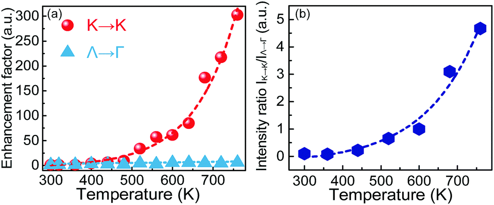 | ||
| Fig. 4 (a) Enhancement factor of the K → K direct and Λ → Γ indirect emissions at different temperatures. (b) Temperature dependence of the integrated intensity ratio of the K → K direct emission to the Λ → Γ indirect emission (IK→K/IΛ→Γ). | ||
Fig. 5(a) shows the time-resolved PL spectra of the K → K direct emission at different temperatures, which can directly reflect the temperature-dependent exited-state carrier dynamic process. As is shown, all transient-state spectra demonstrate a similar decay behavior with time, and could be well fitted by an exponential attenuation function: I = A![[thin space (1/6-em)]](https://www.rsc.org/images/entities/char_2009.gif) exp(−t/τ) + I0. Herein, τ is the effective lifetime of the K-point photo-carriers; A and I0 are two fitting parameters (see Note 3 of the ESI† for detailed fitting results). As can be deduced from the fitting equation, I is equal to I0 as the time τ approaches infinity. From this point of view, the fitting parameter I0 represents the residual fluorescence background signal after the effective emission intensity completely decays. The residual fluorescence background signal may come from the testing instrument response or ambient environment noise. Usually, the excited-state carriers can decay through both radiative (e.g. excitons/electron–hole-pairs radiative emission) and non-radiative (e.g. carrier–carrier scattering-induced Auger process or carrier–phonon scattering-induced lattice heating effect) recombination pathways.32–34 Hence, the τ derived here represents the overall depopulation situation of the K point carriers induced by the above radiative and non-radiative factors. Fig. 5(b) illustrates the variation trend of the τ value as a function of the measurement temperature. As can be seen, the τ value is ∼80 ps at 300 K, which is in good agreement with the reported carrier lifetime value in 2D WS2 materials.35,36 It is generally believed that the excited-state lifetime of semiconductors will decrease with increasing temperature, as a result of the strengthened carrier–phonon/carrier–carrier interactions or more thermally-activated non-radiative channels.37,38 However, it is observed that τ exhibits an abnormal uptrend from ∼80 to ∼120 ps when the measurement temperature is elevated from 300 to 680 K, which is inconsistent with the previous cognition. In fact, such an abnormal lifetime increase of the K point carriers could just prove the occurrence of inter-valley transfer at high temperatures, which shall be interpreted as follows. According to the proposed model, photo-carriers would transfer from the Λ/Γ point to the K point at elevated temperatures. Thanks to this transfer process, the K point carrier number is supplemented effectively and timely by these “newly injected” carriers from the Λ/Γ point, leading to the observed elongated lifetime of the K point carriers. In addition, because a considerable amount of these “newly injected” carriers participate in the radiative recombination process, the PL intensity of the K → K direct transition is significantly enhanced with increasing temperatures. Although the transient-state fluorescence characterization is unable to be performed on the Λ → Γ indirect emission due to the limited detection wavelength (300–800 nm) of the current spectroscopy system, the current experimental observations of the enhanced K → K emission intensity and the prolonged K-point excited-state lifetime at elevated temperatures have provided solid support to the proposed inter-valley carrier transfer model.
exp(−t/τ) + I0. Herein, τ is the effective lifetime of the K-point photo-carriers; A and I0 are two fitting parameters (see Note 3 of the ESI† for detailed fitting results). As can be deduced from the fitting equation, I is equal to I0 as the time τ approaches infinity. From this point of view, the fitting parameter I0 represents the residual fluorescence background signal after the effective emission intensity completely decays. The residual fluorescence background signal may come from the testing instrument response or ambient environment noise. Usually, the excited-state carriers can decay through both radiative (e.g. excitons/electron–hole-pairs radiative emission) and non-radiative (e.g. carrier–carrier scattering-induced Auger process or carrier–phonon scattering-induced lattice heating effect) recombination pathways.32–34 Hence, the τ derived here represents the overall depopulation situation of the K point carriers induced by the above radiative and non-radiative factors. Fig. 5(b) illustrates the variation trend of the τ value as a function of the measurement temperature. As can be seen, the τ value is ∼80 ps at 300 K, which is in good agreement with the reported carrier lifetime value in 2D WS2 materials.35,36 It is generally believed that the excited-state lifetime of semiconductors will decrease with increasing temperature, as a result of the strengthened carrier–phonon/carrier–carrier interactions or more thermally-activated non-radiative channels.37,38 However, it is observed that τ exhibits an abnormal uptrend from ∼80 to ∼120 ps when the measurement temperature is elevated from 300 to 680 K, which is inconsistent with the previous cognition. In fact, such an abnormal lifetime increase of the K point carriers could just prove the occurrence of inter-valley transfer at high temperatures, which shall be interpreted as follows. According to the proposed model, photo-carriers would transfer from the Λ/Γ point to the K point at elevated temperatures. Thanks to this transfer process, the K point carrier number is supplemented effectively and timely by these “newly injected” carriers from the Λ/Γ point, leading to the observed elongated lifetime of the K point carriers. In addition, because a considerable amount of these “newly injected” carriers participate in the radiative recombination process, the PL intensity of the K → K direct transition is significantly enhanced with increasing temperatures. Although the transient-state fluorescence characterization is unable to be performed on the Λ → Γ indirect emission due to the limited detection wavelength (300–800 nm) of the current spectroscopy system, the current experimental observations of the enhanced K → K emission intensity and the prolonged K-point excited-state lifetime at elevated temperatures have provided solid support to the proposed inter-valley carrier transfer model.
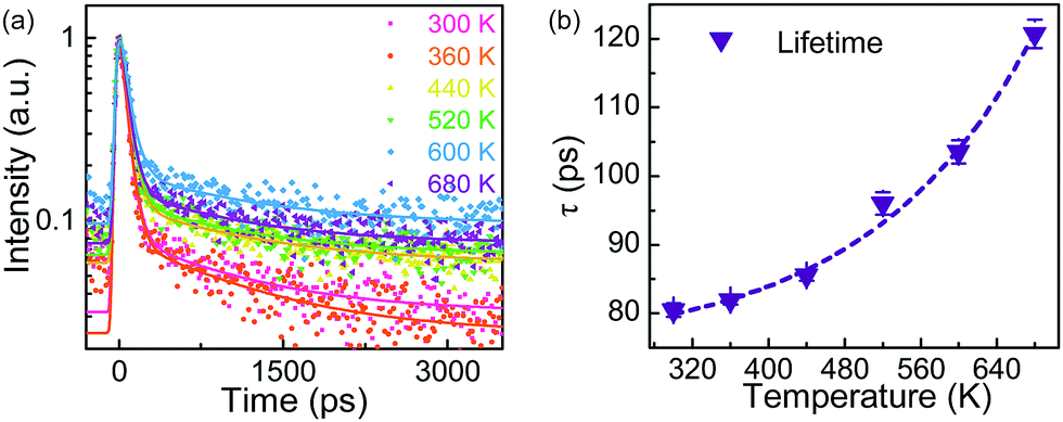 | ||
| Fig. 5 (a) Time-resolved PL spectra of the K → K direct emission at different temperatures. The solid lines are exponential decay fittings of the obtained experimental data points, giving out the effective fluorescence lifetime of the K → K direct emission. (b) The fitted effective lifetime τ as a function of the measurement temperature. | ||
One may argue that the thermal expansion induced interlayer decoupling effect can switch the band-gap structure of ML-WS2 from indirect transition to direct transition, and thus improve its PL intensity.27 However, such a scenario cannot happen in the current case because of the extremely small thermal expansion coefficient of the ML-WS2 sample. The estimated increment in the c-axis interlayer distance (Δd) is ∼0.005 Å at 760 K, which is far less than the necessary Δd of ∼0.97 Å for the occurrence of indirect-to-direct band-gap switching in ML-WS2. As for the in-plane a-axis thermal expansion, its Δd is also very small (∼0.009 Å) and has almost no impact on the band-gap structure of ML-WS2. Detailed calculations and analyses of the thermal expansion induced band-gap structure evolution in ML-WS2 have been shown in Fig. S2–S4 and Note 4 of the ESI.† In addition, the bandgap structure evolution of ML-WS2 with different layer numbers has also been calculated and discussed in Fig. S5 of the ESI.† On the basis of the above discussion, it is concluded that the thermal expansion induced interlayer decoupling cannot be the main cause responsible for the high-temperature fluorescence enhancement observed in ML-WS2.
Another plausible explanation for the high-temperature induced PL improvement is the formation of more defects (e.g. sulfur vacancies) after the thermal annealing process.39 To rule out this factor, PL and Raman spectra of this ML-WS2 sample are measured before and after the TD-PL test (see Fig. S6 of the ESI†). As can be seen, the PL and Raman spectra before/after the TD-PL test look almost the same. No obvious peak broadening or wavelength shift occurs, suggesting that there is no notable defect multiplication after the TD-PL test. Therefore, the observed PL variation is not induced by the formation of more defects. In addition, the thickness of the ML-WS2 flake before/after the TD-PL test is nearly unchanged (see Fig. S7 of the ESI†), indicating that the PL enhancement is not improved by the sample thickness change either. Finally, the effects of different supporting substrates and laser excitation power on the PL behavior of ML-WS2 are also studied and discussed in detail (see Fig. S8 and S9 of the ESI†). It is found that the substrate effect (e.g. interfacial strain, lattice mismatch or charge transfer between the substrate and the sample) or laser effect (e.g. power fluctuation, local heating or sample damage) is not the main cause for the observed fluorescence emission enhancement at high temperatures.
Experimental section
ML-WS2 flakes were mechanically exfoliated from a WS2 bulk crystal (SPI Supplies Inc.), and then transferred onto commercially available SiO2/Si substrates (the SiO2 layer is ∼300 nm) for subsequent research. AFM (Bruker Dimension® Icon™) was employed to study the surface topography and sample thickness of these ML-WS2 flakes. A JY HR-800 LabRam Infinity Spectrophotometer, equipped with a 488 nm laser as the excitation source and a Si photodiode as the signal detector, was employed to measure the steady-state PL and Raman spectra. The laser output power is fixed at ∼1 mW during the temperature-dependent PL measurements, and the laser spot size is focused to be ∼0.5 μm. Thus, the laser power density is ∼4 mW μm−2. A time-correlated single-photon counting technique (TCSPC, B&H Company) was used to record the time-resolved PL spectra of the ML-WS2 samples. The corresponding excitation light source for the TR-PL test is a 530 nm laser generated from a Mira 900 oscillator pulsed laser source with a repetition rate of 76 MHz and a pulse width of 120 fs. An electric heater (Linkam, TMS 600), equipped with an argon gas blower (preventing the samples from being oxidized at high temperatures), was adopted to heat the ML-WS2 flakes for temperature-dependent PL (including steady-state and transient-state) and Raman characterization.Conclusions
In summary, a hot-carrier dynamic model is established based on the high-temperature driven inter-valley transfer mechanism of excited-state carriers among different energy valleys and hills. Significant fluorescence emission enhancement deduced from this model is indeed observed in the ML-WS2 nanoflake for the first time. Population ratio calculations and multiple spectral characterization techniques (including TD-PL and TR-PL) confirm the validity and reliability of this established inter-valley transfer model. The present study not only suggests an efficient strategy to enhance the luminescence performance of indirect-band-gap ML-TMDs, but also sheds more light on the carrier dynamic mechanism (e.g. transfer, relaxation, scattering, and recombination) of 2D materials, both of which are very important to develop new-type electronic and photonic devices based on these emerging materials.Conflicts of interest
There are no conflicts to declare.Acknowledgements
This work was supported by the NSFC for Excellent Young Scholars (No. 51422201), the NSFC Program (No. 61505026, 51732003, 61574031, 51372035, 61604037, 61774031, 51701037 and 21501167), the “111” Project (No. B13013), the Fund from Jilin Province (No. 20160101324JC, 20160520009JH, 20160520115JH and JJKH20180007KJ), the fund by Postdoctoral Science Foundation (No. 2017M621189) and the Fundamental Research Funds for the Central Universities (No. 2412017FZ010).References
- W. Choi, N. Choudhary, G. H. Han, J. Park, D. Akinwande and Y. H. Lee, Mater. Today, 2017, 20, 116–130 CrossRef.
- S. Manzeli, D. Ovchinnikov, D. Pasquier, O. V. Yazyev and A. Kis, Nat. Rev. Mater., 2017, 2, 17033 CrossRef.
- Q. H. Wang, K. Kalantar-Zadeh, A. Kis, J. N. Coleman and M. S. Strano, Nat. Nanotechnol., 2012, 7, 699–712 CrossRef PubMed.
- H. Li, J. Wu, Z. Yin and H. Zhang, Acc. Chem. Res., 2014, 47, 1067–1075 CrossRef PubMed.
- K. M. McCreary, A. T. Hanbicki, G. G. Jernigan, J. C. Culbertson and B. T. Jonker, Sci. Rep., 2016, 6, 19159 CrossRef PubMed.
- M. Samadi, N. Sarikhani, M. Zirak, H. Zhang, H. Zhang and A. Z. Moshfegh, Nanoscale Horiz., 2018, 3, 90–204 RSC.
- M. L. Tsai, M. Y. Li, Y. Shi, L. J. Chen, L. J. Li and J. H. He, Nanoscale Horiz., 2017, 2, 37–42 RSC.
- M. Z. Bellus, M. Li, S. Lane, F. Ceballos, Q. Cui, X. C. Zeng and H. Zhao, Nanoscale Horiz., 2017, 2, 31–36 RSC.
- A. Splendiani, L. Sun, Y. Zhang, T. Li, J. Kim, C.-Y. Chim, G. Galli and F. Wang, Nano Lett., 2010, 10, 1271–1275 CrossRef PubMed.
- J. K. Ellis, M. J. Lucero and G. E. Scuseria, Appl. Phys. Lett., 2011, 99, 261908 CrossRef.
- K. F. Mak, C. Lee, J. Hone, J. Shan and T. F. Heinz, Phys. Rev. Lett., 2010, 105, 136805 CrossRef PubMed.
- M. Chhowalla, H. S. Shin, G. Eda, L.-J. Li, K. P. Loh and H. Zhang, Nat. Chem., 2013, 5, 263–275 CrossRef PubMed.
- R. Dhall, M. R. Neupane, D. Wickramaratne, M. Mecklenburg, Z. Li, C. Moore, R. K. Lake and S. Cronin, Adv. Mater., 2015, 27, 1573–1578 CrossRef PubMed.
- P. Tonndorf, R. Schmidt, P. Böttger, X. Zhang, J. Börner, A. Liebig, M. Albrecht, C. Kloc, O. Gordan, D. R. T. Zahn, S. Michaelis de Vasconcellos and R. Bratschitsch, Opt. Express, 2013, 21, 4908–4916 CrossRef PubMed.
- K. Kośmider and J. Fernández-Rossier, Phys. Rev. B: Condens. Matter Mater. Phys., 2013, 87, 075451 CrossRef.
- Z. Y. Zhu, Y. C. Cheng and U. Schwingenschlögl, Phys. Rev. B: Condens. Matter Mater. Phys., 2011, 84, 153402 CrossRef.
- P. R. Pudasaini, A. Oyedele, C. Zhang, M. G. Stanford, N. Cross, A. T. Wong, A. N. Hoffman, K. Xiao, G. Duscher, D. G. Mandrus, T. Z. Ward and P. D. Rack, Nano Res., 2017, 11, 722–730 CrossRef.
- Y. Wen, Y. Xia and S. Zhang, J. Power Sources, 2016, 307, 593–598 CrossRef.
- S. Jo, N. Ubrig, H. Berger, A. B. Kuzmenko and A. F. Morpurgo, Nano Lett., 2014, 14, 2019–2025 CrossRef PubMed.
- Y. Li, H. Xu, W. Liu, G. Yang, J. Shi, Z. Liu, X. Liu, Z. Wang, Q. Tang and Y. Liu, Small, 2017, 13, 1700157 CrossRef PubMed.
- S. L. Li, K. WaKabayashi, Y. Xu, S. Nakaharai, K. Komatsu, W. W. Li, Y. F. Lin, A. Aparecido-Ferreira and K. Tsukagoshi, Nano Lett., 2013, 13, 3546–3552 CrossRef PubMed.
- S. Kim, A. Konar, W. S. Hwang, J. H. Lee, J. Lee, J. Yang, C. Jung, H. Kim, J. B. Yoo, J. Y. Choi, Y. W. Jin, S. Y. Lee, D. Jena, W. Choi and K. Kim, Nat. Commun., 2012, 3, 1011 CrossRef PubMed.
- T. Cao, G. Wang, W. Han, H. Ye, C. Zhu, J. Shi, Q. Niu, P. Tan, E. Wang, B. Liu and J. Feng, Nat. Commun., 2012, 3, 887 CrossRef PubMed.
- W. Zhao, R. M. Ribeiro, M. Toh, A. Carvalho, C. Kloc, A. H. Castro Neto and G. Eda, Nano Lett., 2013, 13, 5627–5634 CrossRef PubMed.
- D. Li, R. Cheng, H. Zhou, C. Wang, A. Yin, Y. Chen, N. O. Weiss, Y. Huang and X. Duan, Nat. Commun., 2015, 6, 7509 CrossRef PubMed.
- T. Yu and M. W. Wu, Phys. Rev. B: Condens. Matter Mater. Phys., 2014, 90, 035437 CrossRef.
- S. Tongay, J. Zhou, C. Ataca, K. Lo, T. S. Matthews, J. Li, J. C. Grossman and J. Wu, Nano Lett., 2012, 12, 5576–5580 CrossRef PubMed.
- K. P. O’Donnell and X. Chen, Appl. Phys. Lett., 1991, 58, 2924–2926 CrossRef.
- J. S. Ross, S. Wu, H. Yu, N. J. Ghimire, A. M. Jones, G. Aivazian, J. Yan, D. G. Mandrus, D. Xiao, W. Yao and X. Xu, Nat. Commun., 2013, 4, 1474 CrossRef PubMed.
- L. Yuan and L. Huang, Nanoscale, 2015, 7, 7402 RSC.
- G. Froehlicher, E. Lorchat and S. Berciaud, Phys. Rev. B, 2016, 94, 085429 CrossRef.
- Z. Jin, X. Li, J. T. Mullen and K. W. Kim, Physics, 2014, 90, 55–58 Search PubMed.
- P. D. Cunningham, K. M. Mccreary and B. T. Jonker, J. Phys. Chem. Lett., 2016, 7, 5242 CrossRef PubMed.
- A. Colev, C. Gherman, V. Mirovitskii, L. Kulyuk and E. Fortin, J. Lumin., 2009, 129, 1945–1947 CrossRef.
- J. D. Yao, Z. Q. Zheng, J. M. Shao and G. W. Yang, Nanoscale, 2015, 7, 14974–14981 RSC.
- M. Palummo, M. Bernardi and J. C. Grossman, Nano Lett., 2015, 15, 2794 CrossRef PubMed.
- H. Shi, R. Yan, S. Bertolazzi, J. Brivio, B. Gao, A. Kis, D. Jena, H. G. Xing and L. Huang, ACS Nano, 2013, 7, 1072–1080 CrossRef PubMed.
- M. K. Kwon, J. Y. Kim, B. H. Kim, I. K. Park, C. Y. Cho, C. C. Byeon and S. J. Park, Adv. Mater., 2008, 20, 1253–1257 CrossRef.
- S. Tongay, J. Suh, C. Ataca, W. Fan, A. Luce, J. S. Kang, J. Liu, C. Ko, R. Raghunathanan and J. Zhou, Sci. Rep., 2013, 3, 2657 CrossRef PubMed.
Footnote |
| † Electronic supplementary information (ESI) available. See DOI: 10.1039/c8nh00123e |
| This journal is © The Royal Society of Chemistry 2018 |