
 Open Access Article
 This Open Access Article is licensed under a
 Creative Commons Attribution 3.0 Unported Licence
Gradient in defect density of ZnO nanorods grown by cathodic delamination, a corrosion process, leads to end-specific luminescence
Danish
Iqbal
a,
Adnan
Sarfraz
a and
Andreas
Erbe
 *ab
*ab
aMax-Planck-Institut für Eisenforschung GmbH, Max-Planck-Str. 1, 40237 Düsseldorf, Germany. E-mail: defect-density-gradient@the-passivists.org; Fax: +49 211 6792 218; Tel: +49 211 6792 890
bDepartment of Materials Science and Engineering, NTNU, Norwegian University of Science and Technology, 7491 Trondheim, Norway
First published on 20th September 2017
Abstract
ZnO nanorods were grown on a zinc substrate via cathodic delamination of a polymer coating, a tailored corrosion process, at room temperature. A comparison between in situ Raman spectra and post mortem cross sectional analysis by Raman spectroscopy, photoluminescence spectroscopy and scanning electron microscopy shows that in the initial stages of the synthesis, preferentially defect rich ZnO grows. At later stages, crystalline wurtzite ZnO growth dominates. The result is nanorod arrays consisting of nanorods with a large density of point defects in the ≈500 nm range near the zinc substrate, and low defect density in the regions further away from the interface. The growth, which proceeds over several hours, can be interrupted at any time. Large salt concentrations in the corrosive medium increase the growth rate, but also the amount of point defects. The resulting rods show strongly position-dependent luminescence and Raman spectra. Different luminescence can thus be selectively excited, based on the position of excitation.
Conceptual insightsZnO nanorods have been suggested for a number of applications, because of their chemical properties, their optoelectronic properties, and their piezoelectricity. Point defects in the nanorods affect light absorption as well as emission, and catalytic properties. Rods with a low density of defects as well as those with a high density have been used in different applications. This work shows that by using the corrosion process of cathodic delamination of a polymer coating from zinc, rods can be produced with different defect densities at both ends. These “Janus” type rods hence show different luminescence and Raman spectra at both ends. The synthesis can be easily monitored in situ and interrupted to produce rods of different lengths and optical properties. These particles show that the optical and electronic properties can be different in a single particle, produced by a scalable method. |
1 Introduction
ZnO nanostructures have shown interesting optical, mechanical, chemical and electrical properties.1 Applications include their use in electrochemical lithium storage batteries,2 for gas sensing,3 in perovskite solar cells,4,5 or as photocatalysts.6,7 Linking nanostructures together, e.g. in nanotetrapod networks, results in extended application possibilities.8,9 Traditional synthesis methods for ZnO-based nanodevices include chemical vapor deposition (CVD),10 vapor–liquid–solid growth (VLS),11,12 pulsed laser deposition,13 and hydrothermal synthesis.14,15 The hydrothermal approach is interesting due to its simplicity, commercial feasibility, and scalability.16,17 ZnO nanorods on various heterogeneous substrates have been synthesised via solution phase approaches.16 Our group has introduced a simple sequential growth method, via the corrosion process of cathodic delamination, which works completely at room temperature, and yields rods growing in the (0001) direction.18 Cathodic delamination of polymer coatings occurs especially on zinc and steels during exposure to high humidity; a delamination front moves along the metal/polymer interface, with oxygen reduction leading to alkaline conditions at the front, a zone of intermediate pH where corrosion products form in the middle, and a zone of metal dissolution tailing behind.19 Other groups have exploited nanostructural changes during corrosion of zinc nanoparticles.20A key towards designing ZnO nanostructures lies in the detailed understanding of the growth process. Many previous in situ studies of the growth kinetics of ZnO nanostructures were based on UV-Vis spectroscopy.21,22 Laser assisted hydrothermal growth of ZnO nanowires was investigated by optical in situ growth monitoring.23 Transmission X-ray microscopy has been used to detect ZnO nucleation and growth.24 In transmission electron microscopy, cation exchange could be observed in situ.25 Raman spectroscopy as a simple, lab-based, nondestructive technique has been widely used to probe the physical state, phonon confinement, and crystal structure of ZnO.26 Wurzite-type ZnO as the most common ZnO modification belongs to the P63mc space group, where all atoms occupy C3u sites. According to group theory, four Raman active modes of symmetries A1, E1, and E2 (high and low) are expected for wurtzite ZnO. The phonons belonging to A1 and E1 symmetry are polar and therefore exhibit different transverse-optical (TO) and longitudinal-optical (LO) frequencies.27 On the other hand, E2 modes are due to the vibration of the Zn sub-lattice (E2-low) or O sublattice (E2-high).27 Consequently, Raman spectroscopy was utilized to determine the crystal orientation of anisotropic ZnO nanorods.1 Moreover, it has been employed for in situ analysis of electronic and structural aspects of passive ZnO films grown under alkaline conditions.28 Defects change the activity of certain modes,29,30 and lead to photoluminescence. The latter has also been exploited for rapid characterisation of defects in ZnO.31 Raman-inactive modes may for defect-free materials also be probed by hyper-Raman scattering.32
Point defects affect the electronic structure and hence the optical properties, which has been exploited e.g. for white light emitters,33–35 in photocatalysis,18,36 or in whispering gallery mode sensors.37 Thermal annealing reduces the defect density.35,38 Likewise, decoration with carbon-based materials was used to heal defects.39 Doping as an intended introduction of defects is suitable to tune the band structure of ZnO based materials,40 which was used, e.g. in self-powered photodetection.41 For all synthesized ZnO nanostructures, there is a trade-off between conductivity and near band edge emission efficiency. High conductivity in ZnO is achieved by increasing the number of defects in ZnO to provide sufficient free carriers. However, this comes with a compromise in near band edge emission efficiency due to direct interband radiative recombination.42 In visible light photocatalysis, it is crucial to ensure sufficient light absorption in the visible region, for which several strategies exist.7,18,36 There is overall still room for exploiting the role of defects in reliability and performance of devices for a number of applications.43
Recent developments include modifications of the nanostructure's properties, or exploiting local differences within the nanostructures. For instance, local differences in luminescence emission have been achieved,44,45 especially “fluorescence intensification on nanorod ends”.46 Raman scattering was also observed to be spatially distinct, and modulated by polarisation.47 Strain gradients have been used to modulate the exciton emission on ZnO nanowires.48
The aim of this study is to help tailor the local defect structure of ZnO nanorod arrays, by in situ monitoring of the growth processes. Therefore, the growth of ZnO nanorod arrays on metallic zinc during a cathodic delamination corrosion process has been investigated by in situ and operando Raman and photoluminescence (PL) spectroscopy. At specific times, cross sections through the ZnO rods have been prepared and spectra from line scans have been placed in relation to the surface morphology obtained by scanning electron microscopy (SEM).
2 Experimental details
2.1 Materials
Poly(vinyl butyral) [PVB], absolute ethanol and KCl were obtained from Sigma Aldrich and used as received. Zinc sheets (purity 99.95%) having a thickness of 1.5 mm were obtained from Goodfellow (Cambridge, UK). Zinc sheets (1 cm × 1 cm × 1.5 mm) were initially mechanically prepared using 4000 grit polishing paper and then cleaned ultrasonically in ethanol.2.2 Formation of ZnO nanostructures during in situ Raman experiments
The preparation follows the procedure described previously.18 Zinc sheets were spin coated with a 5 wt% solution of PVB in ethanol, followed by drying at 70 °C, to obtain a ≈2 μm thick polymer layer. Afterwards, a small defect was created in the polymer coating ≈1 mm from the edge of the sample. Subsequently, the sample was placed on a zinc base plate. Then, a small reservoir was built around the edge of the sample with the help of a fast drying two components adhesive, which was used to place an electrolyte. To start the cathodic delamination process with growth of ZnO nanowires, the electrolyte reservoir was filled with 1 M or 3 M aqueous KCl.To carry out in situ Raman measurements, the assembly of the sample mounted on the zinc plate was introduced into a custom made chamber with a glass window on top. To minimize electrolyte evaporation, the relative humidity was controlled at ≥90% via the flow of humid and dry air that were mixed in an appropriate ratio. The in situ Raman spectra were recorded using a Horiba Jobin Yvon LabRAM confocal Raman microscope with a Ar+ laser source (emission wavelength 514 nm/2.41 eV) at an output power of 12 mW. The typical spectral acquisition time was in the range of 20–30 s. The measurements were performed in backscattering geometry with a 50× long working distance objective (numerical aperture 0.5) for sample illumination and collection of backscattered light. The laser spot size on the sample surface was approximately 10 μm. The spectrum in which ZnO and H2O peaks were detected for the first time was used as growth time 0, i.e. the first spectrum for analysis. The growth kinetics was monitored at one measurement spot with time.
After the completion of ZnO nanowire growth, the PVB coating was removed by washing with ethanol, followed by rinsing with distilled water to remove any traces of remaining KCl. The washed samples were dried in a nitrogen stream and stored under vacuum for further analysis. Storage times were minimised by conducting analyses as quickly as possible after preparation.
2.3 Post-mortem analysis
Ex situ Raman measurements of cross sections were performed using a Witec alpha300M confocal Raman microscope, with a frequency doubled Nd:YAG laser source (emission wavelength: 532 nm/2.33 eV). Measurements were performed through a microscope objective of 100×, numerical aperture 0.75, in backscattering geometry. For photoluminescence (PL) experiments, a UV laser source (emission wavelength: 355 nm/3.49 eV) was used at the same setup.Sample surface morphology was investigated by scanning electron microscopy (SEM, Zeiss/LEO 1550 VP). In analyses correlating Raman spectra and SEM, the correlating measurements were always conducted immediately one after the other, to avoid significant changes in the samples during storage.
Reflectance absorbance UV/Vis spectra were recorded on an external reflection setup on a Perkin Elmer Lambda 900 spectrometer.
3 Results and discussion
3.1 Monitoring of nanorod growth in 1 M KCl
Fig. 1 shows the measured Raman spectra from a delaminating sample as a function of time. At the initial stages of the experiment, hardly any discernible peaks were observed. As the electrolyte in the delamination front approaches the measurement spot, the band at ≈565 cm−1 begins to evolve (see Fig. 1a). This peak is attributed to the A1-LO phonon mode of ZnO, indicating the growth of strongly disordered ZnO.29,30 Corrosion product growth is caused by degradation of the metal/polymer interface, accompanied by pH changes in the vicinity of the delamination front caused by oxygen reduction.49–52 Zn(OH)2 is believed to be a precursor that forms during corrosion of zinc and which eventually transforms to ZnO.51 However, no evidence of the presence of Zn(OH)2 within the sensitivity level of these in situ Raman measurements could be found, in agreement with previous studies performed on zinc corrosion under alkaline conditions.28,53 After the initial growth phase, one additional band evolves at ≈440 cm−1, which also grows with time. This peak is assigned to the high E2 phonon mode of crystalline wurtzite ZnO,54 indicating the growth of such crystals. After 12 h, no further increase in the peak intensities has been observed, which indicates that the growth of ZnO at a significant rate was terminated.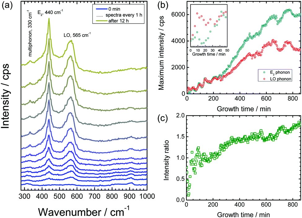 | ||
| Fig. 1 Raman spectra recorded in situ and operando during growth of ZnO nanorods with 1 M KCl. (a) Raman spectra (cps – counts per second) as a function of time. The spectra have been vertically offset for clarity. (b) Intensities of peak maxima of the E2 peak at 440 cm−1 and the LO phonon peak at 570 cm−1 after subtraction of a constant intensity offset as a baseline. Inset: Intensities during the initial phase of oxide growth. (c) Intensity ratio of the E2 peak to LO peak as a function of time. | ||
The increase in peak height of the ZnO E2 mode (440 cm−1) and LO phonon (565 cm−1) as a function of time is depicted in Fig. 1b. Both intensities increase, and it is obvious from the plot that initially, the LO phonon is the dominant peak, while at longer growth times, the E2 mode is the mode detected with highest intensity. The ratio of the maximum intensity of the E2 peak (440 cm−1) to the LO peak (565 cm−1) as a function of time is plotted in Fig. 1c. In the initial stages of oxide growth, this peak height ratio is <1, indicating growth of predominantly defect-rich ZnO. However, after ≈2 h, the growth of crystalline wurtzite ZnO dominates. Finally, after ≈12 h, the ratio remains stable, indicating that no further changes in the crystal structure and defect density of growing ZnO take place.
Two scenarios can lead to the observed Raman spectra: (a) the initially growing oxide is defect rich and crystallises in the course of the growth process, or (b) on top of the intial defect rich oxide, a defect poor oxide grows at later stages, with growth in the radial as well as longitudinal direction as possibilities. To investigate if (a) or (b) is observed in practice, cross sections of the samples were analysed (Fig. 2). The SEM images (Fig. 2a) confirm that width and length are as previously reported,18 20–70 nm and 800–1000 nm, respectively. Fig. 2 also shows the Raman and PL spectra measured along a cross section through the nanorods with excitation at 532 nm/2.33 eV and 355 nm/3.49 eV. For better visualization of differences in the peak intensities along the length of the rod, different colours were used to plot the spectra. Fig. 2e shows the room temperature PL spectra at selected points along a cross section through the ZnO nanorod layer as indicated in the SEM image shown in Fig. 2a. It is evident from the PL spectra that the intensity of the green emission centred around 2.5 eV, and which is related to the presence of oxygen vacancies or other oxygen-related point defects,30,34,55 is different along the growth direction of the nanorod layer. The full evolution of the spectra along the growth direction in Fig. 2f show strong defect related luminescence at the bottom of the layer near the Zn substrate. The intensity of the defect related luminescence decreases until the top of the layer, whereas the intensity of the main excitonic transition at 3.3 eV remains almost constant along the layer. These observations indicate a low defect density,56 and good crystallinity, at the top of the layer.57 On the other hand, the higher green emission intensity at the bottom of the rod indicates a higher density of oxygen-related defects.
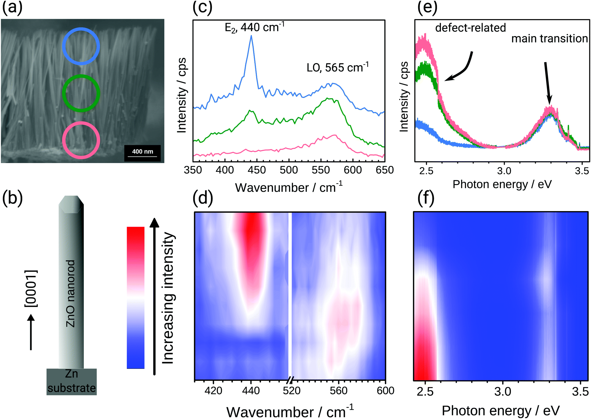 | ||
| Fig. 2 (a) SEM image of a cross section through a fully grown nanorod array. The circles with different colours show the regions in which the spectra displayed in (c) and (e) were recorded. (b) Schematic drawing of a ZnO nanorod to show the direction in which spectral line scans displayed in (d) and (f) were recorded. (c) Raman spectra from selected positions and (d) Raman line scan parallel to the growth direction of the nanorods recorded with excitation at 532 nm/2.33 eV. (e) PL spectra from selected positions and (d) PL line scan recorded parallel to the growth direction of the nanorods with excitation at 355 nm/3.49 eV. Colours used in spectra (c) and (e) are used to encode the position marked with circles in (a) coloured in red, green and blue, corresponding to the lower region, middle region and upper region of the nanorod layer, respectively. The Raman (d) and PL (f) line scans use a false colour encoding to display the spectral evolution along the growth direction of the rods as indicated in (b): blue – low intensity, red – high intensity. All measurements, SEM, Raman and PL shown here were recorded subsequently on the same sample, leading to compromises in image quality. | ||
Similarly, Raman measurements were performed along the length of a ZnO nanorod layer, as shown in Fig. 2c and d, respectively, with excitation at a photon energy below the band gap, at 532 nm/2.33 eV. The ZnO spectra overall are dominated by two main bands centred around 440 cm−1 (E2-high) and 565 cm−1 (E1-LO).54 Both bands change in intensity along the cross section. At the bottom of the nanorod layer (red circle region), the intensity of the E1 band is high, and the E2 band is barely visible. Such a spectrum is an indication of an extremely defect-rich ZnO.29,30 In the upper region of the nanorod layer (blue circle) the intensity of the E1 band gets lower, and the E2 band is dominating, indicating the presence of more crystalline ZnO. In the centre region, marked with a green circle, both crystalline and defect rich ZnO are present. A detailed discussion of the Raman spectra of ZnO grown under electrochemical polarisation is available elsewhere.30
Overall, both ex situ Raman and PL analyses along a cross section of the nanorod corrosion product layer show that the bottom region is defect-rich (Fig. 2). In situ, the initially grown region, i.e. the bottom region, is also defect rich (Fig. 1). The comparison with the ex situ data shows that the increasing crystallinity observed in situ is not because of a remodelling of the surface, but rather because of the continued growth of structures which are highly crystalline.
It is an interesting question if other growth methods of substrate-bound ZnO nanorod arrays, such as the hydrothermal method, would also lead to changes in the defect structure along the growth direction of rods. In the case of substrate-free growth of nanostructures nucleating from solution, no gradient in defect structure would be expected. On a substrate, lattice strain must lead to changes in the crystal lattice in immediate contact with the substrate, however, not necessarily on a mesoscopic scale along the growing rod. We attribute the occurrence of a defect density gradient in connection with the growth by cathodic delamination to a specific change in growth environment, caused by the progress of the delamination process and the corresponding change in pH and environmental composition, at the same time as the growth progresses. Oscillations, with redissolution of initially formed oxide,52 also contributes to the development of the defect density gradient. In this manner, all rods at a certain position after the passage of the delamination front experience quite similar conditions. The change in pH accompanied by the passage of the delamination front will determine the growth conditions, and consequently the resulting nanorod properties. If a similar change in conditions occurs also in other growth techniques, a similar variation in defect density is to be expected.
3.2 Evolution of surface morphology during growth
To gain further insight into the growth of the ZnO nanorods, SEM micrographs with their corresponding Raman spectra were obtained after specific time intervals of corrosion product growth (Fig. 3). During the initial stages of growth, the zinc surface is covered with a thin, disordered oxide layer [Fig. 3(IA)]. The Raman spectrum [Fig. 3(IC)] is typical for ZnO without long-range crystalline order. After ≈1 h, short nanorod structures of ZnO are already visible [Fig. 3(IIA and B)]. These show the presence with low intensity of the wurtzite E2 mode at 440 cm−1. Finally, after 12 h, the ZnO nanorods are grown up to 1 μm [Fig. 3(IIIA and B)] and the wurtzite E2 mode at 440 cm−1 is dominating in the corresponding Raman spectra. The comparison of the peak heights of the bands at 440 and 570 cm−1 with the SEM images suggests that the band typical for crystalline ZnO becomes dominant only after the crystalline rod-like structures are formed. On the other hand, the corrosion products formed in the initial stage show spectra with a dominating LO phonon at 570 cm−1, which is typical for strongly disordered and defective ZnO. As observed during in situ experiments (Fig. 1), the intensity of the mode at 570 cm−1 grows slower than the mode at 440 cm−1. This observation also suggests that the fraction of defects forming during growth of the ZnO crystals reduces as the growth progresses.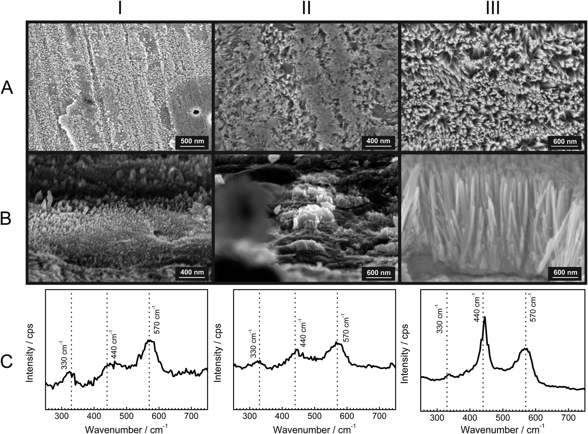 | ||
| Fig. 3 Time evolution of growing ZnO nanorods (1 M KCl). Columns: I – after 15 min, II – after 1 h, III – after 12 h. Rows: A – SEM top view, B – SEM cross-sectional view, C – ex situ Raman spectra. In the Raman spectra, the wavenumbers of typical ZnO modes, 330 cm−1, 440 cm−1, and 570 cm−1 are marked with dashed lines. Data in each column were recorded subsequently on the same sample. | ||
A comparison of the structures along row A in Fig. 3 shows that the diameter of the rods increases at best marginally during the growth stage where the rods grow in length. Consequently, radial growth cannot be the main reason for the observed significant differences in the Raman spectra along row C in Fig. 3. The dominance of crystalline wurzite ZnO in the Raman spectra clearly correlates with the growth in length.
3.3 Effect of electrolyte concentration on the resulting structures
Previous studies have shown that corrosion of zinc is accelerated by increase in the concentration of Cl− ions in aqueous solutions.58,59 Hence, the effect was investigated of chloride concentration on the growth kinetics and defect density of the obtained ZnO nanorods. For this purpose, the same experiments as mentioned above have been conducted also with 3 M KCl as delamination electrolyte. Fig. 4a depicts the measured Raman spectra from a delaminating zinc sample as a function of time. As in the case of 1 M KCl, initially the ZnO LO phonon appears, which corresponds to growth of defect rich ZnO. Later on, the wurtzite E2 peak grows with time (Fig. 4b). The increase in intensity of the E2 band stops after ≈4 h. This observation suggests that no further ZnO growth takes place. The intensity ratio E2/LO (Fig. 4c) for the initial ≈30 min is <1, which is an indication that growth of defect rich ZnO is dominating over the growth of wurtzite ZnO. As observed for 1 M KCl, and already discussed elsewhere,52 oscillations in intensity are observed in the initial phase of the experiment. The trends for growth of ZnO nanorods in both 1 M KCl and 3 M KCl are similar, however the overall growth rate is higher in 3 M KCl. The slightly higher intensities of the ZnO peak suggest the presence of a higher number of defects in the faster grown rods from a 3 M KCl delamination electrolyte. The time evolution of morphology and the corresponding Raman spectra were also monitored in 3 M KCl (Fig. 5). The results depict similar conclusions drawn before: initially strongly disordered/amorphous ZnO grows, while in later stages, the growth of crystalline ZnO becomes pronounced. | ||
| Fig. 4 Raman spectra recorded in situ and operando during growth of ZnO nanorods with 3 M KCl. (a) Raman spectra as a function of time. The spectra have been vertically offset for clarity. (b) Intensities of peak maxima of the E2 peak at 440 cm−1 and the LO phonon peak at 570 cm−1 after subtraction of a constant intensity offset as the baseline. Inset: Intensities during the initial phase of oxide growth. (c) Intensity ratio of the E2 peak to LO peak as a function of time. | ||
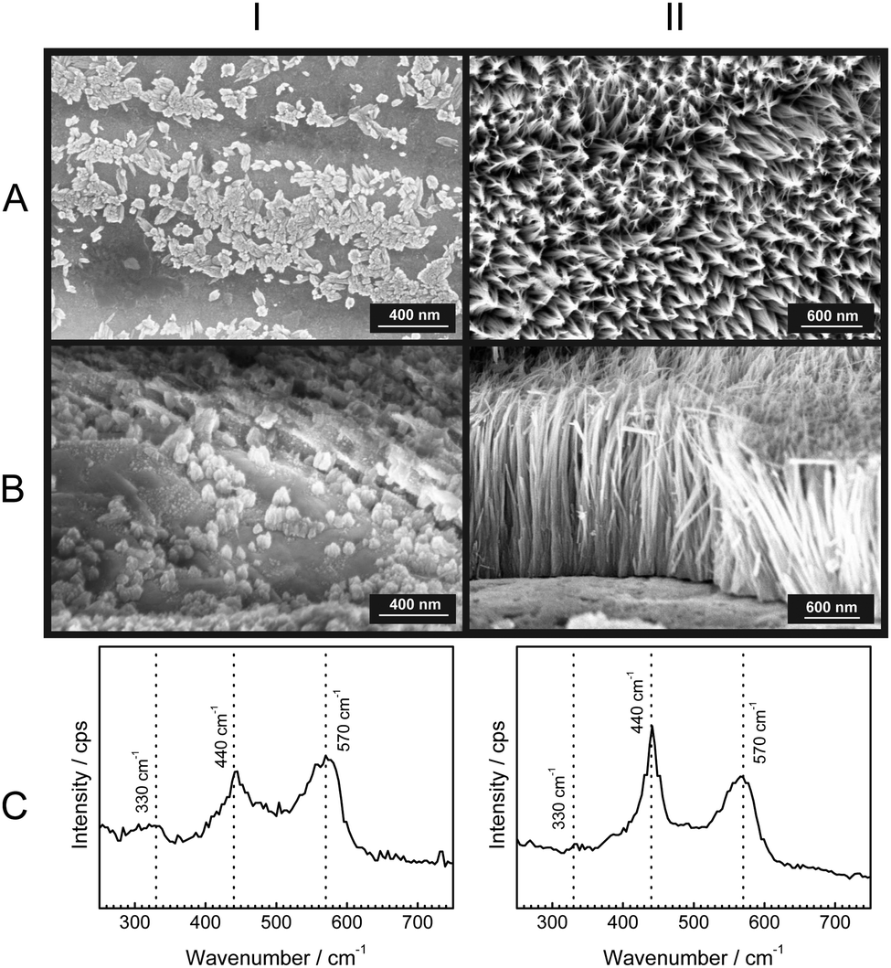 | ||
| Fig. 5 Time evolution of growing ZnO nanorods (3 M KCl). Columns: I – after 15 min, II – after 4.5 h. Rows: A – SEM top view, B – SEM cross-sectional view, C – ex situ Raman spectra. In the Raman spectra, the wavenumbers of typical ZnO modes, 330 cm−1, 440 cm−1, and 570 cm−1, are marked with dashed lines. Data in each column was recorded subsequently on the same sample. | ||
3.4 Optical properties of ZnO nanorods
The optical properties of ZnO nanostructures strongly depend on the presence of defects in the crystal. PL spectra are already shown in Fig. 2. To complement these spectra, UV/VIS reflection absorption spectra of the as grown ZnO nanostructures with 1 M and 3 M KCl as a delamination electrolyte are shown in Fig. 6. The spectra show total absorption below ≈370 nm, which corresponds to the main electronic transition from the valence band to the conduction band. Light absorption in the visible region is also strong, attributed to a combination of absorption and scattering processes. Absorbance is slightly higher for wires synthesized with 3 M KCl. The higher absorbance can be explained by the larger concentration of defects in the nanorods grown in 3 M KCl.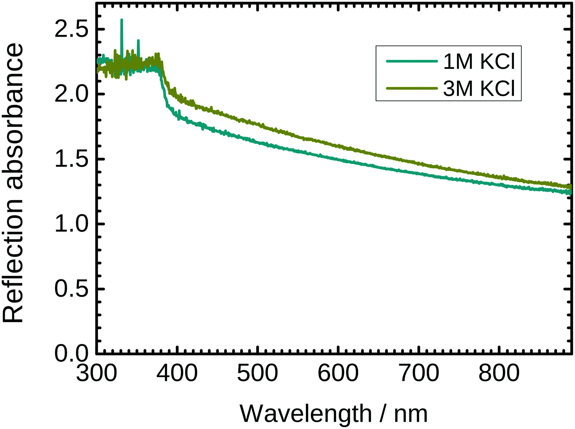 | ||
| Fig. 6 UV/VIS reflection absorption spectrum of ZnO nanorod arrays grown with 1 M KCl and 3 M KCl as a delamination electrolyte, respectively. A clean zinc sheet was used as a reference in these measurements. | ||
4 Summary and conclusions
Comparing in situ Raman and PL spectra obtained during cathodic delamination with those recorded from cross sections prepared after the growth of ZnO nanorods was terminated shows that at the initial stages of growth, nucleation of defect rich ZnO takes place, while in the later stages growth of wurtzite ZnO becomes pronounced. Well-aligned nanorods form in the later stages of growth. Faster growth at higher electrolyte concentration yields nanorods with more defects. The growth of nanorods stops due to depletion in the concentration of dissolved zinc species. The growth of the nanorods can also be interrupted at any time. The final rods show visible light photoluminescence, with the emission spectrum strongly dependent on the position along the long axis of the nanorods. Such a position dependent change of the emission spectrum in individual nanorods enables interesting perspectives in optoelectronic applications.Conflicts of interest
There are no conflicts of interest to declare.Acknowledgements
D. I. acknowledges a scholarship from the IMPRS Surmat and A. S. funding from Maxnet Energy. Prof. M. Stratmann is acknowledged for continuous support, and P. Ebbinghaus for technical assistance. Open Access funding provided by the Max Planck Society.References
- S. Singamaneni, M. Gupta, R. Yang, M. M. Tomczak, R. R. Naik, Z. L. Wang and V. V. Tsukruk, ACS Nano, 2009, 3, 2593–2600 CrossRef CAS PubMed.
- J. Zhang, P. Gu, J. Xu, H. Xue and H. Pang, Nanoscale, 2016, 8, 18578–18595 RSC.
- D. R. Miller, S. A. Akbar and P. A. Morris, Sens. Actuators, B, 2014, 204, 250–272 CrossRef CAS.
- S. Li, P. Zhang, Y. Wang, H. Sarvari, D. Liu, J. Wu, Y. Yang, Z. Wang and Z. D. Chen, Nano Res., 2017, 10, 1092–1103 CrossRef CAS.
- S. Li, P. Zhang, H. Chen, Y. Wang, D. Liu, J. Wu, H. Sarvari and Z. D. Chen, J. Power Sources, 2017, 342, 990–997 CrossRef CAS.
- X. Lang, X. Chen and J. Zhao, Chem. Soc. Rev., 2014, 43, 473–486 RSC.
- S. G. Kumar and K. S. R. K. Rao, RSC Adv., 2015, 5, 3306–3351 RSC.
- D. Gedamu, I. Paulowicz, S. Kaps, O. Lupan, S. Wille, G. Haidarschin, Y. K. Mishra and R. Adelung, Adv. Mater., 2014, 26, 1541–1550 CrossRef CAS PubMed.
- Y. K. Mishra, G. Modi, V. Cretu, V. Postica, O. Lupan, T. Reimer, I. Paulowicz, V. Hrkac, W. Benecke, L. Kienle and R. Adelung, ACS Appl. Mater. Interfaces, 2015, 7, 14303–14316 CAS.
- J.-J. Wu and S.-C. Liu, J. Phys. Chem. B, 2002, 106, 9546–9551 CrossRef CAS.
- A. M. Morales and C. M. Lieber, Science, 1998, 279, 208–211 CrossRef CAS PubMed.
- M. H. Huang, Y. Y. Wu, H. Feick, N. Tran, E. Weber and P. D. Yang, Adv. Mater., 2001, 13, 113–116 CrossRef CAS.
- J. H. Choi, H. Tabata and T. Kawai, J. Cryst. Growth, 2001, 226, 493–500 CrossRef CAS.
- H. Yu, Z. Zhang, M. Han, X. Hao and F. Zhu, J. Am. Chem. Soc., 2005, 127, 2378–2379 CrossRef CAS PubMed.
- L. Wang, D. Tsan, B. Stoeber and K. Walus, Adv. Mater., 2012, 24, 3999–4004 CrossRef CAS PubMed.
- L. Vayssieres, Adv. Mater., 2003, 15, 464–466 CrossRef CAS.
- J. Yeo, S. Hong, M. Wanit, H. W. Kang, D. Lee, C. P. Grigoropoulos, H. J. Sung and S. H. Ko, Adv. Funct. Mater., 2013, 23, 3316–3323 CrossRef CAS.
- D. Iqbal, A. Kostka, A. Bashir, A. Sarfraz, Y. Chen, A. D. Wieck and A. Erbe, ACS Appl. Mater. Interfaces, 2014, 6, 18728–18734 CAS.
- C. D. Fernández-Solis, A. Vimalanandan, A. Altin, J. S. Mondragón-Ochoa, K. Kreth, P. Keil and A. Erbe, Fundamentals of Electrochemistry, Corrosion and Corrosion Protection, in Lecture Notes in Physics, ed. R. P. Lang and Y. Liu, Springer, Cham, Switzerland, 2016, ch. 2, vol. 917, pp. 29–70 Search PubMed.
- S. Calderon V., B. Gomes, P. J. Ferreira and S. Carvalho, Nanoscale, 2017, 9, 5254–5262 RSC.
- R. Viswanatha, P. K. Santra, C. Dasgupta and D. D. Sarma, Phys. Rev. Lett., 2007, 98, 255501 CrossRef PubMed.
- E. M. Wong, J. E. Bonevich and P. C. Searson, J. Phys. Chem. B, 1998, 102, 7770–7775 CrossRef CAS.
- J. In, S.-G. Ryu, D. Lee, S. Ahn, A. C. Zheng, D. J.-S. Hwang and C. P. Grigoropoulos, Proc. SPIE, 2013, 8826, 88260E CrossRef.
- S. E. R. Tay, A. E. Goode, J. Nelson Weker, A. A. Cruickshank, S. Heutz, A. E. Porter, M. P. Ryan and M. F. Toney, Nanoscale, 2016, 8, 1849–1853 RSC.
- Y. H. Chen, C. W. Huang, P. H. Yeh, J. Y. Chen, T. Y. Lin, C. F. Chang and W. W. Wu, Nanoscale, 2016, 8, 17039–17043 RSC.
- R. Kattumenu, C. H. Lee, V. N. Bliznyuk and S. Singamaneni, in Raman Spectroscopy for Nanomaterials Characterization, ed. C. S. S. R. Kumar, Springer Berlin Heidelberg, 2012, pp. 417–444 Search PubMed.
- A. C. Gandhi, H.-J. Hung, P.-H. Shih, C.-L. Cheng, Y.-R. Ma and S. Y. Wu, Nanoscale Res. Lett., 2010, 5, 581–586 CrossRef CAS PubMed.
- W. B. Cai and D. A. Scherson, J. Electrochem. Soc., 2003, 150, B217–B223 CrossRef CAS.
- Y. Y. Tay, T. T. Tan, M. H. Liang, F. Boey and S. Li, Appl. Phys. Lett., 2008, 93, 111903 CrossRef.
- Y. Chen, P. Schneider, B.-J. Liu, S. Borodin, B. Ren and A. Erbe, Phys. Chem. Chem. Phys., 2013, 15, 9812–9822 RSC.
- S. Ghosh, M. Ghosh, M. Seibt and G. Mohan Rao, Nanoscale, 2016, 8, 2632–2638 RSC.
- J. Zeng, L. Chen, Q. Dai, S. Lan and S. Tie, Nanoscale, 2016, 8, 1572–1579 RSC.
- X. Zhao, W. Liu, R. Chen, Y. Gao, B. Zhu, H. V. Demir, S. Wang and H. Sun, Nanoscale, 2016, 8, 5835–5841 RSC.
- M. Willander, O. Nur, N. Bano and K. Sultana, New J. Phys., 2009, 11, 125020 CrossRef.
- E. G. Barbagiovanni, R. Reitano, G. Franzo, V. Strano, A. Terrasi and S. Mirabella, Nanoscale, 2016, 8, 995–1006 RSC.
- X. Zhang, J. Qin, Y. Xue, P. Yu, B. Zhang, L. Wang and R. Liu, Sci. Rep., 2014, 4, 04596 CrossRef PubMed.
- R. S. Moirangthem and A. Erbe, Appl. Phys. Lett., 2013, 103, 051108 CrossRef.
- Z.-W. Wu, S.-L. Tyan, H.-H. Chen, J.-C.-A. Huang, C.-L. Wu, C.-R. Lee and T.-S. Mo, RSC Adv., 2017, 7, 5807–5812 RSC.
- C. V. Pham, S. Repp, R. Thomann, M. Krueger, S. Weber and E. Erdem, Nanoscale, 2016, 8, 9682–9687 RSC.
- W. Yang, B. Zhang, Q. Zhang, L. Wang, B. Song, Y. Ding and C. P. Wong, RSC Adv., 2017, 7, 11345–11354 RSC.
- B. D. Boruah, S. N. Majji and A. Misra, Nanoscale, 2017, 9, 4536–4543 RSC.
- H. Ding, N. Pan, C. Ma, Y. Wu, J. Li, H. Cai, K. Zhang, G. Zhang, W. Ren, J. Li, Y. Luo, X. Wang and J. G. Hou, Adv. Mater., 2014, 26, 3035–3041 CrossRef CAS PubMed.
- A. B. Djurisic, X. Chen, Y. H. Leung and A. M. C. Ng, J. Mater. Chem., 2012, 22, 6526–6535 RSC.
- W. T. Ruane, K. M. Johansen, K. D. Leedy, D. C. Look, H. von Wenckstern, M. Grundmann, G. C. Farlow and L. J. Brillson, Nanoscale, 2016, 8, 7631–7637 RSC.
- Y. H. Yang, X. T. He, H. M. Dong, J. W. Dong, H. X. Lei, B. J. Li and G. W. Yang, Nanoscale, 2016, 8, 9226–9233 RSC.
- J. Truong, M. Singh, M. Hansen and J.-i. Hahm, Nanoscale, 2017, 9, 8164–8175 RSC.
- M. Hansen, J. Truong, T. Xie and J.-i. Hahm, Nanoscale, 2017, 9, 8470–8480 RSC.
- X.-W. Fu, C.-Z. Li, L. Fang, D.-M. Liu, J. Xu, D.-P. Yu and Z.-M. Liao, ACS Nano, 2016, 10, 11469–11474 CrossRef CAS PubMed.
- W. Fürbeth and M. Stratmann, Corros. Sci., 2001, 43, 207–227 CrossRef.
- W. Fürbeth and M. Stratmann, Corros. Sci., 2001, 43, 229–241 CrossRef.
- X. G. Zhang, Corrosion and electrochemistry of zinc, Plenum Press, New York, 1996 Search PubMed.
- D. Iqbal, A. Sarfraz, M. Stratmann and A. Erbe, Chem. Commun., 2015, 51, 16041–16044 RSC.
- M. Bernard, A. Hugotlegoff and N. Phillips, J. Electrochem. Soc., 1995, 142, 2162–2167 CrossRef CAS.
- T. C. Damen, S. P. S. Porto and B. Tell, Phys. Rev., 1966, 142, 570–574 CrossRef CAS.
- K. Vanheusden, W. L. Warren, C. H. Seager, D. R. Tallant, J. A. Voigt and B. E. Gnade, J. Appl. Phys., 1996, 79, 7983–7990 CrossRef CAS.
- X. Y. Zhang, J. Y. Dai, H. C. Ong, N. Wang, H. L. W. Chan and C. L. Choy, Chem. Phys. Lett., 2004, 393, 17–21 CrossRef CAS.
- Q. Tang, W. J. Zhou, J. M. Shen, W. Zhang, L. F. Kong and Y. T. Qian, Chem. Commun., 2004, 712–713 RSC.
- E. E. Abd El Aal, Corros. Sci., 2000, 42, 1–16 CrossRef.
- T. Hurlen, Acta Chem. Scand., 1962, 16, 1346–1352 CrossRef CAS.
| This journal is © The Royal Society of Chemistry 2018 |