
A two-dimensional CaSi monolayer with quasi-planar pentacoordinate silicon†
Yu
Wang
a,
Man
Qiao
a,
Yafei
Li
 *a and
Zhongfang
Chen
*b
*a and
Zhongfang
Chen
*b
aJiangsu Collaborative Innovation Centre of Biomedical Functional Materials, Jiangsu Key Laboratory of New Power Batteries, School of Chemistry and Materials Science, Nanjing Normal University, Nanjing, 210023, China. E-mail: liyafei@njnu.edu.cn
bDepartment of Chemistry, Institute for Functional Nanomaterials, University of Puerto Rico, Rio Piedras Campus, San Juan, PR 00931, USA. E-mail: zhongfangchen@gmail.com
First published on 22nd January 2018
Abstract
The prediction of new materials with peculiar topological properties is always desirable to achieve new properties and applications. In this work, by means of density functional theory computations, we extend the rule-breaking chemical bonding of planar pentacoordinate silicon (ppSi) into a periodic system: a C2v Ca4Si22− molecular building block containing a ppSi center is identified first, followed by the construction of an infinite CaSi monolayer, which is essentially a two-dimensional (2D) network of the Ca4Si2 motif. The moderate cohesive energy, absence of imaginary phonon modes, and good resistance to high temperature indicate that the CaSi monolayer is a thermodynamically and kinetically stable structure. In particular, a global minimum search reveals that the ppSi-containing CaSi monolayer is the lowest-energy structure in 2D space, indicating its great promise for experimental realization. The CaSi monolayer is a natural semiconductor with an indirect band gap of 0.5 eV, and it has rather strong optical absorption in the visible region of the solar spectrum. More interestingly, the unique atomic configuration endows the CaSi monolayer with an unusually negative Poisson's ratio. The rule-breaking geometric structure together with its exceptional properties makes the CaSi monolayer quite a promising candidate for applications in electronics, optoelectronics, and mechanics.
Conceptual insightsChemical bonding is one of the most basic concepts of chemistry, and many established bonding rules are the foundations for the understanding of the structure and electronic properties of molecules and solids. Therefore, designing new materials with rule-breaking chemical bonding, e.g. planar hypercoordinate motifs, would be of both theoretical and practical importance. Based on multi-scale simulations, we demonstrate that a two-dimensional CaSi monolayer, in which each Si atom binds with five ligands to form a moiety of quasi-planar pentacoordinate silicon, is thermodynamically, dynamically and thermally stable. Our designed CaSi monolayer is the global minimum structure in 2D space; it possesses a moderate band gap and exhibits an unusually negative Poisson's ratio. |
Introduction
Most main-group elements obey some established rules when forming chemical bonds with other elements and themselves. For example, the tetrahedral preference of saturated sp3 carbon (C) in most known molecules and materials has been established as one of the foundations of organic chemistry.1,2 In addition, C also has a vast flexibility to adopt the linear sp or planar sp2 hybridization coupled with the right valence. In 1968 Monkhorst proposed the rule-breaking “planar tetracoordinate carbon” (ptC) by exampling the fictitious planar methane (D4h),3 which is actually not a local minimum structure. Hoffmann et al.4 then suggested that the ptC moiety can be stabilized electronically by using π-acceptor or σ-donor ligands, or mechanically by enforcing ptC arrangements in strained rings or cages. Under this guidance, Collins et al.5 designed the first ptC-containing molecule (1,1-dilithiocyclopropane) by ab initio computations. In 1977, the first experimentally verified ptC molecule was achieved by Cotton and co-workers.6 In 1991, Boldyrev and Schleyer proposed the bonding rules on the basis of electronic and geometrical considerations to guide the design of ptC-containing molecules,7 which significantly promotes the development of planar carbon chemistry.8–11 Encouragingly, some global minimum ptC species, such as CAl4−,12 CAl42−,13 CAl3Si−,14 and their derivatives, have been identified experimentally by gas-phase photoelectron spectroscopy. More excitingly, the existence of planar hypercoordinate carbons with coordination numbers larger than four, such as planar pentacoordinate carbon (ppC)15,16 and hexacoordinate carbon (phC),17,18 have also been explored theoretically. These fantastic new bonding arrangements are of fundamental significance and have important implications in designing new materials.As another group-14 element, silicon (Si) has distinct bonding characters from those of carbon. For instance, Si tends to utilize all three of its 3p orbitals to adopt the tetrahedral sp3 hybridization, whereas the planar hybridization of silicon is rather rare in nature. Extensive studies of planar hypercoordinate carbon have also motivated scientists to explore molecules with planar hypercoordinate silicon, especially considering that the planar tetracoordination is fundamentally easier to realize with silicon than with carbon.19 In 1979 Schleyer et al. predicted theoretically the first molecule containing a planar tetracoordinate silicon (ptSi) center, i.e. orthosilicic acid ester.20 Afterwards, many ptSi-containing molecules were designed computationally, such as tetraazafenestrane21 and Si(CO)4.22 However, none of these molecules have been realized experimentally. The breakthrough occurred in 2000; Boldyrev et al.23 detected the first ptSi-containing molecule SiAl4− by a joint experimental and theoretical study. In 2004, Li et al.24 proposed a scheme to incorporate ptSi, planar pentacoordinate silicon (ppSi) and hexacoordinate silicon (phSi) in C2v-BnE2Si (E = CH, BH, or Si; n = 2–5). Islas et al.25 designed several planar hypercoordinate silicon species by enclosing Si atoms in boron wheels. These studies significantly enriched the family of planar hypercoordinate silicon moieties. However, at present there are few studies focusing on planar hypercoordinate silicon, and global minimum structures with planar hypercoordinate silicon are rather rare.
It is known that the properties of a material are mainly determined by its structure, and the unique geometric structures usually lead to exotic physicochemical properties. Therefore, it is desirable to extend the bonding arrangements of planar hypercoordinate carbon and silicon into periodic solids and nanostructures, which would bring some unique structures and peculiar potentials for a wide range of applications. The past decade has witnessed the rapid development of this field.26–28 In particular, stimulated by the isolation of graphene and two dimensional (2D) inorganic materials, there has been growing interest in the design of 2D materials containing planar hypercoordinate carbon or silicon, e.g. ptC-containing B2C,29 TiC,30 and Al2C monolayers,31,32 ppC-containing Be5C2 monolayers,33 phC-containing Be2C monolayers,34 and ptSi-containing SiC2 monolayers.35 The novel geometric structures endow these 2D materials with many intriguing properties. For example, Wang et al.33 demonstrated that a Be5C2 monolayer is semimetallic and has an unusually negative Poisson's ratio in the in-plane direction; thus it is appealing for specific applications in electronics and mechanics. The 2D Cu2Si monolayer with phSi bonding was theoretically predicted by Yang et al. in 2015,36 and was just synthesized by Feng et al.37 Besides the unique bonding, Cu2Si presents intriguing Dirac nodal line fermions, which open new avenues to realize high-speed low-dissipation devices.37 Nevertheless, to the best of our knowledge, there is no attempt at designing nanostructures with ppSi, which may be due to the difficulty in finding a suitable type of ligand to electronically or mechanically fit the ppSi in periodic systems.
Here, inspired by the bonding pattern of our newly discovered ppSi species Ca4Si22−, we recognize that calcium (Ca) is a promising ligand to construct ppSi-containing solids. Along this line, we computationally designed a new ppSi-featuring 2D material, namely the CaSi monolayer, in which each Si atom binds with four Ca atoms and one Si atom in almost the same plane to form a quasi ppSi moiety. The ppSi-containing CaSi monolayer has good thermodynamic, kinetic, and mechanical stabilities and is the global minimum structure in 2D space. Due to its exotic geometric structure, the CaSi monolayer presents rather attractive electronic, optical, and mechanical properties.
Methods
For Ca4Si22−, geometry optimizations and electronic structure computations were performed at the M06-2X38 level of theory with the cc-PVTZ basis set as implemented in the Gaussian 03 package.39 The M06-2X functional has been demonstrated to be rather satisfactory for systems consisting of main group elements. The validity of the M06-2X functional for the Ca4Si22− cluster and the PBE functional used for slab model computations was verified by comparison with the CCSD(T)40 and other common methods for the Ca4Si22− cluster (Table S1, ESI†). For the CaSi monolayer, DFT computations were performed using the Vienna ab initio simulation package (VASP),41 with exchange–correlation interactions modeled by the Perdew–Burke–Ernzerhof functional.42 Ion–electron interactions were described using the projector-augmented plane wave (PAW) approach.43,44 The Brillouin zone was sampled with 6 × 8 × 1 k-points. The convergence threshold was set as 10−5 eV in energy and 10−2 eV Å−1 in force. The HSE06 hybrid functional45 was adopted for high-accuracy electronic structure computations. The phonon spectrum was computed using the finite displacement method as implemented in the Phonopy code.46The bonding pattern of the CaSi monolayer was analyzed utilizing the Solid State Adaptive Natural Density Partitioning (SSAdNDP) method,47 which is an extension of the AdNDP method to periodic systems and as such was derived from periodic implementation of the Natural Bond Orbital (NBO) analysis. SSAdNDP allows the interpretation of chemical bonding in systems with translational symmetry in terms of classical lone pairs and two-center bonds, as well as multi-center delocalized bonds.
The thermal stability of the CaSi monolayer was assessed utilizing first principles molecular dynamics (FPMD) simulations within the PBE functional as implemented in VASP. The initial configuration with a 3 × 4 supercell was annealed at three temperatures. Each FPMD simulation (NVT ensemble) lasted for 10 ps with a time step of 1.0 fs. Temperature control is fulfilled using the Nosé–Hoover method.48
The global minimum search for the lowest-energy structure of 2D CaSi was conducted using the particle-swarm optimization (PSO) method within the evolutionary scheme as implemented in the CALYPSO code.49 The population size and the number of generations were set to be 30 in all PSO simulations. We did three structural searches with the unit cell of CaSi monolayers containing 4, 8, and 16 atoms, respectively. The structure relaxations during the PSO simulation were performed using the PBE functional as implemented in VASP. All the structures obtained from the CALYPSO search were re-optimized using VASP.
Results and discussion
Ca4Si22−: an inspiring ppSi species for 2D systems
Our design of a 2D infinite ppSi-containing system was initially motivated by the discovery of a ppSi-containing Ca4Si22− minimum (Fig. 1a), which has the singlet ground state, with the lowest vibrational frequency being 34.2 cm−1 at the M06-2X/cc-pVTZ level of theory. Ca4Si22− has totally 18 valence electrons. As suggested by Boldyrev et al.,8,14 the 17- and 18-electron systems are most promising to form planar configurations. In Ca4Si22−, the center Si atom binds with four peripheral Ca atoms and one peripheral Si atom in the same plane, resulting in the formation of ppSi species with C2V symmetry. To our best knowledge, Ca4Si22− is the first hexa-atomic species containing a ppSi center. The bond lengths between the ppSi atom and Ca atoms are 2.99 and 3.11 Å, respectively, while the Ca−Ca bond lengths are 3.74 and 3.79 Å, respectively. In particular, the Si–Si bond length (2.22 Å) is shorter than that of disilane (2.36 Å) but close to that of disilene (2.15 Å), implying its partial double bond feature.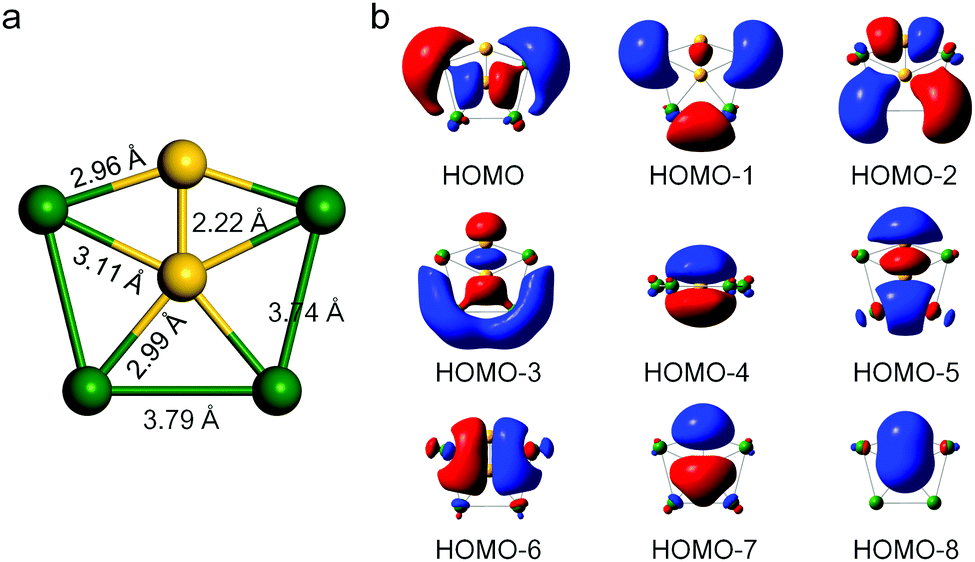 | ||
| Fig. 1 (a) Optimized atomic configuration of a Ca4Si22− molecule computed at the M06-2X/cc-pVTZ level. The yellow and green balls represent Si and Ca atoms, respectively. (b) The canonical molecular orbitals of Ca4Si22−. | ||
The natural population analysis (NPA) charges and the Wiberg bond index (WBI) were then computed at the M06-2X/cc-pVTZ level of theory to understand the bonding characteristics of Ca4Si22−. According to our computations, the ppSi atom is negatively charged (NPA charge −1.55) and the natural electron configuration is 3s1.523px1.053py1.603pz1.34 These results suggest that ppSi in Ca4Si22− is mainly stabilized by the σ-donation of Ca atoms and the delocalization of silicon 3pz electrons. The WBI values for ppSi−Ca bonds are 0.29 and 0.30, respectively, while the WBI of the Si−Si bond is 1.90, resulting in a total WBI of 3.08 for the ppSi center.
To further understand how the ppSi is stabilized in Ca4Si22−, we scrutinized the canonical molecular orbitals of Ca4Si22−. As shown in Fig. 1b, the most occupied molecular orbitals correspond to the σ bonding of ppSi and those between the peripheral Ca and Si atoms. In particular, HOMO−3 is a highly delocalized π orbital and HOMO−4 is a delocalized σ orbital, which could intrinsically help maintain the planar configuration. Interestingly, the number of π electrons in Ca4Si22− satisfies the Hückel (4n + 2) π-electron rule (n = 0), revealing the aromaticity of Ca4Si22−. Moreover, the considerable HOMO–LUMO gap (2.12 eV) also suggests the high stability of Ca4Si22−. Interestingly, the Ca4Si22− anion can be neutralized by two protons (H+) to form a neutral molecule of Ca4Si2H2, which is a local minimum with the lowest vibrational frequency of 26.4 cm−1. In contrast to Ca4Si22−, Ca4Si2H2 has a slightly buckled rather than planar configuration (Fig. S1, ESI†).
Geometric structure of the CaSi monolayer
Inspired by the bonding pattern of ppSi-containing Ca4Si22−, we designed a new ppSi-featuring 2D material, namely a CaSi monolayer. As shown in Fig. 2a, the unit cell of a CaSi monolayer consists of four Si atoms and four Ca atoms in a rectangular shape, with the lattice parameters a and b being 9.33 and 6.86 Å, respectively, optimized using the PBE functional (a = 9.39 Å and b = 6.91 Å by the HSE06 functional). In the CaSi monolayer, each Si atom binds with one Si atom and four Ca atoms nearly in the same plane, forming a quasi ppSi moiety akin to Ca4Si22−. Interestingly, in the CaSi monolayer, each ppSi atom also serves as a ligand of its neighboring ppSi atom. Therefore, the CaSi monolayer can be regarded as a result of embedding Si–Si dimers into the distorted Ca hexagonal lattice.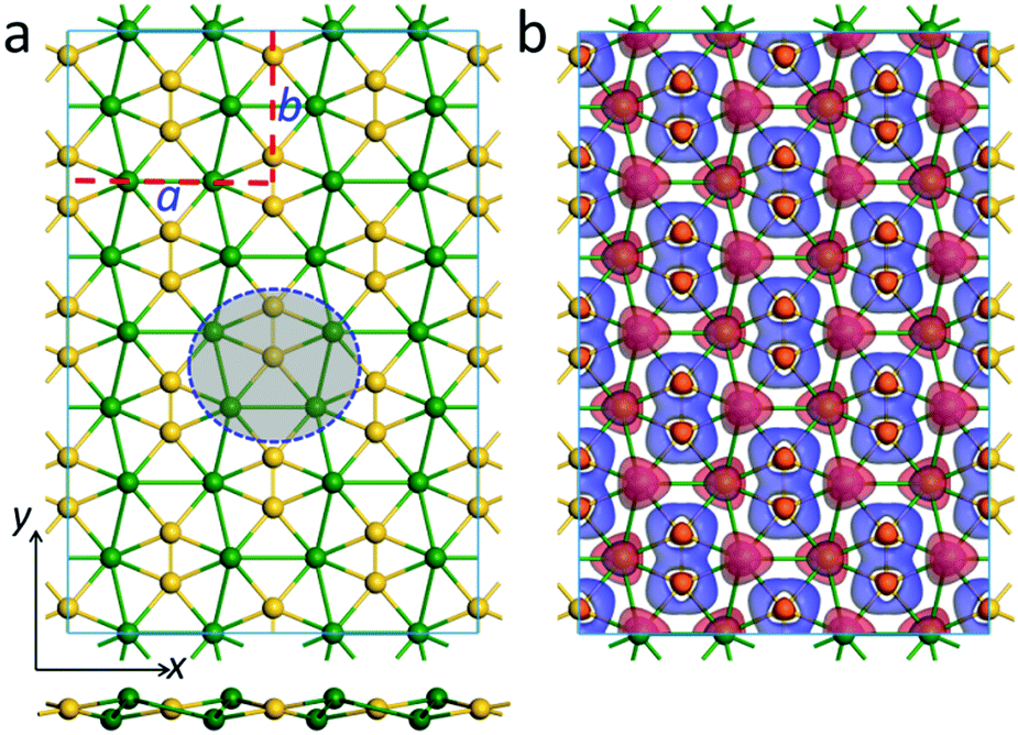 | ||
| Fig. 2 (a) Top (top) and side (bottom) views of an optimized geometric structure of the CaSi monolayer. The red dashed lines label a unit cell, and a and b represent the lattice vectors. The blue dashed circle denotes a Ca4Si2 motif. (b) Deformation electron density of the CaSi monolayer computed using the PBE functional. Blue and red represent electron accumulation and depletion regions, respectively. | ||
Similar to our previously designed phC-containing Be2C monolayer34 and ppC-containing Be5C2 monolayer,33 the CaSi monolayer is not purely planar. As can be seen from the side view (Fig. 2a), the Ca atoms of the CaSi monolayer are buckled into two different atomic layers, which are 0.38 Å above or below the Si atomic layer, respectively. The sum of the three Ca–Si–Ca angles and two Ca–Si–Si angles associated with one ppSi is 364.44°, which is quite close to the ideal 360°, indicating the good planarity of ppSi moieties in the 2D CaSi monolayer. The lengths of the Si–Ca (2.97 Å, 3.04 Å) and Si–Si bonds (2.27 Å) of the CaSi monolayer are quite close to those of Ca4Si22−, whereas the Ca–Ca bond lengths (3.61 Å, 3.98 Å) depart a little from those of Ca4Si22−. Interestingly, the CaSi monolayer can be entirely planar by applying a biaxial tensile strain of 3.4%. However, this purely planar structure is 16 meV per atom higher in energy than the buckled one. According to the Hirshfeld charge population analysis, in the CaSi monolayer, the Si and Ca atoms possess −0.25 |e| and 0.25 |e| charge, respectively. The out-of-plane buckling in the CaSi monolayer could minimize the repulsive interactions between Ca cations and maintain the intensities of the in-plane Si–Ca and Si–Si bonds, which are favorable for the stabilization of the whole structure.
To understand the unique chemical bonding and the stabilizing mechanism of ppSi moieties in the 2D CaSi monolayer, we first plotted its deformation electronic density, which is defined as the difference between the total electronic density and the electronic densities of the isolated Si and Ca atoms. Significant electron transfer occurs from the 4s orbital of the Ca atoms to Si atoms (Fig. 2b), which are delocalized over the Si–Si and Ca–Si bonds, contributing to the stabilization of the ppSi moieties. Moreover, some electrons are also extracted from the 3pz of the Si atoms to further stabilize the ppSi moieties. A similar stabilization mechanism has also been revealed in other 2D nanomaterials with planar hypercoordinate motifs.29–37
To give a more robust analysis of chemical bonding and to understand in more detail how the lattice bonds of the CaSi monolayer are formed, we further employed the recently developed SSAdNDP method to analyze the CaSi monolayer. According to the SSAdNDP analysis (Fig. S2, ESI†), one unit cell of the CaSi monolayer contains two 2c-2e Si–Si bonds, eight 3c-2e σ bonds on eight Ca–Si–Ca triangles, and two 4c-2e π bonds on two Ca–Si–Ca–Si rhombuses, accounting for 24 valence electrons per unit cell. Noteworthily, the two Si atoms and two Ca atoms involved in a 4c-2e π bond are exactly in the same plane. The deduced bonding picture is consistent with the symmetry of the 2D network. Therefore, it is the existence of multicenter delocalized σ and π bonds that help in maintaining the quasiplanar configuration of the CaSi monolayer.
Stability
Although the CaSi monolayer has quite charming topological properties and some intrinsic stabilization factors, physically whether it is a stable structure is still pending. To address this issue, we first computed the cohesive energy of the CaSi monolayer, which is defined as Ecoh = (nESi + nECa − ECaSi)/2n, in which ESi, ECa and ECaSi are the total energies of a single Si atom, a single Ca atom, and the CaSi monolayer, respectively, and n is the number of Si/Ca atoms in the supercell. Physically, the cohesive energy is a reasonable descriptor for the binding strength of connected frameworks. Though smaller than that of the CaSi Zintl phase (3.77 eV per atom), the cohesive energy of the CaSi monolayer (3.07 eV per atom) is comparable to those of the experimentally realized 2D silicene (3.91 eV per atom),50 germanene (3.24 eV per atom),51 and stanene (2.73 eV per atom)52 computed at the same theoretical level, indicating the strongly bonded CaSi monolayer.The kinetic stability of the CaSi monolayer can be confirmed by the phonon curves where no appreciable imaginary phonon mode is observed (Fig. 3). Remarkably, the highest frequency of the CaSi monolayer (475 cm−1) is even higher than those in a MoS2 monolayer (473 cm−1)53 and Cu2Si monolayer (420 cm−1),36 but lower than that of silicene (550 cm−1).54 According to the analysis of the phonon density of states, the highest frequency modes of the CaSi monolayer mainly correspond to the Si–Si bonds. Note that the purely planar CaSi monolayer achieved by a biaxial tensile strain of 3.4% is also dynamically stable as all phonon branches are positive in the entire Brillouin zone (Fig. S3, ESI†).
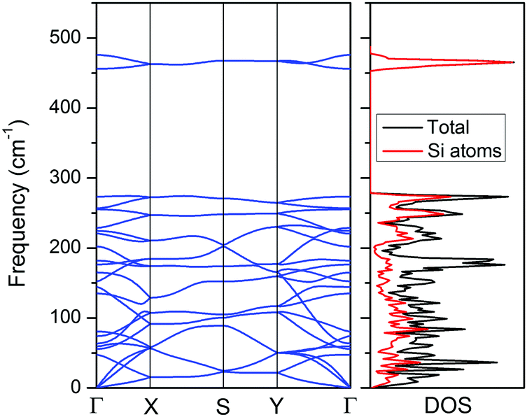 | ||
| Fig. 3 Phonon spectrum (left) and phonon density of states (right) of the CaSi monolayer computed using the PBE functional. | ||
Moreover, we also performed first-principles molecular dynamics (FPMD) simulations to evaluate the thermal stability of the CaSi monolayer. Three independent FPMD simulations (900, 1200, and 1500 K) were carried out using a 3 × 4 supercell. As shown in Fig. S4 (ESI†), the CaSi monolayer can retain its structural integrity with slight out-of-plane distortions throughout a 10 ps FPMD simulation up to 1200 K, suggesting that the ppSi-featuring 2D CaSi phase can be separated by an enough barrier from other minimum structures on the potential energy surface, indicative of good thermal stability. In addition, we performed geometry optimizations starting from the distorted structures by FPMD at 900 K and 1200 K and found that these two structures can easily recover to their initial configurations, indicative of high phase stability.
The aforementioned results can guarantee that the CaSi monolayer is at least a good local minimum structure on the potential energy surface. Experimentally, the global minimum structures have more opportunities to be synthesized than other local minima. Is the ppSi-containing CaSi monolayer the global minimum? To address this issue, we performed a global minimum search for CaSi in the whole 2D space employing the particle-swarm optimization (PSO) method as implemented in the CALYPSO code. As a benchmark, CALYPSO predicted the graphene and h-BN monolayer structures with two-atom hexagonal unit cells by only one generation, suggesting the reliability and efficiency of the PSO algorithm in predicting stable 2D structures.
For 2D CaSi, we obtained three low-energy isomers within 30 generations, which are labeled as CaSi-I, CaSi-II, and CaSi-III (Fig. S5, ESI†). Actually, CaSi-I is just the ppSi-containing CaSi monolayer as discussed above. The structure of CaSi-II can be described as Si tetramers embedded in distorted Ca octagons. Interestingly, all the Si atoms in CaSi-II are also quasi ppSi. In contrast to CaSi-I and CaSi-II, each Si atom in CaSi-III binds with four neighboring Ca atoms to form a ptSi moiety. According to DFT computations, CaSi-I is 86 and 392 meV per atom lower in energy than CaSi-II and CaSi-III, respectively. Therefore, our designed CaSi monolayer is actually the global minimum structure in 2D space, which is the first global minimum of ppSi-containing species. We propose that a CaSi monolayer may be grown on suitable substrates by the chemical vapor deposition (CVD) or molecular beam epitaxy (MBE) method, similar to growing silicene50 and germanene51 on metal or metal oxide surfaces.
Electronic and optical properties
After proving that the CaSi monolayer is a stable structure with fantastic bonding frameworks, we are rather curious if this 2D sheet exhibits some intriguing properties. To this end, we first computed the band structure and density of states (DOS) of the CaSi monolayer to assess its electronic properties. As shown in Fig. 4a, an indirect band gap of 0.50 eV (0.07 eV by the PBE functional, which tends to underestimate the band gap, Fig. S6, ESI†) appears in the band structure of the CaSi monolayer. The valance band maximum (VBM) and conduction band minimum (CBM) are located at the G (0, 0, 0) point and S (0.5, 0.5, 0) point, respectively. Therefore, different from silicene and other theoretically predicted Si-containing 2D structures (e.g. SiC2,35 Cu2Si,36 SiBx,55 SiTix56) which are semimetallic or metallic, the CaSi monolayer is semiconducting with a considerable band gap. Noteworthily, the direct band gap which lies in the Y–G path (0.82 eV) is quite close to the indirect one. Note that the band gaps of most experimentally realized 2D semiconductors, such as BN,57 MoS2,58 and phosphorene,59 are all higher than 1.50 eV, whereas the 2D structures with a band gap in the 0.3–1.5 eV range are highly desirable in the semiconductor industry.60 Since the CaSi monolayer has a rather suitable band gap, once synthesized it would find many important applications in electronics and optoelectronics. More interestingly, if all the atoms of the CaSi monolayer were forced into the same plane, the band gap (0.77 eV, Fig. S7, ESI†) persists, indicating the robust semiconducting properties of the CaSi monolayer.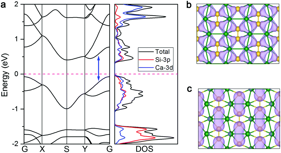 | ||
| Fig. 4 (a) Band structure and density of states (DOS) of CaSi computed using the HSE06 functional. The Fermi level is assigned to zero. The blue double-headed arrow denotes the direct band gap. Partial charge densities for the VBM (b) and CBM (c) of the CaSi monolayer. | ||
The partial DOS analysis demonstrates that the electronic states near the Fermi level of the CaSi monolayer are mainly contributed by the Si-3p and Ca-3d orbitals. It manifests that the empty Ca-3d orbitals split in the CaSi monolayer, and there is a finite probability for Si to back donate some of its received electrons to the low-lying 3d orbitals of Ca, leading to a partial occupancy of 3d orbitals and strong p–d hybridization. This electron donation/back-donation mechanism essentially helps in stabilizing the 2D CaSi network. We also plotted the partial charge densities associated with the VBM and CBM of the CaSi monolayer to give a more explicit picture of its electronic structure. As shown in Fig. 4b and c, the VBM and CBM of the CaSi monolayer are mainly contributed by the multicenter bonding and anti-bonding between Si and Ca atoms, respectively.
The moderate band gap would make the CaSi monolayer a suitable candidate for optoelectronics. To give an intuitive demonstration of the optical properties, we also computed the imaginary part of the dielectric function (ε2)61 of the CaSi monolayer using the HSE06 functional (the PBE results are shown in Fig. S8, ESI†). As shown in Fig. 5, the optical absorption of the CaSi monolayer along the x and y directions covers both the visible and ultraviolet light regions. Remarkably, the absorption along the y direction is much stronger than that of the x direction. In comparison to the x and y directions, the optical absorption along the z direction is much less pronounced. The above results indicate that the CaSi monolayer possesses good capacity for light-harvesting and has unique optical anisotropy.
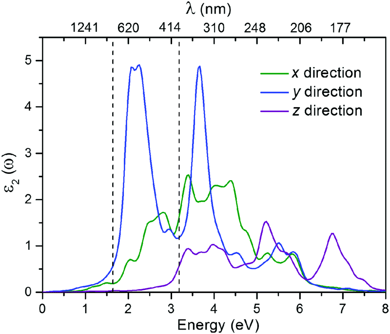 | ||
| Fig. 5 Imaginary dielectric functions of the CaSi monolayer along the x, y and z directions computed using the HSE06 functional. The black dashed lines divide the light spectrum into the infrared, visible, and ultraviolet regions (from left to right). | ||
Mechanical properties
We also assessed the mechanical properties of the CaSi monolayer by computing its elastic constants (Cij). In accordance with the Born criteria,62 a mechanically stable 2D structure should satisfy C11C22 − C122 > 0 and C66 >0. For small external strains ε near the equilibrium positions, the elastic energy Uε can be expressed as:| Uε = Eε – E0 = ½C11εx2 + ½C22εy2 + C12εxεy + 2C66εxy2 | (1) |
On the basis of derived elastic constants, the in-plane Young's modulus (Y) of the CaSi monolayer can be computed by Yx = (C11C22 − C12C21)/C22 = 21.83 N m−1 and Yy = (C11C22 − C12C21)/C11 = 24.61 N m−1, which are much lower than those of graphene (∼341 N m−1)63 and a MoS2 monolayer (∼128 N m−1),64 suggesting that the CaSi monolayer is a rather soft material with good flexibility. The small difference in Young's modulus in different directions indicates that the CaSi monolayer is mechanically anisotropic to a rather small extent.
Remarkably, the negative C12 of the CaSi monolayer leads to negative Poisson's ratios of −0.15 (C21/C22) and −0.16 (C12/C11) in the x and y directions, respectively. Physically, the Poisson's ratio is defined as the negative ratio of the transverse contraction to the longitudinal extension. In nature, most common materials have positive Poisson's ratios as they will become thinner in cross section when they are stretched. Materials with negative Poisson's ratios, which are known as auxetic materials,65 can expand laterally when stretched. As a verification, we found that the equilibrium lattice constant of the CaSi monolayer in the y(X) directions is stretched by ∼0.3% when the lattice is subjected to a tensile strain of 2% in the x(y) direction (Fig. 6), confirming the negative Poisson's ratio of the CaSi monolayer.
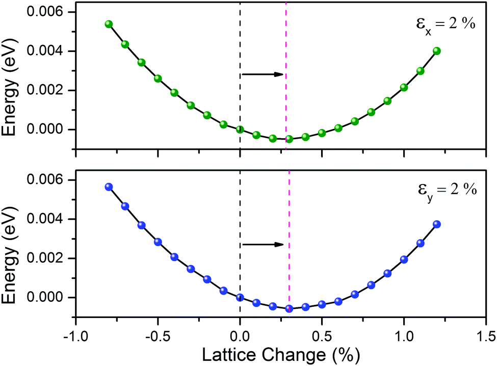 | ||
| Fig. 6 Relative energy as a function of the lattice change along the y (upper) and x (bottom) directions when the CaSi monolayer is subjected to a 2% tensile strain along the x and y directions, respectively. The initial and equilibrium magnitudes of the lattice constant changes are highlighted as black and red dashed lines, respectively. | ||
The negative Poisson's ratio would endow the CaSi monolayer with multiple merits, such as enhanced toughness, self-adaptive vibrational damping and improved shear stiffness. With so fascinating mechanical properties, the CaSi monolayer can be utilized in many specific fields, e.g. superior dampers, piezocomposites, and nanoauxetic materials. Recently, 2D black phosphorus has been first predicted theoretically66 and then observed experimentally67 to have a negative Poisson's ratio. Some hypothetical 2D nanostructures, including but not limited to penta-graphene,68 borophane,69 silica70 and our previously designed Be5C2 monolayer,33 were also revealed to possess a negative Poisson's ratio. Note that the negative Poisson's ratios of black phosphorus and borophane were observed in the out-of-plane direction, while the negative Poisson's ratio of our CaSi monolayer was found in the in-plane direction. Remarkably, the negative Poisson's ratio of the CaSi monolayer is much higher than those of black phosphorus, penta-graphene and borophane, and is comparable to those of silica and a Be5C2 monolayer. No doubt, the unusually negative Poisson's ratios in these 2D structures should be derived from their novel atomic configurations.
Conclusions
To summarize, inspired by the bonding pattern of Ca4Si22−, a local minimum containing a ppSi center, we designed a new 2D material, namely a CaSi monolayer, by means of comprehensive DFT computations. In the CaSi monolayer, each Si atom binds with four Ca atoms and one neighboring Si atom in almost the same plane, forming a quasi ppSi moiety. The CaSi monolayer has rather high thermodynamic, kinetic and thermal stabilities, and is the lowest-energy structure on the 2D energy potential surface. The fundamental mechanism of stabilizing ppSi in the CaSi monolayer is due to the electron donation/back-donation between Si and Ca atoms. Superior to semimetallic silicene, the CaSi monolayer is semiconducting with an indirect band gap of 0.5 eV. It has rather strong optical absorption in the visible and infrared regions of the solar spectrum. In particular, the CaSi monolayer exhibits a rather unusually negative Poisson's ratio. With the development of experimental techniques for the fabrication of 2D materials, we believe that a CaSi monolayer can be achieved in the laboratory in the near future, and its excellent properties and potential applications can be explored. Our work once again highlights the structure–property relationship of materials, and we hope that our work could stimulate more theoretical and experimental efforts towards designing new materials with rule-breaking chemical bonding.Conflicts of interest
There are no conflicts to declare.Acknowledgements
Support in China from the National Natural Science Foundation of China (No. 21522305 and 21403115), the NSF of Jiangsu Province of China (No. BK20150045) and the Innovation Project in Jiangsu Province (KYZZ16_0454), and in USA by NSF-CREST Center for Innovation, Research and Education in Environmental Nanotechnology (CIRE2N) (Grant Number HRD-1736093) and NASA (Grant 17-EPSCoRProp-0032) is gratefully acknowledged. The computational resources utilized in this research were provided by the Shanghai Supercomputer Center.References
- J. H. van't Hoff, Arch. Neerl. Sci. Exactes Nat., 1874, 445 Search PubMed.
- J. A. LeBel, Bull. Soc. Chim. Fr., 1874, 22, 337 Search PubMed.
- H. J. Monkhorst, Chem. Commun., 1968, 1111 RSC.
- R. Hoffmann, R. W. Alder and C. F. Wilcox, J. Am. Chem. Soc., 1970, 92, 4992 CrossRef CAS.
- J. B. Collins, J. D. Dill, E. D. Jemmis, Y. Apeloig, P. v. R. Schleyer, R. Seeger and J. A. Pople, J. Am. Chem. Soc., 1976, 98, 5419 CrossRef CAS.
- F. A. Cotton and M. Millar, J. Am. Chem. Soc., 1977, 99, 7886 CrossRef CAS.
- P. v. R. Schleyer and A. I. Boldyrev, J. Chem. Soc., Chem. Commun., 1991, 1536 RSC.
- A. I. Boldyrev and J. Simons, J. Am. Chem. Soc., 1998, 120, 7967 CrossRef CAS.
- W. Siebert and A. Gunale, Chem. Soc. Rev., 1999, 28, 367 RSC.
- G. Merion, M. A. Mendez-Rojas, A. Vela and T. Heine, J. Comput. Chem., 2007, 28, 362 CrossRef PubMed.
- L.-M. Yang, E. Ganz, Z. Chen, Z.-X. Wang and P. V. R. Schleyer, Angew. Chem., Int. Ed., 2015, 54, 9468 CrossRef CAS PubMed.
- X. Li, L.-S. Wang, A. I. Boldyrev and J. Simons, J. Am. Chem. Soc., 1999, 121, 6033 CrossRef CAS.
- X. Li, H. F. Zhang, L. S. Wang, G. D. Geske and A. I. Boldyrev, Angew. Chem., Int. Ed., 2000, 39, 3630 CrossRef CAS PubMed.
- L. S. Wang, A. I. Boldyrev, X. Li and J. Simons, J. Am. Chem. Soc., 2000, 122, 7681 CrossRef CAS.
- Z. X. Wang and P. v. R. Schleyer, Science, 2001, 292, 2465 CrossRef CAS PubMed.
- Y. Pei, W. An, K. Ito, P. V. R. Schleyer and X. C. Zeng, J. Am. Chem. Soc., 2008, 130, 10394 CrossRef CAS PubMed.
- K. Exner and P. v. R. Schleyer, Science, 2000, 290, 1937 CrossRef CAS PubMed.
- K. Ito, Z. F. Chen, C. Corminboeuf, C. S. Wannere, X. H. Zhang, Q. S. Li and P. V. R. Schleyer, J. Am. Chem. Soc., 2007, 129, 1510 CrossRef CAS PubMed.
- M. B. Krogh-Jesperson, J. Chanderasekhar, E.-U. Würthwein, J. B. Collins and P. V. R. Schleyer, J. Am. Chem. Soc., 1980, 102, 2263 CrossRef.
- E.-U. Würthwein and P. v. R. Schleyer, Angew. Chem., Int. Ed., 1979, 18, 553 CrossRef.
- A. I. Boldyrev, P. v. R. Schleyer and R. Keese, Mendeleev Commun., 1992, 2, 93 CrossRef.
- P. Belanzoni, G. Giorgi, G. F. Cerofolini and A. Sgamellotti, J. Phys. Chem. A, 2006, 110, 4582 CrossRef CAS PubMed.
- A. I. Boldyrev, X. Li and L. S. Wang, Angew. Chem., Int. Ed., 2000, 39, 3307 CrossRef CAS PubMed.
- S. D. Li, C.-Q. Miao, J.-C. Guo and G.-M. Ren, J. Am. Chem. Soc., 2004, 126, 16227 CrossRef CAS PubMed.
- R. Islas, T. Heine, K. Ito, P. V. R. Schleyer and G. Merino, J. Am. Chem. Soc., 2007, 129, 14767 CrossRef CAS PubMed.
- P. D. Pancharatna, M. A. Mendez-Rojas, G. Merino, A. Vela and R. Hoffmann, J. Am. Chem. Soc., 2004, 126, 15309 CrossRef CAS PubMed.
- L. M. Yang, Y. H. Ding and C. C. Sun, J. Am. Chem. Soc., 2007, 129, 658 CrossRef CAS PubMed.
- M. H. Wu, Y. Pei and X. C. Zeng, J. Am. Chem. Soc., 2010, 132, 5554–5555 CrossRef CAS PubMed.
- X. J. Wu, Y. Pei and X. C. Zeng, Nano Lett., 2009, 9, 1577 CrossRef CAS PubMed.
- Z. Zhang, X. Liu, B. I. Yakobson and W. Guo, J. Am. Chem. Soc., 2014, 133, 19326 Search PubMed.
- Y. Li, Y. Liao, P. V. R. Schleyer and Z. Chen, Nanoscale, 2014, 6, 10784 RSC.
- J. Dai, X. Wu, J. Yang and X. C. Zeng, J. Phys. Chem. Lett., 2014, 5, 2058 CrossRef CAS PubMed.
- Y. Wang, F. Li, Y. Li and Z. Chen, Nat. Commun., 2016, 7, 11488 CrossRef CAS PubMed.
- Y. Li, Y. Liao and Z. Chen, Angew. Chem., Int. Ed., 2014, 53, 7248 CrossRef CAS PubMed.
- Y. Li, F. Li, Z. Zhou and Z. Chen, J. Am. Chem. Soc., 2011, 133, 900 CrossRef CAS PubMed.
- L.-M. Yang, V. Bači, I. A. Popov, A. I. Boldyrev, T. Heine, T. Frauenheim and E. Ganz, J. Am. Chem. Soc., 2015, 137, 2757 CrossRef CAS PubMed.
- B. Feng, B. Fu, S. Kasamatsu, S. Ito, P. Cheng, C. Liu, Y. Feng, S. Wu, S. K. Mahatha, P. Sheverdyaeva, P. Moras, M. Aritam, O. Sugino, T. Chiang, K. Shimada, K. Miyamoto, T. Okuda, K. Wu, L. Chen., Y. Yao and I. Matsuda, Nat. Commun., 2016, 8, 1007 CrossRef PubMed.
- Y. Zhao and D. G. Truhlar, Theor. Chem. Acc., 2008, 120, 215 CrossRef CAS.
- M. J. Frisch, et al., GAUSSIAN 03, Revision E.02, Gaussian, Inc., Wallingford, CT, 2004, see the ESI for the full reference Search PubMed.
- J. A. Pople, M. Head-Gordon and K. Raghavachari, J. Chem. Phys., 1987, 87, 5968 CrossRef CAS.
- G. Kresse and J. Hafner, Phys. Rev. B: Condens. Matter Mater. Phys., 1993, 47, 558 CrossRef CAS.
- J. P. Perdew, L. Burke and M. Ernzerhof, Phys. Rev. Lett., 1996, 77, 3865 CrossRef CAS PubMed.
- P. E. Blöchl, Phys. Rev. B: Condens. Matter Mater. Phys., 1994, 50, 17953 CrossRef.
- G. Kresse and D. Joubert, Phys. Rev. B: Condens. Matter Mater. Phys., 1999, 59, 1758 CrossRef CAS.
- J. Heyd, G. E. Scuseria and M. Ernzerhof, J. Chem. Phys., 2006, 124, 219906 CrossRef.
- A. Togo, F. Oba and I. Tanaka, Phys. Rev. B: Condens. Matter Mater. Phys., 2008, 78, 134106 CrossRef.
- T. R. Galeev, B. D. Dunnington, J. R. Schmidt and A. I. Boldyrev, Phys. Chem. Chem. Phys., 2013, 15, 5022 RSC.
- G. J. Martyna, M. L. Klein and M. E. Tuckerman, J. Chem. Phys., 1992, 97, 2635 CrossRef.
- Y. Wang, J. Lv, L. Zhu and Y. Ma, Phys. Rev. B: Condens. Matter Mater. Phys., 2010, 82, 094116 CrossRef.
- P. Vogt, P. D. Padava, C. Quaresima, J. Avila, E. Frantzeskakis, M. C. Asensio, A. Resta, B. Ealet and G. L. Lay, Phys. Rev. Lett., 2012, 108, 155501 CrossRef PubMed.
- L. Li, S. Lu, J. Pan, Z. Qin, Y. Wang, Y. Wang, G. Cao, S. Du and H. Gao, Adv. Mater., 2014, 25, 4820 CrossRef PubMed.
- F. Zhu, W. Chen, Y. Xu, C. Gao, D. Guan, C. Liu, D. Qian, S.-C. Zhang and J. Jia, Nat. Mater., 2015, 14, 1020 CrossRef CAS PubMed.
- A. Molina-Sánchez and L. Wirtz, Phys. Rev. B: Condens. Matter Mater. Phys., 2011, 84, 155413 CrossRef.
- S. Cahangirov, M. Topsakal, E. Akturk, H. Sahin and S. Ciraci, Phys. Rev. Lett., 2009, 102, 236804 CrossRef CAS PubMed.
- J. Dai, Y. Zhao, X. Wu, J. Yang and X. Zeng, J. Phys. Chem. Lett., 2013, 4, 561 CrossRef CAS PubMed.
- Q. Wu, J.-J. Zhang, P. Hao, Z. Ji, S. Dong, C. Ling, Q. Chen and J. Wang, J. Phys. Chem. Lett., 2016, 7, 3723 CrossRef CAS PubMed.
- A. Nag, K. Raidongia, K. P. S. S. Hembram, R. Datta, U. V. Waghmare and C. N. R. Rao, ACS Nano, 2010, 4, 1539 CrossRef CAS PubMed.
- K. F. Mak, C. Lee, J. Hone, J. Shan and T. F. Heinz, Phys. Rev. Lett., 2010, 105, 136805 CrossRef PubMed.
- L. Li, Y. Yu, G. J. Ye, Q. Ge, X. Ou, H. Wu, D. Feng, X. H. Chen and Y. Zhang, Nat. Nanotechnol., 2014, 9, 372 CrossRef CAS PubMed.
- L. Li, J. Kim, C. Jin, G. J. Ye, D. Y. Qiu, F. H. Da Jornada, Z. Shi, L. Chen, Z. Zhang, F. Yang, K. Watanabe, T. Taniguchi, W. Ren, S. G. Louie, X. H. Chen, Y. Zhang and F. Wang, Nat. Nanotechnol., 2017, 12, 21 CrossRef CAS PubMed.
- M. Gajdoš, K. Hummer and G. Kresse, Phys. Rev. B: Condens. Matter Mater. Phys., 2006, 73, 045112 CrossRef.
- M. Born and H. Huang, Dynamical theory of crystal lattices, Clarendon, Oxford, 1954 Search PubMed.
- Q. Peng, X. Wen and S. De, RSC Adv., 2013, 3, 13772 RSC.
- Y. Cai, G. Zhang and Y.-W. Zhang, J. Am. Chem. Soc., 2014, 136, 6269–6275 CrossRef CAS PubMed.
- R. S. Lakes, Science, 1987, 235, 1038 CAS.
- J. W. Jiang and H. S. Park, Nat. Commun., 2014, 5, 4727 CAS.
- Y. Du, J. Maassen, W. Wu, Z. Luo, X. Xu and P. D. Ye, Nano Lett., 2016, 16, 6701 CrossRef CAS PubMed.
- S. Zhang, J. Zhou, Q. Wang, X. Chen, Y. Kawazoe and P. Jena, Proc. Natl. Acad. Sci. U. S. A., 2015, 112, 2372 CrossRef CAS PubMed.
- L. Kou, Y. Ma, C. Tang, Z. Sun, A. Du and C. Chen, Nano Lett., 2016, 16, 7910 CrossRef CAS PubMed.
- V. O. Özçelik, S. Cahangirov and S. Ciraci, Phys. Rev. Lett., 2014, 112, 246803 CrossRef PubMed.
Footnote |
| † Electronic supplementary information (ESI) available. See DOI: 10.1039/c7nh00091j |
| This journal is © The Royal Society of Chemistry 2018 |