
An effective approach to alleviating the thermal effect in microstripe array-LEDs via the piezo-phototronic effect†
Chunhua
Du‡
a,
Liang
Jing‡
a,
Chunyan
Jiang
a,
Ting
Liu
a,
Xiong
Pu
a,
Jiangman
Sun
a,
Dabing
Li
 *b and
Weiguo
Hu
*a
*b and
Weiguo
Hu
*a
aBeijing Institute of Nanoenergy and Nanosystems, Chinese Academy of Sciences, Beijing, 100083, P. R. China. E-mail: huweiguo@binn.cas.cn
bChangchun Institute of Optics, Fine Mechanics and Physics, Chinese Academy of Sciences, Changchun, 130033, P. R. China. E-mail: lidb@ciomp.ac.cn
First published on 23rd November 2017
Abstract
Micro-LEDs, with unparalleled high brightness compared to conventional LEDs and OLEDs, have been regarded as a research priority for high-power light emitting diodes. Thermal issue is an inevitable concern in LED operation, leading to luminescence degradation and lifetime shortening. Here we studied the role the piezo-phototronic effect played in the luminescence enhancement of microstripe array-LEDs via strain compensation at room temperature. And also, we firstly reveal the effective modulation of the piezo-phototronic effect on luminescence characteristics at high temperatures via EL measurements with the temperature increasing from 300 K to 380 K. Industrial GaN-based high-power LEDs have been reported to be commonly operated in the temperature range of 70–90 °C. Compared to at 300 K, the integrated EL intensity at 364 K decreases to 67.8% without strain; however, by applying a strain of 0.09%, it is demonstrated to rise to as high as 104% of that at 300 K. This work deepens the understanding of the high-temperature piezo-phototronic effect and will give significant guidance for high-power LEDs from the important direction of nitride semiconductors.
Conceptual insightsThe area of micro-LEDs has been a promising, flourishing and remarkable research direction for high-power solid-state lighting using group-III nitride materials. For high-power LEDs, the thermal issue is of great research value, as it causes light output degradation, lifetime shortening and the risk of catastrophic failure when LEDs are in operation. Here we prepared novel microstripe arrayed InGaN/GaN MQW LEDs, where thermal degradation is effectively alleviated via the piezo-phototronic effect. The piezo-phototronic effect is demonstrated to play a great role in the evident enhancement of LED emission efficiency within the temperature range from 300 K to 380 K. Commercial HPLEDs are commonly operated in the temperature range of 70–90 °C. In particular, thermal degradation is demonstrated to be fully compensated upon applying a 0.09% strain at 364 K. This novel easy-to-implement, space-saving and economic method efficiently alleviates thermal degradation in high-power LED operation, which will greatly promote the development of high-performance commercial LEDs. |
1. Introduction
The past decades have witnessed the rapid development of light emitting diodes (LEDs), with applications widely existing in the fields of general lighting, traffic signals, displays, bio-medical treatment, etc.1–4 High-power light emitting diodes (HPLEDs) have been perceived as one of the important future research directions for nitride semiconductors.5–13 Lately, micro-LEDs possessing high brightness have stood out and received dramatic attention from researchers and large enterprises worldwide.7,14,15 However, nearly 80% of the input electrical power is consumed as heat in LEDs because of low electric-photo conversion, leading to heat accumulation issues and thus temperature rises, which will cause accelerated light output degradation and severe lifetime shortening, even risking catastrophic failure.16,17 The lifetime of an LED chip has been predicted to decay exponentially as the temperature increases. The thermal issue is commonly relieved for higher light output via thermal dissipation, through either natural or active means, to keep the chip controlled at as low a temperature as possible.16,18 Nevertheless, the application of these methods has been greatly restricted due to complex structures, low working efficiencies and high costs, meaning the thermal issue is still a challenge.With the three-way coupling of piezoelectric, semiconducting and photoexcitation properties, the piezo-phototronic effect uses a strain-induced piezopotential as a “gate” to control carrier generation, transportation, separation and/or recombination for improving the performance of optoelectronic devices.19–21 The piezo-phototronic effect has promising applications, from visible light communication, solar cells, pressure imaging, and electronic skin, to Boolean logic, computation and luminescence applications, and so on.22–28 With on-going in-depth research into the emission enhancement of LEDs, new insight has also been brought to this through the piezo-phototronic effect, coupled with plasmons and so on, at room temperature.29–31 The effective modulation of the piezo-phototronic effect at temperatures ranging from 300 K down to 77 K has been systemically investigated in nonpolar a-axis GaN.32 However, the high-temperature piezo-phototronic effect, which has important significance for HPLEDs, is quite desirable but there is still a lack of exploration into this.
In this work, microstripe arrayed In0.18Ga0.82N/GaN MQW LEDs are fabricated via traditional photolithography. The role of the piezo-phototronic effect on the electroluminescence (EL) characteristics of the micro-LEDs is investigated. EL measurements at temperatures ranging from 300 K to 380 K are also conducted to systematically study the high-temperature piezo-phototronic effect under practical operation. This work will open up the application of the piezo-phototronic effect in high-temperature circumstances, improving fundamental understanding and also guiding the design and development of high-performance piezo-phototronic devices based on micro/nano-structured piezoelectric semiconductors in the future.
2. Results and discussion
The In0.18Ga0.82N/GaN MQW LEDs used in this work are grown on c-plane sapphire substrates via metalorganic chemical vapor deposition (MOCVD). Fig. 1(a) displays a schematic diagram of the architecture of a microstripe arrayed LED chip. The microstripe array of the In0.18Ga0.82N/GaN MQW structure is fabricated via traditional photolithography, with Cr/Ni/Al and Ni/Au deposited as n-type and p-type electrodes via electron beam evaporation. Typical scanning electron microscope (SEM, Hitachi SU8010) images of the microscale In0.18Ga0.82N/GaN MQW array are displayed in Fig. 1(b), showing a large-area, uniform and well-aligned distribution. The diameter, height and duty cycle of every single stripe are 3 μm, 0.7 μm and 4 μm, respectively. With a square patterned n-electrode throughout the entire n-type layer, current injection into every pixel is uniform. As soon as electrons in n-GaN and holes in p-GaN are simultaneously injected into the MQW region when a forward bias is applied, the transition of electrons from the conduction band into the valence band contributes to generating photons. Fig. 1(c) displays EL spectra from the micro-LEDs measured under various electrical injection currents. Remarkable luminescence enhancement is shown as the injection current increases from 1 mA to 7 mA due to electric-photo conversion. A nearly linear increasing relationship exists between the luminescence intensity and the injection current, as clearly observed in Fig. 1(d). Besides, a slight blue-shift of the luminescence peak occurs with the increase in injection current, which is ascribed to the screening effect of carriers on the strong lattice-mismatch induced internal piezoelectric field along the polar [0001]-axis.9,33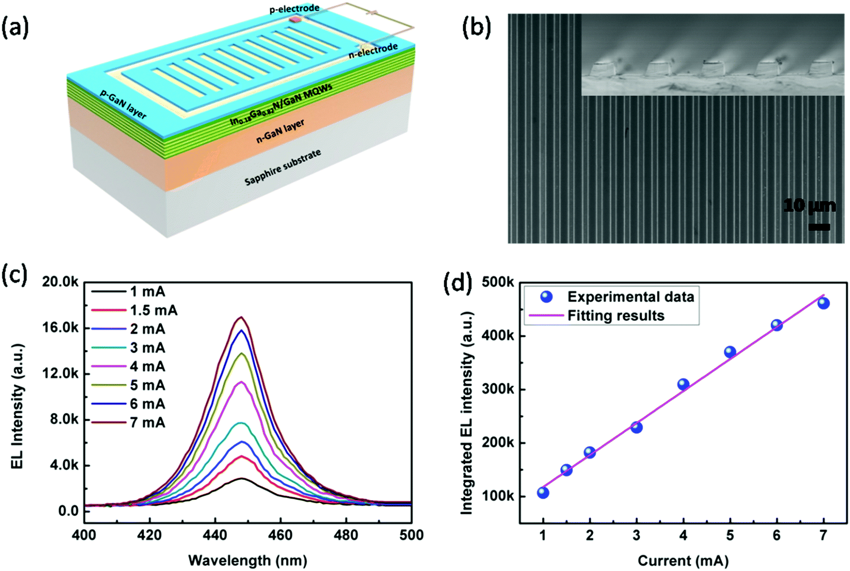 | ||
| Fig. 1 EL performance measurements of microstripe arrayed In0.18Ga0.82N/GaN MQW LEDs at room temperature. (a) A schematic diagram of the microstripe arrayed In0.18Ga0.82N/GaN MQW LED system. (b) Top view and cross-section (inset) SEM images of the microstripe array structure. (c) EL spectra under a series of currents. (d) The integrated EL intensity as a function of injection current. The pink line is the fitting of the experimental data. | ||
The modulation by the piezo-phototronic effect on the luminescence characteristics of the In0.18Ga0.82N/GaN microstripe array-LED at room temperature is systematically studied under various straining conditions, as shown in Fig. 2 and 3. External strain is applied on the chip via the screwing-in of the jackscrew when it is fixed on a jig, which is the same case as in our previous work.34,35 The existence of strain on the In0.18Ga0.82N/GaN microstripe array along the c-axis direction as a result of mechanical deformation is calculated via finite element analysis (FEA) using COMSOL, as shown in Fig. 2(a). A piezoelectric potential will thus be newly generated at the top and bottom of every individual microstripe unit along the c-axis, due to the central nonsymmetry in the wurtzite structure as strain is applied, which will influence EL electro-optic processes, such as transportation and recombination. EL measurements of the as-fabricated microstripe arrayed LEDs under a series of external strains are conducted, as shown in Fig. 2(b). Under an injection current of 5 mA, an increase in emission intensity is observed, as the external strain increases from 0% up to 0.09%. As shown in the top inset of Fig. 2(b), the integrated intensity under a 0.09% strain is calculated to increase to 134.7% of the value without a strain. As a result of the three-way coupling of the piezoelectric, semiconducting, and photoexcitation properties of piezoelectric semiconductor materials in the wurtzite family, such as ZnO, GaN, and CdS, the piezo-phototronic effect sheds new light on tuning/controlling carrier generation, transport, separation and recombination in optoelectronic devices through piezoelectric charges induced by strain.38–41Fig. 2(c and d) present the calculated energy band profiles and corresponding wave functions of electrons and holes in the In0.18Ga0.82N/GaN microstripe structure without/with strain, based on a self-consistent theoretical model. Therein, interband transition between the first conduction sub-band and the first heavy-hole valence sub-band is considered. As for the as-grown In0.18Ga0.82N/GaN QWs, lattice mismatches between the InGaN and GaN layers result in in-plane compressive and tensile strain, thereby, respectively, positive and negative piezoelectric charges are produced at the top and bottom of the InGaN layer. An electric field along (opposite to) the c-axis is thus created in the InGaN (GaN) layer. As displayed in Fig. 2(c), negative piezo-charges accumulated at the bottom of the InGaN layer bend the energy band upwards, whereas the positive piezo-charges at the top bend the energy band downward, misaligning the wave functions of electrons and holes in the QW, as displayed in Fig. 2(d). The external force/strain applied upon bending the LED chip partially “cancels” the lattice-mismatch induced strain in the InGaN layer, and the piezoelectric charges at the interface are thus counteracted partly, leading to the energy band becoming less tilted. As a consequence, the wave functions of holes and electrons confined in the QW overlap more, causing an increase in the recombination rate and also the emission efficiency of micro-LEDs. This explicitly demonstrates the effective modulation by the piezo-phototronic effect on the luminescence properties of microstripe arrayed In0.18Ga0.82N/GaN LEDs, both experimentally and using calculations. Current–voltage characteristics measured under various strains are shown in the lower inset of Fig. 2(b). The steeper slopes of the I–V curves indicate that the turn-on voltage decreases as the strain increases. There are two possibilities to account for this. Using the simplified theory of Shockley, the total current is given by J = Jp + Jn + Jre.36 Therein, the recombination current, Jre, is inversely proportional to the carrier lifetime, which decreases rapidly as the external strain increases (Fig. 3(b)), while Jp and Jn depend on the diffusion coefficient, diffusion length and carrier doping concentration only. Therefore, the total current is increased as the external strain increases. Furthermore, it is pointed out that the carrier injection efficiency in the junction region is improved due to energy-band restructuring by piezoelectric polarization charges.37
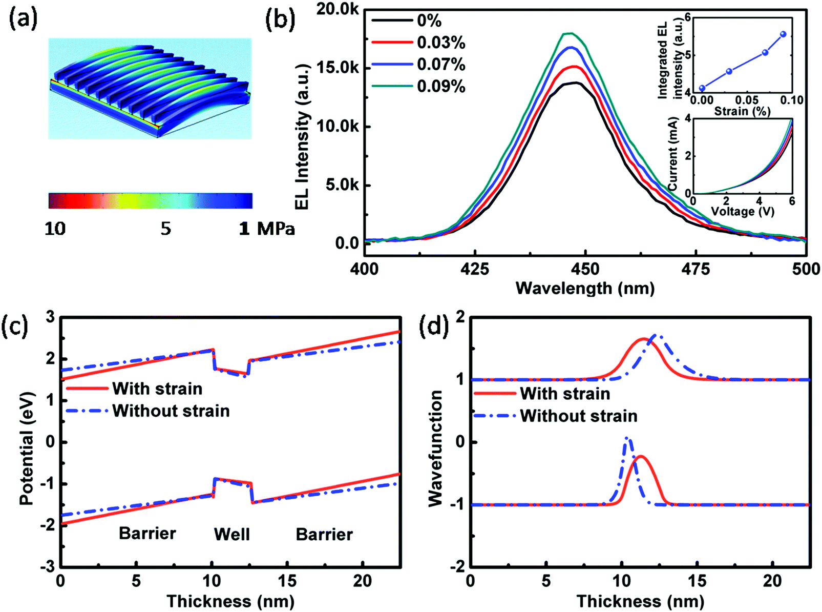 | ||
| Fig. 2 The EL characteristics under various strains at room temperature. (a) The strain distribution on an In0.18Ga0.82N/GaN microstripe array simulated by COMOSOL. (b) EL spectra under an injection current of 5 mA under different strains. The inset at the top shows the integrated EL intensities of micro-LEDs as a function of strain. The inset below shows the current–voltage characteristics of micro-LEDs under various strains. (c) Energy band profiles and (d) wave functions of holes and electrons in QWs with external strain (the red line) and without external strain (the blue dotted line). | ||
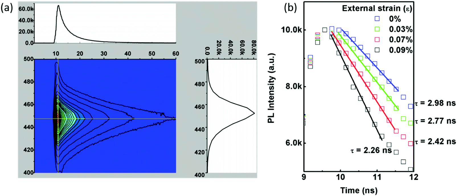 | ||
| Fig. 3 Transient PL spectra measurements of a microstripe arrayed In0.18Ga0.82N/GaN MQW LED. (a) A time-resolution contour plot of the PL spectrum and (b) TRPL spectra under different strains. The solid lines are curves fitted via a single exponential. | ||
The crucial role the piezo-phototronic effect plays on PL optoelectronic processes is also investigated via time-resolution photoluminescence (TRPL) measurements.42,43Fig. 3(a) gives a room-temperature transient-spectral profile of a microstripe arrayed In0.18Ga0.82N/GaN MQW LED over the nanosecond time range. The horizontal axis shows that the intensity of the given emission process exponentially decays with time, following a basic rate equation (as shown in the top panel), and the vertical axis reflects which transition process dominates the light emission at a fixed time (as shown in the right panel).44 In our case, the main emission is always referred to as the transition from the conduction band to the valence band. Fig. 3(b) shows the TRPL decay curves as a function of external strain. Convolution fitting to every individual data point gives rapid single exponential decay. As the strain increases up to 0.09%, the monotonic decrease of PL intensity with time becomes faster and faster, indicating the continuous shortening of carrier lifetime. Lifetimes of 2.98, 2.77, 2.42 and 2.26 ns correspond to PL decay under a strain of 0%, 0.03%, 0.07% and 0.09%, respectively. The shortening of carrier lifetime as strain increases could be deduced from Fig. 2(c and d). The lattice-mismatch induced out-of-plane strain is partially cancelled by the applied external strain in the InGaN layer, leading to the piezoelectric charges at the interface being reduced and the energy band being less tilted. The wave function overlap of the electrons and holes is thus increased, with the radiative recombination rate being increased. Therefore, the TRPL curves decay faster and faster, and the carrier lifetime in the QW becomes smaller and smaller as strain increases, which suggests the effective modulation by the piezo-phototronic effect on the emission enhancement of micro-LEDs.
The EL characteristics of microstripe arrayed In0.18Ga0.82N/GaN MQW LEDs over the temperature range from 300 K to 380 K are extensively studied. Fig. 4(a) shows that the turn-on voltage decreases as the temperature increases, in accordance with the case in conventional LEDs.45Fig. 4(b) displays EL spectra at different temperatures under an injection current of 5 mA, showing a consecutive intensity decreases as the temperature increases, probably due to increased nonradiative recombination behaviour, involving defects, dislocations and Auger recombination, and the decrease of the spontaneous emission rate as well.46,47 A 4.6 nm red-shift in emission wavelength caused by the shrinkage of the energy band as the temperature increases is also demonstrated in Fig. 4(c). The reduction in emission intensity and the wavelength instability of this microstripe arrayed LED at high temperatures does harm to lighting. The unfavorable consequences caused by the thermal effect are traditionally weakened/evaded via heat dissipation for higher emission output during operation, which is mostly inconvenient to implement, space occupying and costly.48 Therefore, a certain easily fabricated, manoeuvrable and economical technique is greatly anticipated.
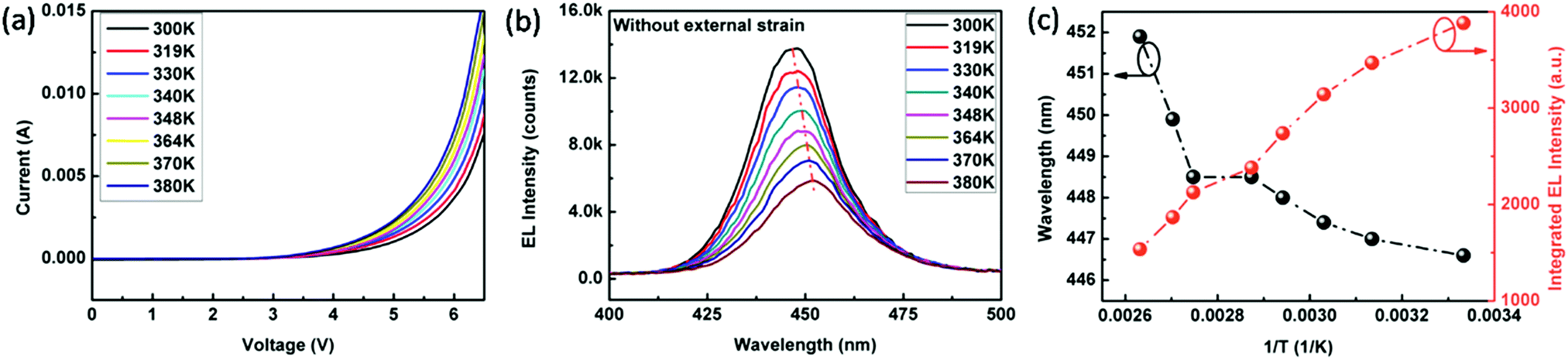 | ||
| Fig. 4 EL characteristic measurements over the temperature range from 300 to 380 K, without external strain, under an injection current of 5 mA. (a) I–V characteristics at different temperatures. (b) EL spectra at different temperatures. (c) The peak wavelength and integrated EL intensity as a function of 1/T. | ||
The temperature dependence of the piezo-phototronic effect modulation of the luminescence characteristics of microstripe arrayed In0.18Ga0.82N/GaN LEDs under various strains is systematically studied in Fig. 5. In this work, external strains are applied to the chip via a stress controller and the temperature is continuously regulated via a heating stage and measured using an infrared thermometer, as shown in Fig. 5(a). EL spectra are measured at 300 (Fig. 5(b)), 319 (Fig. S1a, ESI†), 343 (Fig. S1b, ESI†), 364 (Fig. 5(c)), 370 (Fig. S1c, ESI†) and 380 K (Fig. 5(d)) via externally applying strains under an injection current of 5 mA. It is obviously observed that emission intensities increase as the external strain increases under each temperature condition. This is a result of an enhanced radiative recombination rate in the QWs, due to the weakening of the internal electric field, caused by external-strain induced polarization charges at InGaN/GaN interfaces from the piezo-phototronic effect, as previously discussed. Fig. 5(e) shows the strain dependence of the integrated EL intensities of the LEDs at each temperature. The monotonic increase of the integrated EL intensity as a function of strain at each temperature can be clearly seen. The same variation tendency of the EL properties as the strain increases at temperatures from 300 K to 380 K firstly reveals effective modulation by the piezo-phototronic effect in modifying the energy band profiles and the radiative recombination of hole and electron pairs at high temperatures. As the temperature increases, it is really worth mentioning that the integrated EL intensity at 364 K reduces to 67.8% of that at 300 K when no strain is applied; surprisingly, it actually returns back to as high as 104% of that at 300 K upon applying a strain of 0.09%. 364 K is right in the temperature range of HPLED chip operation.49 Therefore, adequate strain can be introduced in the packaging of LEDs to alleviate the bad consequences of the thermal effect for higher emission outputs, acting as a supplement/alternative to traditional methods focusing on thermal dissipation. The role that the piezo-phototronic effect plays on emission enhancement is crucial for advancing the industrialization of high-performance HPLEDs. LED chips working at temperatures above 380 K will experience irreversible luminescence degradation, which is not discussed here.16,50,51 A contour plot of temperature in Fig. 5(f) clearly displays the temperature dependence of the integrated EL intensity as a function of strain, which will definitely guide the future design of LEDs. This work provides in-depth research into the piezo-phototronic effect, applying a high-temperature range beyond previously reported low temperature and room temperature studies, elaborating a better understanding of the piezo-phototronic effect and effectively relieving the thermal effect for the industrialization of LEDs.
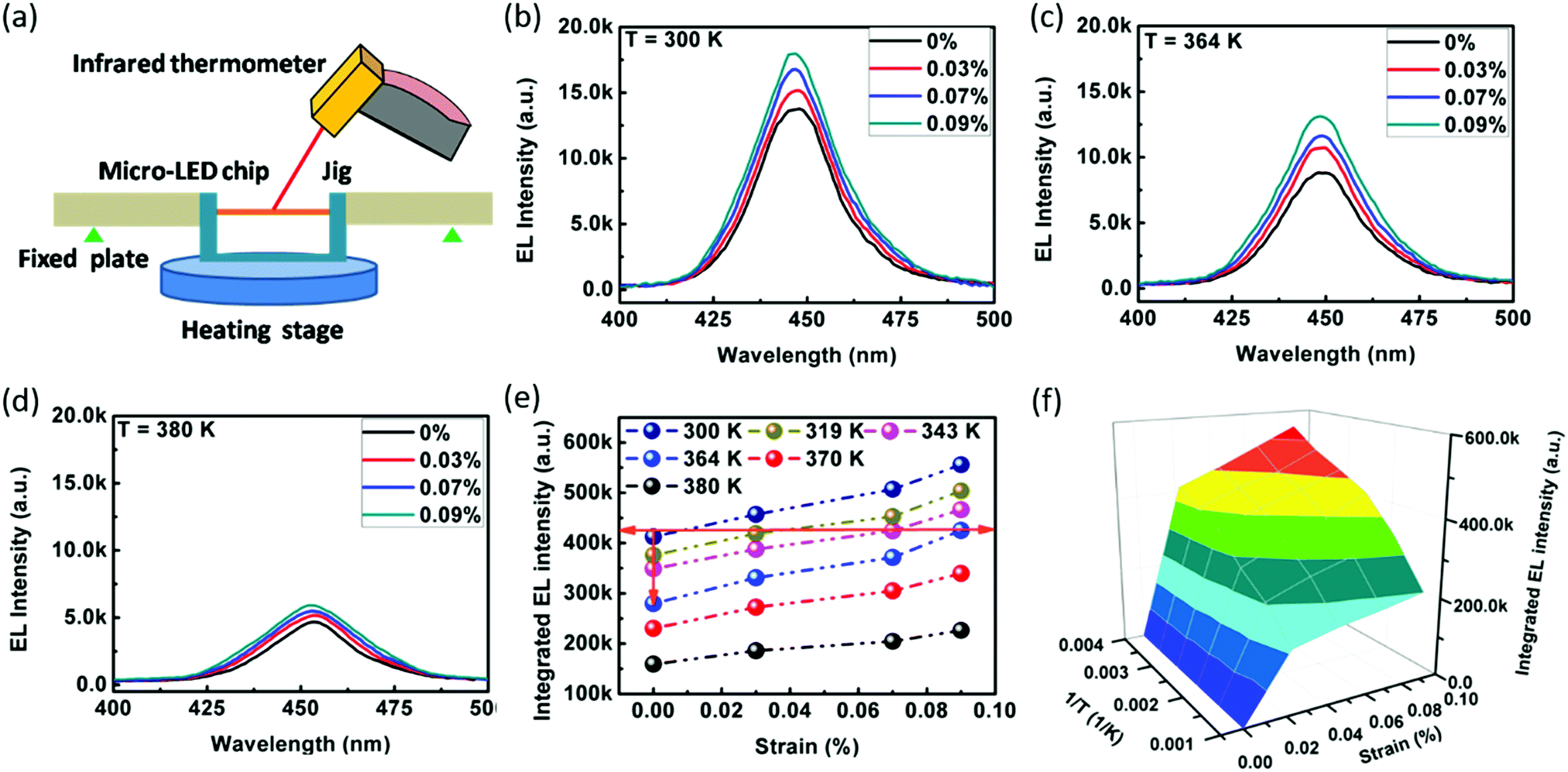 | ||
| Fig. 5 The temperature dependent modulation of the electroluminescence properties of microstripe arrayed In0.18Ga0.82N/GaN MQW LEDs via the piezo-phototronic effect under an injection current of 5 mA. (a) A schematic diagram of the setup for high-temperature EL characteristic measurements. EL spectra of devices at (b) 300 K, (c) 364 K, and (d) 380 K under externally applied strains. (e) The strain dependence of the integrated EL intensity at different temperatures. (f) A contour plot of the temperature dependence of integrated EL intensity as a function of external strain. | ||
3. Conclusions
The piezo-phototronic effect is firstly applied to microstripe array-LEDs as a novel approach to enhance the luminescence characteristics at high temperatures. Strain-induced piezoelectric polarization charges (piezopotential) are utilized to modify energy band profiles in QWs and thus tune/control the quantum transitions of carriers via the piezo-phototronic effect, instead of the previous methods of strengthening heat dissipation for higher emission output. As the temperature increases to 364 K, the integrated EL intensity of the device decreases to 67.8% of that at 300 K. When a strain of 0.09% is applied, the integrated EL intensity at 364 K is demonstrated to be as high as 104% of that at 300 K, which will greatly benefit the advance of HPLEDs. This method is fundamentally new in science and possesses superior advantages in addition to high power output, such as being easy-to-implement, space-saving and economical in alleviating the thermal effect in microstripe arrayed LEDs. This work not only deepens the understanding of the piezo-phototronic effect in nitride semiconductors, but also will give significant guidance in the design of high-performance industrial LEDs.Conflicts of interest
There are no conflicts to declare.Acknowledgements
C. D. and L. J. contributed equally to this work. The authors are thankful for support from the “thousands talents” program for pioneer researcher and his innovation team, China, the National Natural Science Foundation of China (Grant No. 51432005, 61574018, 51603013 and 61704008), the Youth Innovation Promotion Association of the Chinese Academy of Sciences, the “Hundred Talents Program” of the Chinese Academy of Sciences, the National Key Research and Development Program of China (2016YFA0202703), and the National Science Fund for Distinguished Young Scholars (61725403).References
- P. Waltereit, O. Brandt, A. Trampert, H. T. Grahn, J. Menniger, M. Ramsteiner, M. Reiche and K. H. Ploog, Nature, 2000, 406, 865–868 CrossRef CAS PubMed.
- C. Du, Z. Ma, J. Zhou, T. Lu, Y. Jiang, P. Zuo, H. Jia and H. Chen, Appl. Phys. Lett., 2014, 105, 071108 CrossRef.
- T. Lu, Z. Ma, C. Du, Y. Fang, H. Wu, Y. Jiang, L. Wang, L. Dai, H. Jia, W. Liu and H. Chen, Sci. Rep., 2014, 4, 6131 CrossRef CAS PubMed.
- X. M. Zhang, M. Y. Lu, Y. Zhang, L. J. Chen and Z. L. Wang, Adv. Mater., 2010, 21, 2767–2770 CrossRef.
- H. P. T. Nguyen, S. Zhang, K. Cui, X. Han and Z. Mi, 2011 Conference on Lasers and Electro-Optics (CLEO), 2011, pp. 1–2 Search PubMed.
- J. Piprek, IEEE J. Quantum Electron., 2016, 99, 1 Search PubMed.
- C. Zhao, T. K. Ng, R. T. Elafandy, A. Prabaswara, G. B. Consiglio, I. A. Ajia, I. S. Roqan, B. Janjua, C. Shen and J. Eid, Nano Lett., 2016, 16, 4616 CrossRef CAS PubMed.
- A. E. Chernyakov, A. P. Kartashova, N. M. Shmidt and E. I. Shabunina, International Conference on Thermal, 2016, pp. 1–6 Search PubMed.
- G. Harbers, G. Mueller, L. Zhou, M. G. Craford, M. R. Krames, O. B. Shchekin and R. Muellermach, J. Disp. Technol., 2007, 3, 160–175 CrossRef.
- T. Lu, Z. Ma, C. Du, Y. Fang, F. Chen, Y. Jiang, L. Wang, H. Jia and H. Chen, Appl. Phys. A: Mater. Sci. Process., 2014, 114, 1055–1059 CrossRef CAS.
- T. Lu, Z. Ma, C. Du, Y. Fang, F. Chen, Y. Jiang, L. Wang, H. Jia and H. Chen, J. Disp. Technol., 2014, 10, 146–150 CrossRef CAS.
- Y. Zhu, T. Lu, X. Zhou, G. Zhao, H. Dong, Z. Jia, X. Liu and B. Xu, Nanoscale Res. Lett., 2017, 12, 321 CrossRef PubMed.
- X. Rong, X. Wang, S. V. Ivanov, X. Jiang, G. Chen, P. Wang, W. Wang, C. He, T. Wang and T. Schulz, Adv. Mater., 2016, 28, 7978–7983 CrossRef CAS PubMed.
- B. O. Jung, S. Y. Bae, Y. K. Sang, S. Lee, J. Y. Lee, D. S. Lee, Y. Kato, Y. Honda and H. Amano, Nano Energy, 2015, 11, 294–303 CrossRef CAS.
- L. Yan, S. Jahangir, S. A. Wight, B. Nikoobakht, P. Bhattacharya and J. M. Millunchick, Nano Lett., 2015, 15, 1535 CrossRef CAS PubMed.
- A. Christensen and S. Graham, Appl. Therm. Eng., 2009, 29, 364–371 CrossRef CAS.
- J. Hu, L. Yang and M. W. Shin, Microelectron. J., 2007, 38, 157–163 CrossRef.
- J. Wang, Y. X. Cai, X. H. Li, X. D. Zhao, J. Wang, Y. F. Shi and Y. X. Shi, Appl. Therm. Eng., 2017, 122, 49 CrossRef CAS.
- Y. Zhang, J. Zhai and Z. L. Wang, Small, 2017 DOI:10.1002/smll.201702377.
- Y. Zhang, X. Yan, Y. Yang, Y. Huang, Q. Liao and J. Qi, Adv. Mater., 2012, 24, 4647–4655 CrossRef CAS PubMed.
- P. Wang, X. Wang, T. Wang, C. S. Tan, B. Sheng, X. Sun, M. Li, X. Rong, X. Zheng and Z. Chen, Adv. Funct. Mater., 2017, 27, 1604854 CrossRef.
- C. H. Wang, W. S. Liao, Z. H. Lin, N. J. Ku, Y. C. Li, Y. C. Chen, Z. L. Wang and C. P. Liu, Adv. Energy Mater., 2015, 4, 1400392 CrossRef.
- S. C. Tsai, C. H. Lu and C. P. Liu, Nano Energy, 2016, 28, 373–379 CrossRef CAS.
- X. Wen, W. Wu and Z. L. Wang, Nano Energy, 2013, 2, 1093–1100 CrossRef CAS.
- Y. Liu, Y. Zhang, Q. Yang, S. Niu and Z. L. Wang, Nano Energy, 2015, 14, 257–275 CrossRef CAS.
- W. Wu, X. Wen and Z. L. Wang, Science, 2013, 340, 952–957 CrossRef CAS PubMed.
- W. Wu, C. Pan, Y. Zhang, X. Wen and Z. L. Wang, Nano Today, 2013, 8, 619–642 CrossRef CAS.
- C. Liu, M. Peng, A. Yu, J. Liu, M. Song, Y. Zhang and J. Zhai, Nano Energy, 2016, 26, 417–424 CrossRef CAS.
- X. Huang, C. Jiang, C. Du, L. Jing, M. Liu, W. Hu and Z. L. Wang, ACS Nano, 2016, 10, 11420 CrossRef CAS PubMed.
- D. Li, X. Sun, H. Song, Z. Li, Y. Chen, H. Jiang and G. Miao, Adv. Mater., 2012, 24, 845 CrossRef CAS PubMed.
- X. Y. Zhang, S. H. Sun, X. J. Sun, Y. R. Zhao, L. Chen, Y. Yang, L. Wei and D. B. Li, Light: Sci. Appl., 2016, 5, e16130 CrossRef CAS.
- X. Wang, R. Yu, W. Peng, W. Wu, S. Li and Z. L. Wang, Adv. Mater., 2016, 27, 8067–8074 CrossRef PubMed.
- J. H. Ryou, W. Lee, J. Limb, D. Yoo, J. P. Liu, R. D. Dupuis, Z. H. Wu, M. Fischer and F. A. Ponce, Appl. Phys. Lett., 2008, 92, 4188 CrossRef.
- C. Du, C. Jiang, P. Zuo, X. Huang, X. Pu, Z. Zhao, Y. Zhou, L. Li, H. Chen, W. Hu and Z. L. Wang, Small, 2015, 11, 6071–6077 CrossRef CAS PubMed.
- X. Huang, C. Jiang, C. Du, L. Jing, M. Liu, W. Hu and Z. L. Wang, ACS Nano, 2016, 10, 11420–11427 CrossRef CAS PubMed.
- S. M. Sze and K. K. Ng, Physics of Semiconductor Devices, Wiley-Interscience, 1969 Search PubMed.
- X. Wang, R. Yu, W. Peng, W. Wu, S. Li and Z. L. Wang, Adv. Mater., 2015, 27, 8067 CrossRef CAS PubMed.
- G. Hu, W. Guo, R. Yu, X. Yang, R. Zhou, C. Pan and Z. L. Wang, Nano Energy, 2016, 23, 27–33 CrossRef CAS.
- X. X. Yu, H. Yin, H. X. Li, W. Zhang, H. Zhao, C. Li and M. Q. Zhu, Nano Energy, 2017, 34, 155–163 CrossRef CAS.
- Y. Zhang, Y. Yang and Z. L. Wang, Energy Environ. Sci., 2012, 5, 6850–6856 CAS.
- Z. Yang, C. Liu, J. Liu, X. Jie, J. Liu, Z. Ke, Y. Liu, M. Peng, A. Yu and A. Zhang, ACS Appl. Mater. Interfaces, 2016, 8, 1381 Search PubMed.
- M. S. Minsky, S. B. Fleischer, A. C. Abare, J. E. Bowers, E. L. Hu, S. Keller and S. P. Denbaars, Appl. Phys. Lett., 1998, 72, 1066–1068 CrossRef CAS.
- K. Okamoto, I. Niki, A. Scherer, Y. Narukawa, T. Mukai and Y. Kawakami, Appl. Phys. Lett., 2005, 87, 1687 Search PubMed.
- C. Du, X. Huang, C. Jiang, X. Pu, Z. Zhao, L. Jing, W. Hu and Z. L. Wang, Sci. Rep., 2016, 6, 37132 CrossRef CAS PubMed.
- D. S. Meyaard, J. Cho, E. Fred Schubert, S. H. Han, M. H. Kim and C. Sone, Appl. Phys. Lett., 2013, 103, 041112 CrossRef.
- I. E. Titkov, S. Y. Karpov, A. Yadav, V. L. Zerova, M. Zulonas, B. Galler, M. Strassburg, I. Pietzonka, H. J. Lugauer and E. U. Rafailov, IEEE J. Quantum Electron., 2014, 50, 911–920 CrossRef CAS.
- B. L. Hancock and M. Holtz, J. Vac. Sci. Technol., B: Nanotechnol. Microelectron.: Mater., Process., Meas., Phenom., 2014, 32, 061209 Search PubMed.
- J. Petroski, Proceedings of the Ninth Intersociety Conference on Thermal and Thermomechanical Phenomena in Electronic Systems, 2004, pp. 507–514 Search PubMed.
- K. C. Yung, H. Liem and H. S. Choy, Int. Commun. Heat Mass Transfer, 2014, 53, 79–86 CrossRef.
- Y. Xi and E. F. Schubert, Appl. Phys. Lett., 2004, 85, 2163–2165 CrossRef CAS.
- Y. Xi, J. Q. Xi, T. Gessmann and J. M. Shah, Appl. Phys. Lett., 2005, 86, 189 CrossRef.
Footnotes |
| † Electronic supplementary information (ESI) available. See DOI: 10.1039/c7mh00876g |
| ‡ These authors contributed equally to this work. |
| This journal is © The Royal Society of Chemistry 2018 |