
 Open Access Article
 This Open Access Article is licensed under a Creative Commons Attribution-Non Commercial 3.0 Unported Licence
Photoelectrochemical response of carbon dots (CDs) derived from chitosan and their use in electrochemical imaging†
De-Wen
Zhang
 ab,
Nikolaos
Papaioannou
cd,
Naomi Michelle
David
a,
Hui
Luo
a,
Hui
Gao
a,
Liviu Cristian
Tanase
e,
Thibault
Degousée
a,
Paolo
Samorì
f,
Andrei
Sapelkin
cd,
Oliver
Fenwick
ad,
Maria-Magdalena
Titirici
*ad and
Steffi
Krause
*ad
ab,
Nikolaos
Papaioannou
cd,
Naomi Michelle
David
a,
Hui
Luo
a,
Hui
Gao
a,
Liviu Cristian
Tanase
e,
Thibault
Degousée
a,
Paolo
Samorì
f,
Andrei
Sapelkin
cd,
Oliver
Fenwick
ad,
Maria-Magdalena
Titirici
*ad and
Steffi
Krause
*ad
aSchool of Engineering and Materials Science, Queen Mary University of London, Mile End Road, London, E1 4NS, UK. E-mail: m.m.titirici@qmul.ac.uk; s.krause@qmul.ac.uk
bInstitute of Materials, China Academy of Engineering Physics, Jiangyou, 621908, Sichuan, P. R. China
cSchool of Physics and Astronomy, Queen Mary University of London, 327 Mile End Road, London, E1 4NS, UK
dMaterials Research Institute, Queen Mary University of London, Mile End Road, E1 4NS, London, UK
eNational Institute of Materials Physics, Atomistilor 405A, 077125, Magurele, Ilfov, Romania
fUniversity of Strasbourg, CNRS, ISIS UMR 7006, 8 allée Gaspard Monge, F-67000 Strasbourg, France
First published on 12th February 2018
Abstract
We report a direct photoelectrochemical response from low cost carbon dots (CDs) prepared from chitosan via a solvothermal method. The carbon dots were covalently linked to an indium tin oxide (ITO) surface through a self-assembled silane monolayer. We attribute the photocurrent of the ITO–silane–CD surface to a photogenerated electron-transfer process by CDs under illumination with a wavelength of 420 nm to 450 nm. The self-assembled monolayer of CDs was used for ac-photocurrent imaging of the surface with micron scale lateral resolution. This discovery opens up new applications for CDs as biocompatible, light-addressable electrochemical sensors in bioanalytical and bioimaging applications.
Conceptual insightsIn this work we demonstrate a direct photoelectrochemical response of carbon dots (CDs) for the first time, which was attributed to a photogenerated electron-transfer process by CDs under illumination. The CDs were derived from chitosan using a low cost solvothermal method and were covalently linked to an ITO surface through a silane monolayer. The surface was applied to ac-photocurrent imaging with micron scale lateral resolution. This work reports a novel biocompatible and light-addressable sensor that has potential applications in electrochemical imaging in the cell-surface attachment area that is not accessible to other electrochemical or electrophysiological techniques. |
Carbon dots (CDs) have recently generated excitement as a new generation of metal free fluorescent materials and semiconductor-like photocatalysts.1,2 CDs have been widely applied to enhance the photocatalytic activity of known semiconductor photocatalysts in photoelectric conversion,3 pollutant photodegradation,4 water splitting,5,6 CO2 conversion,7,8 and organic synthesis.9 CDs have played important roles in photoreactions by light absorption, electron–hole pair generation, photoexcited charge separation and migration, which showed both electron donor and acceptor abilities under illumination. However, the photoinduced electron transfer process of CDs alone is still unclear. Graphene quantum dots (GQDs),10 which belong to the CD family, showed photoelectric conversion properties as a semiconductor.11–13 N- and O-doping in carbon sp2 clusters of GQDs were shown to be responsible for n- and p-type domains, respectively.14 To date the direct photoelectric conversion using pure carbon nanodots under illumination has not been reported. Herein, we report the photoelectrochemical behaviour of CDs prepared by a simple bottom-up solvothermal approach from chitosan as carbon precursor containing nitrogen functionality and their use in electrochemical imaging sensors. Self-assembled monolayers of quantum dots (e.g. CdS) have been used in light-addressable electrodes for macroscopic electrochemical sensing.15 The great advantage of CDs over these conventional quantum dots is that they are cheap, non-poisonous and biocompatible making them ideal for live-cell imaging applications with high spatial resolution. Many mature amperometric or impedimetric biosensor technologies for the detection of metabolites and proteins have traditionally been using carbon as an electrode material and can, therefore, be easily adapted for use in the CD based imaging sensor introduced in this work.
CDs were prepared by a one-step solvothermal carbonization of chitosan dispersed in ethanol (4% w/v).16Fig. 1(A) shows the transmission electron microscopy (TEM) image of CDs with spherical morphologies and an average diameter of around 4 nm. CDs were observed to be amorphous carbon particles without any lattices from the high-resolution transmission electron microscopy (HRTEM) image. The X-ray diffraction (XRD) pattern of CDs (Fig. S1, ESI†) displayed a broad peak centred at 21°, which corresponded to a set of sp2 carbons–graphitic carbons with stacking faults known as turbostratic carbons17 and indicated a significant level of topological disorder in CDs.18 The absence of other peaks in the XRD spectrum confirmed the amorphous nature of CDs. The CD suspension in ethanol was brown, transparent and clear under daylight and exhibited strong blue luminescence under 365 nm UV excitation (Fig. 1(B)). The UV/Vis absorption spectrum of the CD solution in ethanol shows an absorption peak at 263 nm (Fig. S2(A), ESI†). In agreement with the results reported previously, excitation-dependent emission was observed (Fig. S3, ESI†), where emission peaks shifted to higher wavelengths as the excitation wavelength increased from 340 nm to 500 nm.16 The fluorescence quantum yield of the CD solution was calculated to be 5.7%. Fig. S4 (ESI†) shows the X-ray photoelectron spectroscopy (XPS) C 1s and N 1s spectra of the CDs, which demonstrate the presence of amine groups in the CDs derived from chitosan. As shown in Fig. S5 (ESI†), the Fourier transform infrared (FTIR) spectrum showed the presence of functional groups of CDs, which also demonstrated the presence of amine groups in the CDs.
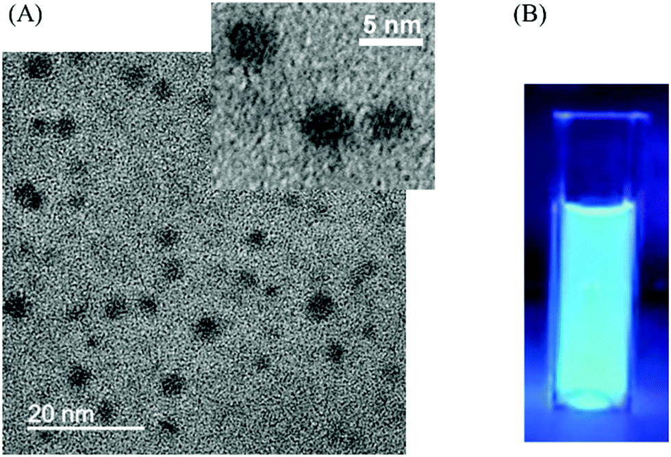 | ||
| Fig. 1 (A) TEM image of the CDs; (B) photograph of CDs in ethanol with 365 nm excitation. | ||
To investigate the photoelectric conversion behaviour, CDs were covalently linked to an indium tin oxide (ITO) surface through a 3-glycidoxypropyldimethoxymethylsilane (G-silane) monolayer based on the epoxy-amine reaction as shown in Fig. 2(A).19 An epoxy terminated monolayer on ITO was formed by silanization. Then, CDs from chitosan containing alkyl amine groups were covalently attached to the epoxy groups. After binding of CDs, the colourless ITO–silane surface became evenly light brown. As shown in Fig. S6 (ESI†), the absorbance of the ITO–silane–CDs surface at wavelengths <400 nm in the UV/Vis absorption spectrum increased compared to the ITO–silane surface, which indicated the binding of CDs to the ITO–silane surface. The X-ray photoelectron spectroscopy (XPS) survey spectrum in Fig. 2(B) confirms the linking of G-silane and CDs by the appearance of a nitrogen peak at 399.5 eV (Fig. S7(D), ESI†) assigned to the amine in the CDs from chitosan and the increase in the carbon signal. The Si 2p peak at 101.2 eV (Fig. S7(C), ESI†) was assigned to the organic Si in silane and corresponded to G-silane bonded to the ITO surface. The C 1s peak at 285.6 eV on the ITO–silane–CDs surface (Fig. S7(B), ESI†) was assigned to C–N bonds, and its absence on the ITO–silane surface (Fig. S7(A), ESI†) further confirmed the binding of CDs onto the ITO–silane surface. Atomic Force Microscopy (AFM) was used to image the ITO–silane and ITO–silane–CD surface. The height variation changed from 1.0 nm of ITO–silane to 2.0–4.5 nm of ITO–silane–CDs (Fig. S8, ESI†), which proved that CDs were homogenously coated onto the ITO–silane surface. The ITO–silane–CD surface was used for the investigation of photoelectrochemical responses.
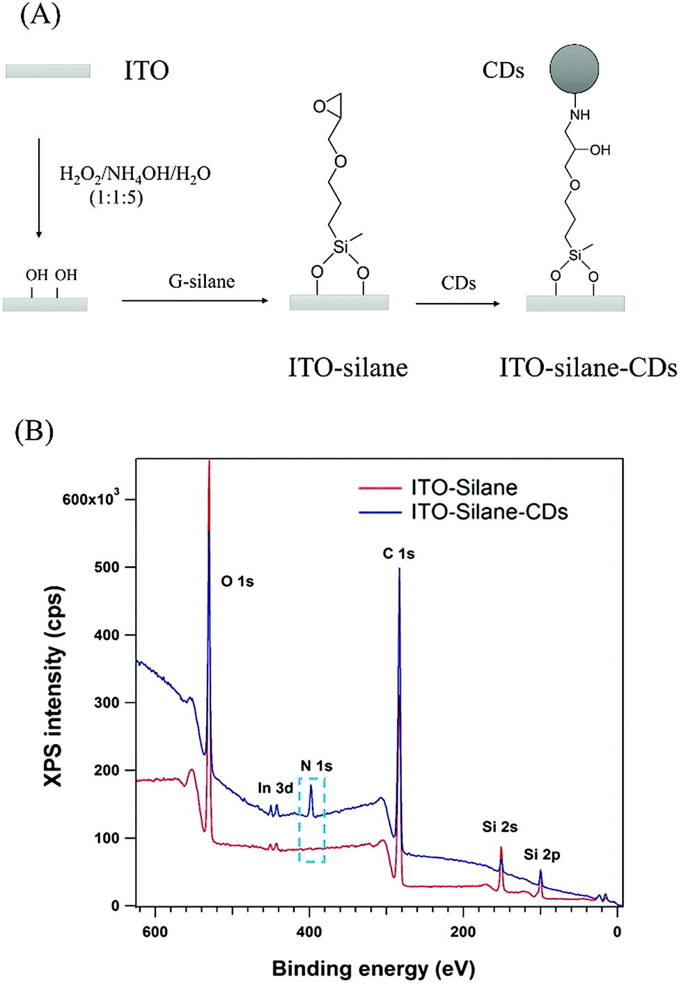 | ||
| Fig. 2 (A) Scheme of CDs binding onto ITO via a reaction with 3-glycidoxypropyldimethoxymethylsilane; (B) XPS full scan spectrum of the ITO–silane and ITO–silane–CDs. | ||
Photoelectric response measurements of ITO–silane–CDs were carried out by linear sweep voltammetry (LSV) from −0.6 to 1 V with a 5 mV s−1 scan rate in 10 mM pH 7.4 phosphate buffer with 0.1 M KCl in an electrochemical cell consisting of a platinum electrode and an Ag/AgCl electrode as the counter and reference electrodes, respectively. To prevent the interference of the ITO substrate under UV illumination, an adjustable diode laser (wavelength 400–450 nm, max 500 mW) with a UV filter that blocked the light of wavelengths lower than 420 nm was used as the chopped back side illumination source. The CDs could be excited by the 420–450 nm wavelength light (also see the fluorescence spectra of CDs in Fig. S3, ESI†). The light intensity was measured as 10 mW cm−2 with a calibrated power meter. As shown in Fig. 3(A), the ITO–silane–CDs surface showed an obvious photocurrent at anodic potentials with chopped illumination compared to the background dark current. The photocurrent under illumination appeared from 0.25 V and increased with the applied potential. Fig. 3(B) shows the LSV curves of ITO, ITO–silane, and ITO–silane–CDs surfaces from 0.2 V to 1 V under chopped illumination. The dark current of the ITO–silane–CD surface slowly increased at anodic potentials compared to the ITO and ITO–silane surfaces, suggesting that the CDs increased the conductivity of the surface. The photocurrent response of the ITO–silane–CD surface was significantly higher than that of ITO and ITO–silane surfaces. At 0.96 V, photocurrents (Iillumination− Idark) of ITO, ITO–silane, and ITO–silane–CD surfaces were 0.6 ± 0.1 μA cm−2, 1.2 ± 0.1 μA cm−2, and 2.8 ± 0.6 μA cm−2, respectively. The results confirmed the direct photoelectrochemical response of CDs derived from chitosan under 420–450 nm laser illumination. Fig. S9 (ESI†) shows the stability of the photocurrent of the ITO–silane–CD surface at 1.0 V with chopped illumination in 10 minutes. After 10 cycles, the photocurrent decayed to 68.4%. In this work, the photocurrent (Iillumination − Idark) of the ITO–silane–CD surface was 0.35 ± 0.02 μA cm−2 at 0.25 V, which is comparable to the reported performance of a covalently bound CdS quantum dot monolayer.15
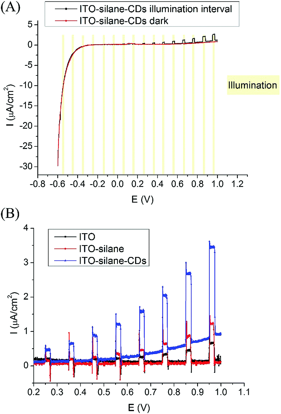 | ||
| Fig. 3 (A) LSV curves of ITO–silane–CDs in the dark and with chopped illumination (420–450 nm, 10 mW cm−2, a UV blocking filter was used to block light at wavelengths <420 nm); (B) LSV curves of ITO, ITO–silane, and ITO–silane–CDs with chopped illumination. | ||
We demonstrate here that solvothermally synthesized nitrogen doped CDs from chitosan have an n-type semiconductor-like photoelectrochemical behaviour. To better understand the mechanism for the photoelectrochemical response of the CDs, we used photoelectron spectroscopy in air to measure the ionization potential of CDs in powder form (Fig. S10, ESI†). We measured a value for the ionization potential of 5.52 ± 0.01 eV, corresponding to the energy of highest occupied electronic state of CDs. This is significantly larger than the ionization potential of other carbon systems such as graphite (∼4.45 eV)20 and graphene (4.5–5.1 eV).21–23 One reason for this might be nitrogen doping coming from the amine groups in the chitosan starting material. Nitrogen doping is commonly reported to reduce the work function of carbon systems,24–26 but it can increase the work function of graphitic systems if the incorporation of nitrogen atoms is at pyrrolic or pyridinic sites.27 We note that our XPS N 1s spectra do indicate both pyridinic and pyrrolic species in the CDs. Previous studies of nitrogen-doped CDs have reported large ionization potentials (6.16 eV),28 as in our case. We also note that the partial oxidation of the CDs may also increase the ionization potential as is the case for graphene oxide.29 The Tauc plot (Fig. S2(B), ESI†) derived from the UV/Vis absorption spectrum of CDs indicates an energy gap (Egap) of 3.7 eV, therefore putting the energy of the lowest unoccupied states at 1.8 eV. The excitation-dependent photoluminescence (PL) of CDs (Fig. S3, ESI†) indicates individual energy states (due to surface defects, functional groups, impurities, etc.) of CDs,30 which allows a very broad excitation band extending up to 500 nm (2.48 eV). The possibility of excitations significantly below the energy gap (3.7 eV) indicates a significant number of inter-gap states as shown in Fig. 4. There is a large energetic driving force for electron transfer to the ITO (Fermi energy, Ef ≈ 4.6 eV). At anodic potentials, the holes in CDs accept electrons from an electron donor (D) in electrolyte solution, which is OH− in this case. The formation of D+ from D using CDs as photocatalysts under illumination generates the photocurrent. The photocurrents of CDs related to their quantum yields were investigated. CDs with a higher quantum yields (QY) of 10.4% were synthesised by a one-step solvothermal carbonization of chitosan and ethylenediamine to increase the N content in the CDs. The ITO–silane–CDs with 10.4% QY showed higher photocurrents than those with 5.7% QY under the same binding and measurement conditions (Fig. S11, ESI†). This indicates that N doping plays an important role in the PL/QY and photocurrent response of CDs.
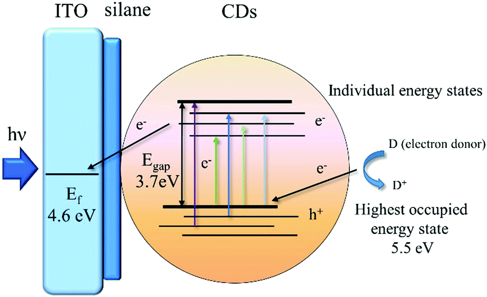 | ||
| Fig. 4 The mechanism of photoelectric conversion of CDs. | ||
The ITO–silane–CD surface was applied to ac-photocurrent imaging using the same experimental techniques usually applied to light-addressable potentiometric sensors (LAPS) and scanning photo-induced impedance microscopy (SPIM), which measure the local photocurrent by illuminating a semiconductor substrate with a focused, modulated laser beam. 2D images were obtained by moving the sensor in the XY plane with respect to the laser beam while recording the photocurrent, providing local electrochemical information such as impedance,31 ion concentrations,32 and surface charge.33 An array of poly(methyl methacrylate) (PMMA) dots was deposited onto the surface by a PDMS stamp using microcontact printing (μCP). Fig. 5(A) shows the circular islands of PMMA with a diameter of 40 μm and 30 μm gaps. Fig. 5(B) shows the corresponding ac-photocurrent image measured at a bias voltage of 1.8 V and a modulation frequency of 10 Hz with a focused 420–450 nm laser beam. The polymer dot array is clearly visible as a reduction in photocurrent because of the high impedance of PMMA. An ITO–silane surface without CDs, but patterned with PMMA dots was imaged with ac-photocurrent imaging as the control experiment. The control image (Fig. 5(D)) did not show any contrast, proving that contrast in the ac-photocurrent images comes directly from the photoelectrochemical response of CDs. To demonstrate the uniformity of the ITO–silane–CD surface, a small area (40 × 40 μm) ac-photocurrent scan with a step size of 0.4 μm at 1.8 V was performed. The ac-photocurrent image (Fig. S12, ESI†) proved that the surface was uniform and CDs were homogenously coated. As shown in Fig. S13 (ESI†), the ac-photocurrent remained stable for 15 min at a bias voltage of 1.8 V and a modulation of 10 Hz with unfocused 420–450 nm laser illumination.
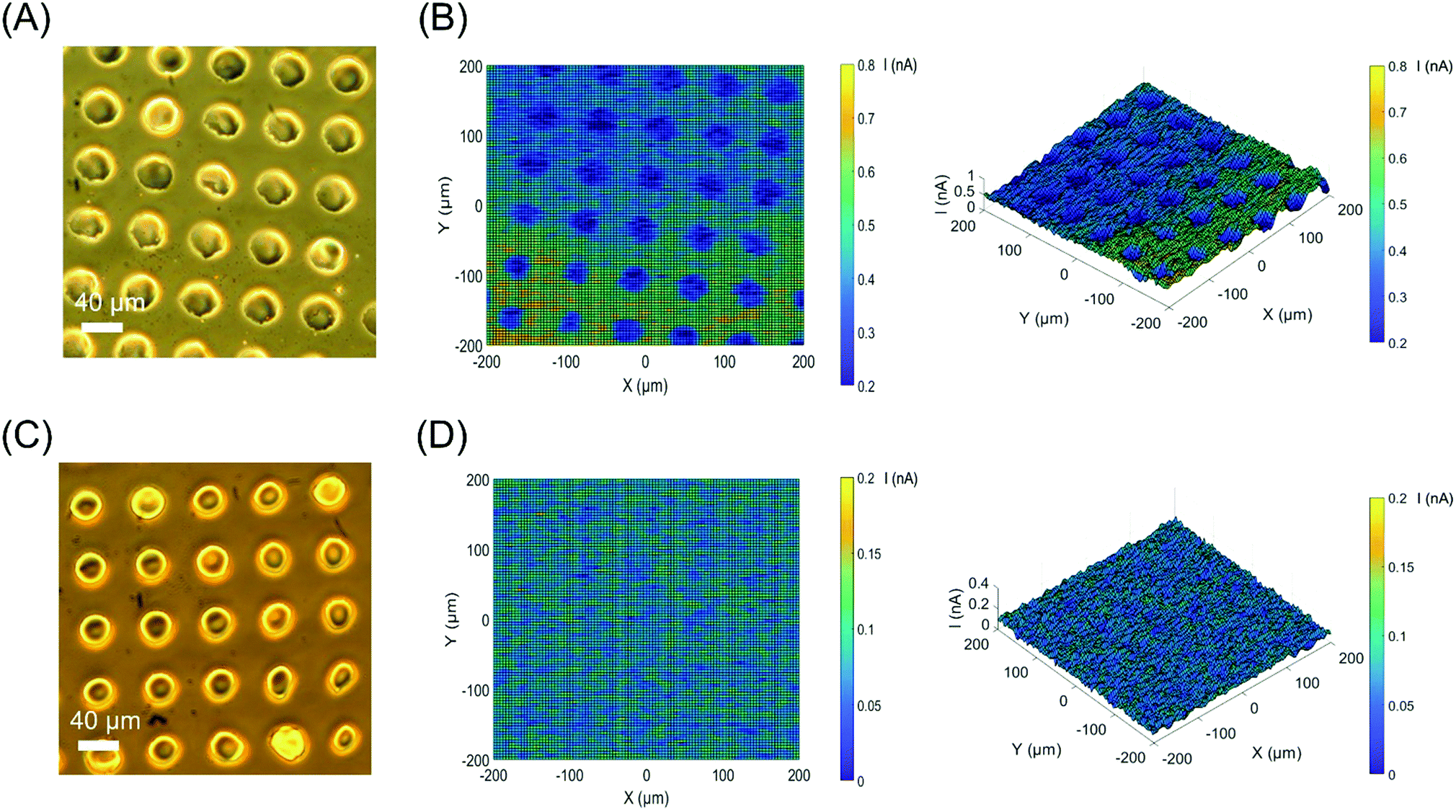 | ||
| Fig. 5 (A) Optical micrograph of a PMMA dot array on the ITO–silane–CD surface obtained by microcontact printing; (B) the corresponding ac-photocurrent image of (A) measured at 1.8 V; (C) the optical micrograph of a PMMA dot array on the ITO–silane surface; (D) the corresponding ac-photocurrent image of (C) measured at 1.8 V. | ||
To demonstrate the feasibility of using the CD modified ITO surface for bioanalytical and bioimaging applications, a multilayer of yeast cells was immobilized on the ITO–silane–CD surface by low gelling temperature agarose gel (Fig. S14(A), ESI†). Fig S14(B) (ESI†) shows the corresponding ac-photocurrent image at 1.5 V and 10 Hz. The yeast-agarose gel is visible as a reduction in the photocurrent because of the impedance and negative surface charge of yeast cells in pH 7.4 PBS solution.34 The control image of pure agarose gel (Fig. S14(D), ESI†) did not show any photocurrent contrast, proving that the signal came from the surface attached yeast cells.
Conclusions
In conclusion, CDs from chitosan were covalently linked to an ITO surface and showed a direct photoelectrochemical response. The photocurrent generated by CDs and the mechanism have been studied. The photocurrent was attributed to the enhanced electron-transfer process catalyzed by CDs under illumination. A homogeneous monolayer of CDs was successfully used for ac-photocurrent imaging. This opens up new applications for CDs as biocompatible, light-addressable electrochemical sensors in bioanalytical and bioimaging applications. As for well-established photocurrent imaging techniques such as LAPS and SPIM, a CD modified surface could be used for electrochemical imaging in the cell-surface attachment area, which is not accessible to other electrochemical or electrophysiological techniques. However, in contrast to LAPS and SPIM, which are limited to the measurement of ion concentrations35 or impedance,34 a CD modified surface could image a much broader range of parameters as carbon has been used as a common electrode material for the amperometric detection of metabolites and lends itself to standard immobilization techniques for enzymes and other electroactive molecules. The lateral resolution of ac-photocurrent imaging with a CD modified surface would only be limited by the quality of the focus of the light as there would be no lateral diffusion of photogenerated charge carriers as in the bulk semiconductors traditionally employed for LAPS and SPIM.36Author contributions
D.-W. Z., M.-M. T., and S. K. designed the experimental program and coordinated the project. N. P., H. L., H. G., and A. S. produced the CD samples and performed characterization of CDs. D.-W. Z. and N. M. D. performed the binding of CDs onto the ITO surface and photocurrent measurements. L. C. T. performed XPS measurements and analysis. T. D. performed AFM measurements and analysis. P. S. and O. F. performed PESA measurements and provided the mechanism. D.-W. Z. performed the μCP and ac photocurrent imaging. All authors contributed to the interpretation of the results. D.-W. Z., O. F., M.-M. T., and S. K. wrote the paper.Conflicts of interest
There are no conflicts of interest to declare.Acknowledgements
The authors are grateful to the EU for providing a Marie Skłodowska-Curie Individual Fellowship (H2020-MSCA-IF-2014-660489), to BBSRC (BB/P026788/1) and to EPSRC (EP/R021554/1). OF is a Royal Society University Research Fellow. PS acknowledges financial support from the Agence Nationale de la Recherche through the Labex projects CSC (ANR-10-LABX-0026 CSC) within the Investissement d’avenir program (ANR-10-120 IDEX-0002-02), by the International Center for Frontier Research in Chemistry (icFRC).References
- H. Yu, R. Shi, Y. Zhao, G. I. N. Waterhouse, L.-Z. Wu, C.-H. Tung and T. Zhang, Adv. Mater., 2016, 28, 9454–9477 CrossRef CAS PubMed.
- K. A. S. Fernando, S. Sahu, Y. Liu, W. K. Lewis, E. A. Guliants, A. Jafariyan, P. Wang, C. E. Bunker and Y.-P. Sun, ACS Appl. Mater. Interfaces, 2015, 7, 8363–8376 CAS.
- J. Bian, C. Huang, L. Wang, T. Hung, W. A. Daoud and R. Zhang, ACS Appl. Mater. Interfaces, 2014, 6, 4883–4890 CAS.
- H. Yu, H. Zhang, H. Huang, Y. Liu, H. Li, H. Ming and Z. Kang, New J. Chem., 2012, 36, 1031–1035 RSC.
- X. Zhang, F. Wang, H. Huang, H. Li, X. Han, Y. Liu and Z. Kang, Nanoscale, 2013, 5, 2274–2278 RSC.
- H. Yu, Y. Zhao, C. Zhou, L. Shang, Y. Peng, Y. Cao, L.-Z. Wu, C.-H. Tung and T. Zhang, J. Mater. Chem. A, 2014, 2, 3344–3351 CAS.
- K. D. Yang, Y. Ha, U. Sim, J. An, C. W. Lee, K. Jin, Y. Kim, J. Park, J. S. Hong, J. H. Lee, H.-E. Lee, H.-Y. Jeong, H. Kim and K. T. Nam, Adv. Funct. Mater., 2016, 26, 233–242 CrossRef CAS.
- L. Cao, S. Sahu, P. Anilkumar, C. E. Bunker, J. Xu, K. A. S. Fernando, P. Wang, E. A. Guliants, K. N. Tackett and Y.-P. Sun, J. Am. Chem. Soc., 2011, 133, 4754–4757 CrossRef CAS PubMed.
- R. Liu, H. Huang, H. Li, Y. Liu, J. Zhong, Y. Li, S. Zhang and Z. Kang, ACS Catalysis, 2014, 4, 328–336 Search PubMed.
- A. Ciesielski, S. Haar, A. Aliprandi, M. El Garah, G. Tregnago, G. F. Cotella, M. El Gemayel, F. Richard, H. Sun, F. Cacialli, F. Bonaccorso and P. Samorì, ACS Nano, 2016, 10, 10768–10777 CrossRef CAS PubMed.
- J. Shen, Y. Zhu, X. Yang, J. Zong, J. Zhang and C. Li, New J. Chem., 2012, 36, 97–101 RSC.
- S. K. Lai, C. M. Luk, L. Tang, K. S. Teng and S. P. Lau, Nanoscale, 2015, 7, 5338–5343 RSC.
- C.-B. Ma, Z.-T. Zhu, H.-X. Wang, X. Huang, X. Zhang, X. Qi, H.-L. Zhang, Y. Zhu, X. Deng, Y. Peng, Y. Han and H. Zhang, Nanoscale, 2015, 7, 10162–10169 RSC.
- T.-F. Yeh, C.-Y. Teng, S.-J. Chen and H. Teng, Adv. Mater., 2014, 26, 3297–3303 CrossRef CAS PubMed.
- W. Khalid, M. El Helou, T. Murböck, Z. Yue, J.-M. Montenegro, K. Schubert, G. Göbel, F. Lisdat, G. Witte and W. J. Parak, ACS Nano, 2011, 5, 9870–9876 CrossRef CAS PubMed.
- J. Briscoe, A. Marinovic, M. Sevilla, S. Dunn and M. Titirici, Angew. Chem., Int. Ed., 2015, 54, 4463–4468 CrossRef CAS PubMed.
- Z. Q. Li, C. J. Lu, Z. P. Xia, Y. Zhou and Z. Luo, Carbon, 2007, 45, 1686–1695 CrossRef CAS.
- S. Zhu, Q. Meng, L. Wang, J. Zhang, Y. Song, H. Jin, K. Zhang, H. Sun, H. Wang and B. Yang, Angew. Chem., Int. Ed., 2013, 52, 3953–3957 CrossRef CAS PubMed.
- M. Barreiros dos Santos, S. Azevedo, J. P. Agusil, B. Prieto-Simón, C. Sporer, E. Torrents, A. Juárez, V. Teixeira and J. Samitier, Bioelectrochemistry, 2015, 101, 146–152 CrossRef CAS PubMed.
- W. N. Hansen and G. J. Hansen, Surf. Sci., 2001, 481, 172–184 CrossRef CAS.
- S. M. Song, J. K. Park, O. J. Sul and B. J. Cho, Nano Lett., 2012, 12, 3887–3892 CrossRef CAS PubMed.
- Y.-J. Yu, Y. Zhao, S. Ryu, L. E. Brus, K. S. Kim and P. Kim, Nano Lett., 2009, 9, 3430–3434 CrossRef CAS PubMed.
- G. Giovannetti, P. A. Khomyakov, G. Brocks, V. M. Karpan, J. van den Brink and P. J. Kelly, Phys. Rev. Lett., 2008, 101, 026803 CrossRef CAS PubMed.
- D. H. Lee, J. A. Lee, W. J. Lee and S. O. Kim, Small, 2011, 7, 95–100 CrossRef CAS PubMed.
- J. O. Hwang, J. S. Park, D. S. Choi, J. Y. Kim, S. H. Lee, K. E. Lee, Y.-H. Kim, M. H. Song, S. Yoo and S. O. Kim, ACS Nano, 2012, 6, 159–167 CrossRef CAS PubMed.
- D. G. Kvashnin, P. B. Sorokin, J. W. Brüning and L. A. Chernozatonskii, Appl. Phys. Lett., 2013, 102, 183112 CrossRef.
- K. Akada, T.-o. Terasawa, G. Imamura, S. Obata and K. Saiki, Appl. Phys. Lett., 2014, 104, 131602 CrossRef.
- Y. R. Park, H. Y. Jeong, Y. S. Seo, W. K. Choi and Y. J. Hong, Sci. Rep., 2017, 7, 13 CrossRef PubMed.
- F. Zheng, W.-L. Xu, H.-D. Jin, X.-T. Hao and K. P. Ghiggino, RSC Adv., 2015, 5, 89515–89520 RSC.
- A. Cayuela, M. L. Soriano, C. Carrillo-Carrion and M. Valcarcel, Chem. Commun., 2016, 52, 1311–1326 RSC.
- D.-W. Zhang, F. Wu and S. Krause, Anal. Chem., 2017, 89, 8129–8133 CrossRef CAS PubMed.
- T. Yoshinobu, K.-i. Miyamoto, T. Wagner and M. J. Schöning, Sens. Actuators, B, 2015, 207(Part B), 926–932 CrossRef CAS.
- J. Wang, Y. Zhou, M. Watkinson, J. Gautrot and S. Krause, Sens. Actuators, B, 2015, 209, 230–236 CrossRef CAS.
- D.-W. Zhang, F. Wu, J. Wang, M. Watkinson and S. Krause, Electrochem. Commun., 2016, 72, 41–45 CrossRef CAS.
- K. Miyamoto and T. Yoshinobu, Sens. Mater., 2016, 28, 1091–1104 Search PubMed.
- Y. Guo, K.-i. Miyamoto, T. Wagner, M. J. Schöning and T. Yoshinobu, Sens. Actuators, B, 2014, 204, 659–665 CrossRef CAS.
Footnote |
| † Electronic supplementary information (ESI) available. See DOI: 10.1039/c7mh00784a |
| This journal is © The Royal Society of Chemistry 2018 |