
 Open Access Article
 This Open Access Article is licensed under a
 Creative Commons Attribution 3.0 Unported Licence
How the formation of interfacial charge causes hysteresis in perovskite solar cells†
Stefan A. L.
Weber
 *ab,
Ilka M.
Hermes
a,
Silver-Hamill
Turren-Cruz
c,
Christopher
Gort
a,
Victor W.
Bergmann
a,
Laurent
Gilson
a,
Anders
Hagfeldt
c,
Michael
Graetzel
d,
Wolfgang
Tress
c and
Rüdiger
Berger
a
*ab,
Ilka M.
Hermes
a,
Silver-Hamill
Turren-Cruz
c,
Christopher
Gort
a,
Victor W.
Bergmann
a,
Laurent
Gilson
a,
Anders
Hagfeldt
c,
Michael
Graetzel
d,
Wolfgang
Tress
c and
Rüdiger
Berger
a
aMPI for Polymer Research, Ackermannweg 10, 55128 Mainz, Germany. E-mail: Stefan.Weber@mpip-mainz.mpg.de
bJohannes Gutenberg University, Department of Physics, Staudingerweg 10, 55128 Mainz, Germany
cLaboratory of Photomolecular Science, Institute of Chemical Sciences and Engineering, École Polytechnique Fédérale de Lausanne, 1015 Lausanne, Switzerland
dLaboratory of Photonics and Interfaces (LPI), Institute of Chemical Sciences and Engineering, École Polytechnique Fédérale de Lausanne, 1015 Lausanne, Switzerland
First published on 5th June 2018
Abstract
In this study, we discuss the underlying mechanism of the current–voltage hysteresis in a hybrid lead-halide perovskite solar cell. We have developed a method based on Kelvin probe force microscopy that enables mapping charge redistribution in an operating device upon a voltage- or light pulse with sub-millisecond resolution. We observed the formation of a localized interfacial charge at the anode interface, which screened most of the electric field in the cell. The formation of this charge happened within 10 ms after applying a forward voltage to the device. After switching off the forward voltage, however, these interfacial charges were stable for over 500 ms and created a reverse electric field in the cell. This reverse electric field directly explains higher photocurrents during reverse bias scans by electric field-assisted charge carrier extraction. Although we found evidence for the presence of mobile ions in the perovskite layer during the voltage pulse, the corresponding ionic field contributed only less than 10% to the screening. Our observation of a time-dependent ion concentration in the perovskite layer suggests that iodide ions adsorbed and became neutralized at the hole-selective spiro-OMeTAD electrode. We thereby show that instead of the slow migration of mobile ions, the formation and the release of interfacial charges is the dominating factor for current–voltage hysteresis.
Broader contextPerovskite solar cells have electrified the solar cell research community with astonishing performance and surprising material properties. Very efficient (>20%) devices with perovskite layers of low defect density can be prepared by cheap and simple solution-based processes at moderate temperatures (<150 °C). For commercializing this technology, a stable and reliable operation is required. In perovskite solar cells, however, the output power strongly depends on the history of the device in terms of bias voltage (causing hysteresis) or illumination (known as light soaking effect). The underlying process is connected to the migration of ionic charges within the perovskite layer. In our study, we were able to map and follow the vertical charge distribution in the perovskite layer of an operating device. In particular, we found that thin layers of localized charge were forming at the electrode interfaces when we changed the external voltage or illuminated the device. Our results show that the formation and release of these ionic interface charges determine the time scales for current–voltage hysteresis in perovskite solar cells. Our study demonstrates that a precise control over the interfaces in perovskite solar cells is the key for controlling and suppressing hysteresis in perovskite solar cells. |
Introduction
Herein we report on experiments to visualize local charge re-distribution in lead halide perovskites that are responsible for current–voltage hysteresis. We found that interface charges localized at the electron-selective contact generated an electric field that modified the charge extraction in the device. Thus, the formation and release of these ionic interface charges instead of a slow ionic charge transport determine the time scales for current–voltage hysteresis in perovskite solar cells.Recently, consensus has been reached that current density–voltage (J–V) hysteresis in perovskite solar cells is connected to ion migration in the perovskite layer.1 In this picture, space charge layers of mobile ions at the electrodes shield the electric field in the perovskite layer on timescales of milliseconds to seconds.2 Such a screening of the electric field in the perovskite layer has been observed both at short- and open circuit conditions.3,4 This modification of the internal electric field influences the charge extraction efficiency and recombination losses inside the perovskite layer and the photocurrent becomes dependent on the voltage scan direction.5,6 However, until now it is unclear if the timescales of the ion migration itself are the sole reason for the slow response of the electric field or if other factors such as interface dipoles7–9 or chemical reactions of ionic species at the interfaces10 play a role, too.
In the commonly used model that explains hysteresis by ion migration, the ionic species are evenly distributed and free to move throughout the entire perovskite film1,5,6,11,12 (Fig. 1a). Experimentally, the lateral migration of methylammonium and iodide species has been observed in perovskite films, proving that mobile ionic species exist.13–16 The exact mechanism of the migrating process and how it affects the charge extraction perpendicular to the perovskite film, however, remains unclear. In particular, it is still unclear (i) what the exact mechanism of migration is (hopping via vacancies or via interstitials17), (ii) where exactly the mobile ions are located (across the film or at grain boundaries or interfaces) and (iii) what the migration paths are (bulk transport15 or grain boundaries,18Fig. 1a and b).
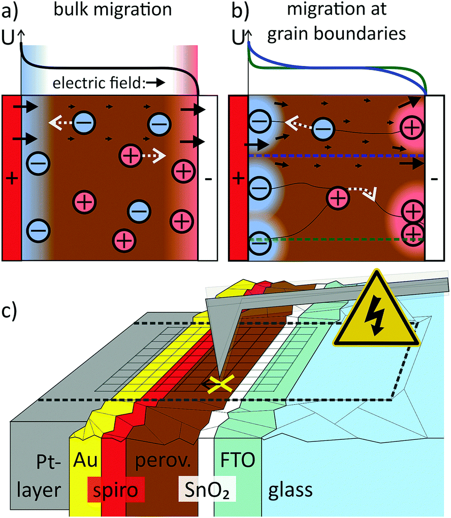 | ||
| Fig. 1 Illustration of potential (U), electric field (black arrows) and ion distribution for different migration paths for mobile ions: (a) if ions can migrate through the bulk of the perovskite layer, uniform electrostatic double layers (EDLs) will form at either electrode that screen the external device potential. (b) If ions migrate preferentially at grain boundaries, the EDLs and the electric field distribution will be heterogeneous. (c) In time-resolved KPFM, the CPD response to a voltage- or light-pulse is recorded in a pointwise spectroscopy approach subsequently at different positions on the sample. | ||
The simple bulk ion migration model is not sufficient to explain the observation that the incorporation of a suitable material in the electron transport layer (ETL), such as mesoporous TiO2,19 PCBM20–23 or SnO2,24 in perovskite solar cells results in almost hysteresis-free devices. In the case of SnO2, the reduction in hysteresis was attributed to a more efficient electron extraction, reducing recombination losses.24 In the case of PCBM, the ion migration was suggested to be suppressed by passivating interfacial defects.25 The strong influence of the ETL material demonstrates the crucial role of interfaces for hysteresis. Nevertheless, the exact interplay between ion migration and interface effects remains unexplored. In order to solve the puzzle, methods that can map the spatial and temporal evolution of the electric field in the device are required.
We developed such a time-resolved method based on Kelvin probe force microscopy (KPFM)3,4,26–31 by decoupling the spatial mapping and the recording of the temporal evolution of the local contact potential difference (CPD). Thereby, we achieved sub-ms KPFM time resolution (Fig. 1c and Methods section). We used this time-resolved (tr-)KPFM to follow the charge re-distribution in a hysteretic methylammonium/formamidinium lead iodide/bromide perovskite solar cell device (details on the composition in the Methods section) upon applying an external voltage or a light pulse. We found that the electric field across the perovskite layer was screened via a combination of localized positive interface charge at the ETL and a negative ionic space charge across the entire perovskite layer. Our experiments demonstrate, that the electric field generated by the surface charge was the dominating factor for screening electric fields in the perovskite layer.
Results
Dynamics with pulsed voltage
For our study, we chose a perovskite solar cell with particularly pronounced hysteresis, as we expected to observe significant effects of internal charge re-arrangement in such a device. To gain access to the cross section, the device was cleaved and a 50 μm wide region was polished with a focused ion beam procedure (see also Methods and ref. 3 and 26). The procedure only had minor influence on the performance and the hysteresis in the device, with efficiencies of 12.2% (upward scan) and 16.5% (downward scan, Fig. 2a, and Fig. S2, ESI†). On the cross section, we identified the different layers of the perovskite solar cell from the scanning force microscopy (SFM) phase signal of the mechanical tip oscillation (Fig. 2b). For more clarity, we have marked the interfaces to the active perovskite layer in the phase image and in all following images with dashed lines. In the CPD map recorded before the voltage pulse, the potential in the perovskite layer was flat, i.e. a built-in potential, which might have been introduced by the difference of work functions of contact layers, was shielded by the internal charge distribution (Fig. 2c and Fig. S2, ESI†). This CPD distribution represents the equilibrium potential distribution that we refer to as the static CPD.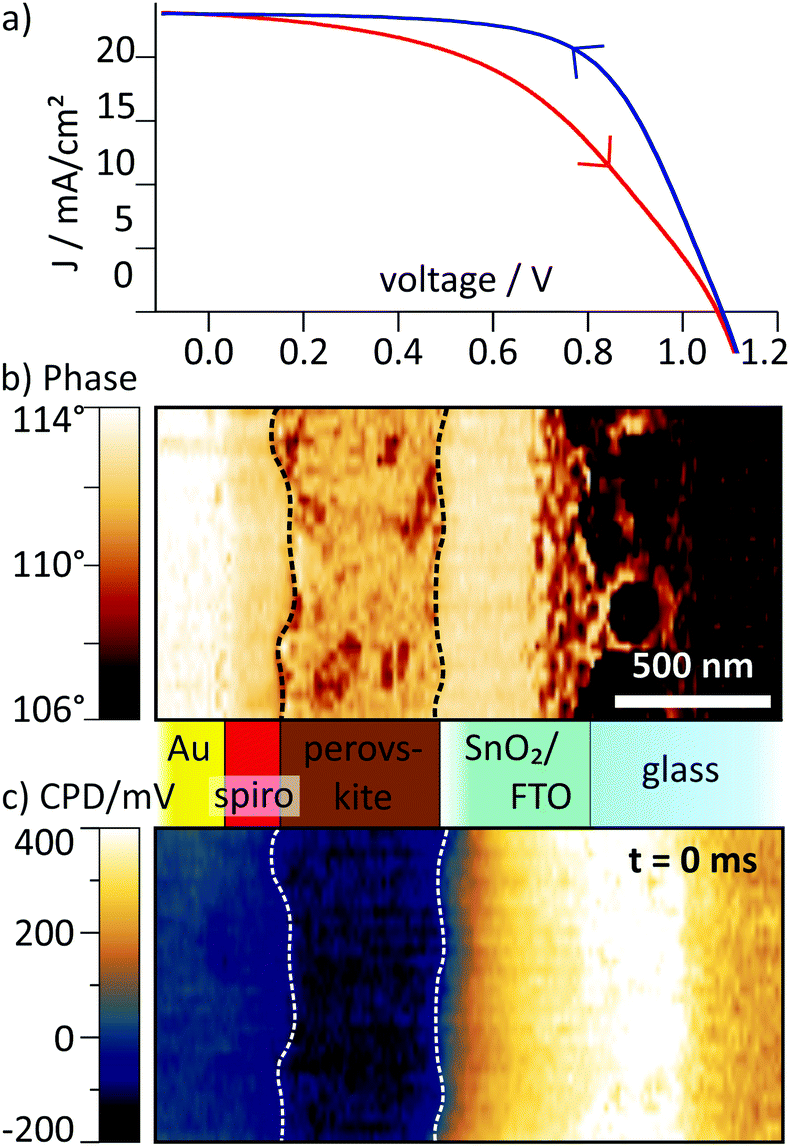 | ||
| Fig. 2 (a) Current density (J) vs. voltage (V) curves in forward (red) and reverse (blue) scan for the device under investigation. The curve was recorded after the focussed ion beam treatment with a voltage sweep rate of 130 mV s−1. (b) SFM phase map, recorded simultaneously with the CPD maps, showing the contrast between the different layers of the solar cell. From left to right the 80–90 nm thick gold electrode was followed by the spiro-OMeTAD hole transport layer, which had a thickness of 80–180 nm with a rough interface to the perovskite layer. The perovskite layer itself had a varying thickness of 300–550 nm with rough interfaces to both spiro-OMeTAD and SnO2/FTO. The 15 nm thick SnO2 electron transport layer was too thin to be visible in the phase map. (c) Map of the static CPD, i.e. the CPD distribution before the voltage pulse was applied. | ||
Using tr-KPFM, we were able to reconstruct CPD maps with a temporal resolution of 0.5 ms (see ESI† and Methods for more details). Movies generated from these KPFM snapshots are provided as ESI.† For the pulsed voltage experiments, we applied a 750 ms long voltage pulse of −0.5 V to the FTO electrode while the gold electrode was grounded. The voltage pulse simulates a forward (0 V → −0.5 V) and backward (−0.5 V → 0 V) voltage scan when applying a positive voltage to the gold cathode during a JV scan. To distinguish between transient and static charge distribution, we subtracted the static CPD (Fig. 2c) from the CPD maps at later times. These transient ΔCPD maps contain information about charge re-distribution dynamics caused by the external voltage pulse at a given time after applying the voltage pulse.
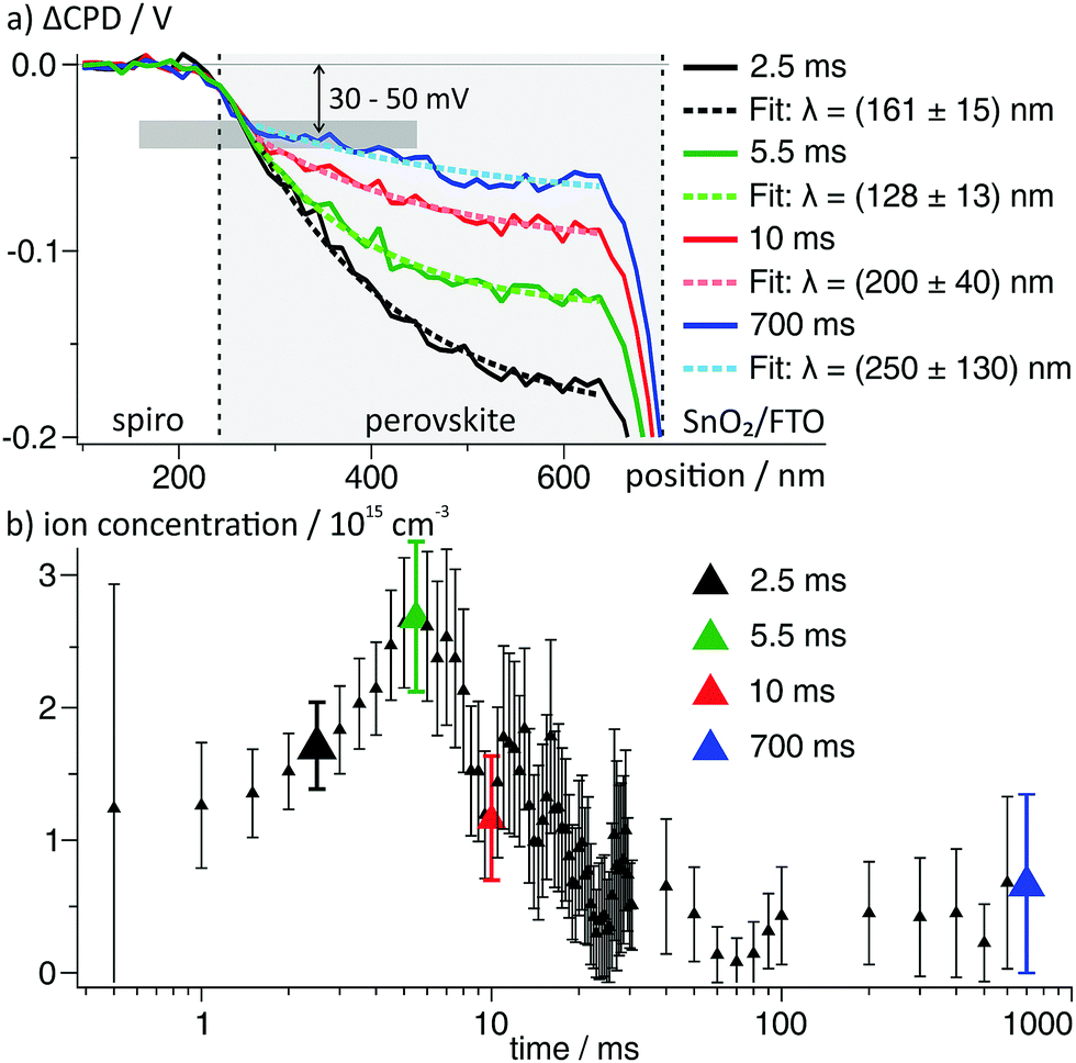
In the ΔCPD map, a potential gradient across the perovskite layer was present 2.5 ms after switching on the external voltage (Fig. 3a). The corresponding section graph of the potential distribution (black curve Fig. 3b) shows a strong asymmetry: at the spiro-OMeTAD/perovskite interface, the potential bends downwards, becoming flatter towards to perovskite/SnO2 interface. At the interface to the SnO2/FTO electrode, the ΔCPD drops by more than 200 mV within less than 100 nm. Section graphs from the same position recorded at 10 ms and 700 ms after the switching (red and blue curve in Fig. 3b) show that the magnitude of the potential decay across the perovskite layer decreased over time. Now, the majority of the potential (∼400 mV) drops at the perovskite/SnO2 interface, effectively screening the external potential from the perovskite layer. The sharp potential step at the perovskite/SnO2/FTO interface corresponds to a dipolar charge with positive charges on the perovskite side and negative charges on the SnO2/FTO side (red and blue shaded areas at the perovskite/SnO2 interface in Fig. 3b; see Methods section for a note on how to identify charges from the potential distribution).
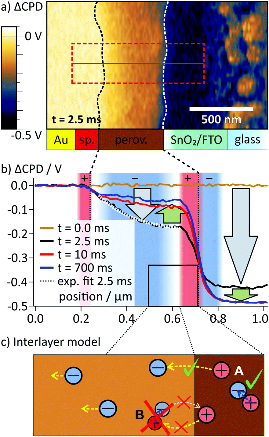 | ||
| Fig. 3 (a) ΔCPD map 2.5 ms after the switching, where a strong potential gradient is present inside the perovskite. The interfaces of the perovskite layer as obtained from the phase image in Fig. 2b are indicated with dashed lines (sp.: Spiro-OMeTAD). (b) Averaged ΔCPD sections from the rectangular area marked in a. During the first 2.5 ms both on the FTO and inside the perovskite layer the local potential decreased (gray arrows). Afterwards, the potential on the FTO electrode decreased and the potential in the perovskite layer increased (green arrows). The increase was caused by a slow screening of the internal electric field, mainly by positive interface charges at the perovskite/SnO2 interface that were compensated by electrons on the FTO side. Here, regions of positive charge (convex curvature) are shaded in red and negative regions (concave curvature) in blue. (c) To explain the asymmetry in the potential distribution, we propose that positive charges are localized at the perovskite/SnO2 interface. A possible scenario for localization is the formation of an interlayer with locally lower activation barrier for iodide/iodide vacancy formation. Thereby, the migration of iodide into the perovskite is possible (A), but the migration of vacancies is blocked (B). | ||
Comparing the CPD distributions for 10 ms and 700 ms shows that it took hundreds of milliseconds to reach an equilibrium potential distribution across the perovskite layer (Fig. 3b). Relaxation times on millisecond timescales have been attributed to the slow migration of ionic species inside the perovskite layer,2,5,6,32 suggesting ion migration as the underlying mechanism for the observed CPD dynamics. The dimensions of the imaging area were larger than the typical grain size of ∼100 nm for this solar cell type. Nevertheless, both potential distribution in the perovskite layer and the surface charge at the perovskite/SnO2 interface showed a homogeneous CPD contrast along the perovskite layer. A CPD contrast could be an indication for faster ion migration along grain boundaries,16,33 for example (Fig. 1b). The absence of a CPD contrast is therefore an indication of bulk ion transport (Fig. 1a).
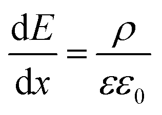
To quantify the charge at different positions in the cell, we calculated the charge carrier densities based on the one-dimensional Maxwell equation, that connects the electric field, E, with the charge carrier density, ρ:
 | (1) |
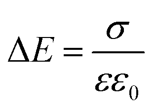 | (2) |
Inside the perovskite layer, the potential was exponentially decaying towards the FTO side with a decay length of (161 ± 15) nm, corresponding to a negative space charge density (dashed gray fit in Fig. 3b). We assume that this charge is caused by ionic space charge. To estimate the ion concentration, we assume that the mobile ions in the perovskite form an electrostatic double layer (EDL) towards the spiro-OMeTAD interface, similar to a solid-state electrolyte.6,11,32 The screening length of the EDL in an electrolyte with charge carrier concentration c and dielectric permittivity ε can be estimated by the Debye screening length:36
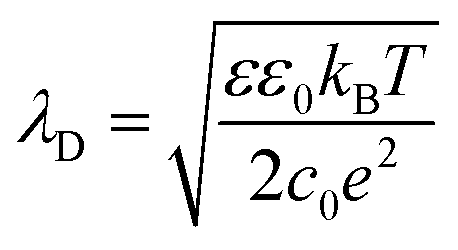 | (3) |
Using our results, the total ionic charge in a ∼400 nm thick perovskite layer is (1.1 ± 0.2) × 10−8 C cm−2. Thus, the amount of negative ionic charge in the perovskite layer only accounts for ∼10% of the localized positive charge at the perovskite/SnO2 interface. This discrepancy shows that additional processes happen that either increase the positive interface charge or that neutralize parts of the negative space charge.
The commonly used model for ion migration in perovskite solar cells assumes that mobile ions and ion vacancies are evenly distributed across the perovskite layer. Our observations of a purely negative diffuse space charge in the perovskite and highly localized positive surface charge at the perovskite/SnO2 interface clearly contradict this solid-state electrolyte model. Here, we would expect the EDLs to form on either side of the perovskite layer.5,6,32 Due to symmetry, the EDLs should – once equilibrated – generate potential steps of the same magnitude and with the same screening length at either side of the perovskite layer.11,32 However, what we observed here and in our previous KPFM cross section study3 is a strong potential drop at the perovskite/ETL interface and a much weaker potential screening towards the perovskite/HTL interface. This asymmetric screening indicates that different screening mechanisms act on both of these interfaces.
Richardson et al. have found an asymmetric potential distribution due to a complete depletion of the mobile ionic charge in a 100 nm wide region at one interface and a high concentration of ions at the other interface.12 In such a depletion region, the potential would deviate from the exponential behavior of an EDL. In our experiments, we did not observe such deviations over the duration of the voltage pulse (Fig. S3, ESI†).
As a model to explain the observed voltage transients and potential distributions, we suggest that free iodide/iodide-vacancy pairs are generated upon application of an electric field in a thin interlayer, thinner than the lateral KPFM resolution of 50 nm, close to the perovskite/SnO2 interface (Fig. 3c). The here generated iodide species are free to move across the entire perovskite layer, whereas the vacancies remain localized at the perovskite/SnO2 interface (A in Fig. 3c). The assumption of immobile positive ions is necessary to keep the positive charges localized at the perovskite/SnO2 interface. Here, we can only speculate about the physical reason for the formation of the interlayer: one scenario could be a field-induced destabilization of the perovskite crystal structure close to the interface. Thereby, the activation energy for the formation of an iodide defect could be locally lowered.17 Such spatial variations in the activation energies could also explain the differences in the ion densities between our estimation and the results and the literature,32,37 as macroscopic measurements cannot account for spatial variations in the activation energy. The interfacial iodide vacancies would be immobile because they cannot be filled by iodide from outside the surface region (B in Fig. 3c). In our model, iodide would therefore migrate via interstitial sites/Frenkel defects.
One explanation for the surplus of surface charge at the perovskite/ETL interface would be that this interlayer of destabilized perovskite is strongly polarizable, inducing the formation of a surface dipole (higher local ε). In this case, the polarization at the interface would be following almost instantaneously any change in the external voltage. To test if this is the case, we next analyzed the CPD dynamics after the voltage pulse.
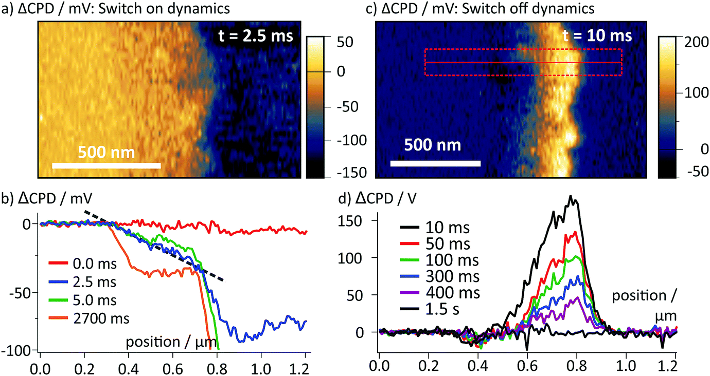
Upon switching off the external voltage, the ΔCPD jumped within 6 ms to a positive value inside the perovskite layer (Fig. 4a, t = 6 ms). The distribution of this overshoot voltage is again homogeneous along the perovskite layer and we did not observe strong fluctuations in the ΔCPD signal, e.g. caused by grain boundaries. The section graphs in Fig. 4b reveal that the ΔCPD increases linearly from the spiro-OMeTAD side towards the SnO2 side. During the voltage decay up to 500 ms after switching off the external voltage, the potential remained linear within the perovskite layer. Such a linear ΔCPD distribution corresponds to a homogenous electric field inside the perovskite layer with no space charges in between the electrodes. The electric field is generated by negative charges localized in a 50 nm wide region at the spiro-OMeTAD/perovskite interface and a dipolar surface charge in a 170 nm wide region at the perovskite/SnO2 interface, respectively (red and red/blue shaded areas in Fig. 4b).
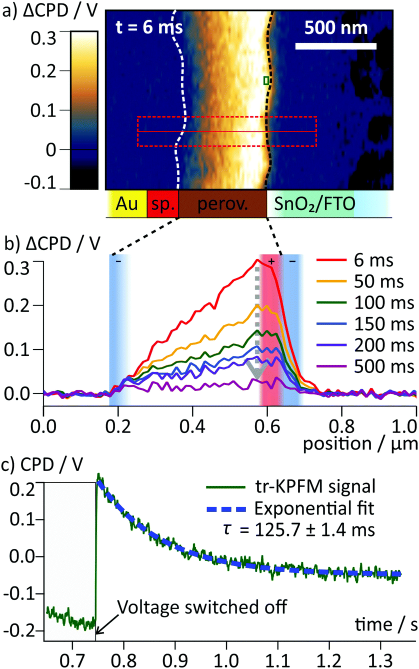 | ||
| Fig. 4 (a) Map of ΔCPD measured 6 ms after switching off the voltage. The interfaces of the perovskite layer are marked with dotted lines. (b) Averaged section graphs obtained from the region indicated by the red box in (a) at different times after the switching. Regions with non-linear ΔCPD profile correspond to non-zero local charge density and are indicated by red/blue shaded boxes according to the polarity of the charges. In the ΔCPD map recorded 500 ms after the switching, an additional vertical offset of 10 mV was observed (Fig. S3, ESI†). (c) tr-KPFM trace recorded at a position close to the perovskite/SnO2 interface indicated by a red box in (a), showing a voltage overshoot following the switching of the FTO voltage from −0.5 V to 0 V. The overshoot decay was fitted with a single exponential function. | ||
To follow the decay of the electric field over time, we analysed the ΔCPD maps over 500 ms after the voltage pulse (Fig. 4b). The section graphs show that although the magnitude of the positive ΔCPD decreased, the overall triangular shape of the section curve remained unchanged. Over the measurement time, the space charge regions remained confined in regions at the selective contacts. To obtain the timescale of the CPD decay after the switching, we analysed a local CPD transient curve recorded close to the perovskite/SnO2 interface. We fitted the decay with an exponential curve with a decay time of (125 ± 1.4) ms (Fig. 4c). This timescale for the surface charge relaxation is a factor of 40 slower compared to the formation time. This stabilization indicates that the surface charge does not simply originate from a region of increased polarizability. Rather, the charge is stabilized directly at the perovskite/SnO2 interface, e.g. by the molecular interface structure38 or chemical reactions.10,13 The absence of negative space charges in the perovskite layer suggests that the dynamics of the mobile ions are much faster than we could resolve in our measurements and thus play no role for the observed decay dynamics. This is a further confirmation for our earlier conclusion that the observed ion migration and the surface charge are two separate phenomena.
Model for hysteresis
The results on the dynamics of the internal electric field so far can directly explain the strong hysteresis in the investigated device: during the upward scan of the voltage, the electric field in the device drives electrons and holes to the opposite electrode and the extraction efficiency is lower (Fig. 5a and b). During the relaxation of the electric field in the perovskite, we propose that ions adsorb at the spiro-OMeTAD/perovskite interface and “freeze” the charge distribution (Fig. 5c). During the downward scan, the strong reverse field induced by the stabilized charge distribution supports the charge extraction and a higher photocurrent is measured (Fig. 5d). Next to the influence on the electronic drift, the presence of interfacial charges could also influence the charge extraction via energetic barriers or recombination at the interfaces.5,39,40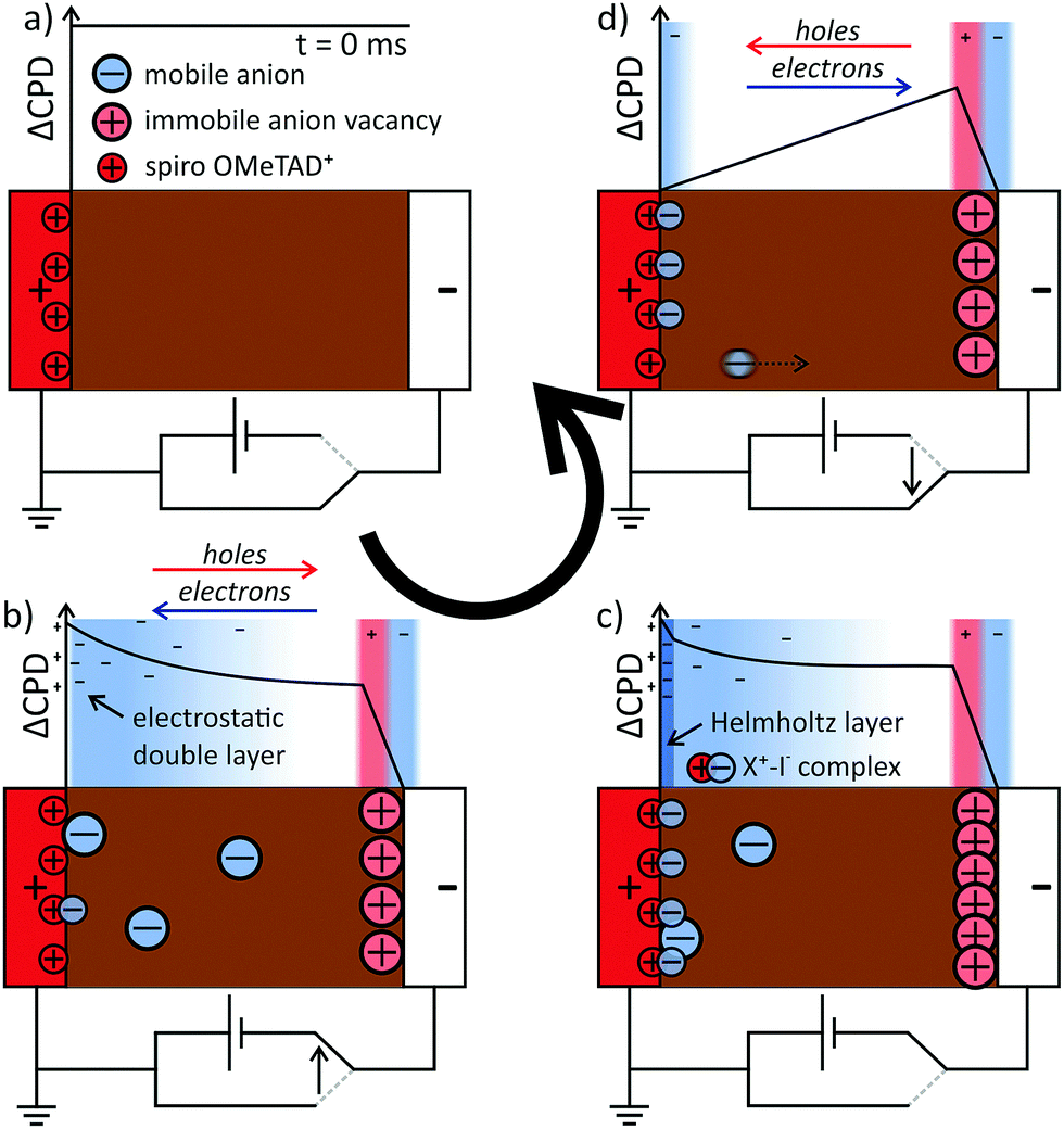 | ||
| Fig. 5 Proposed mechanism for hysteresis: (a) in equilibrium, the perovskite layer is field-free. (b) In the presence of an electric field across the cell, mobile iodide ions are released from the perovskite at the anode interface. The electric field drives electrons towards the cathode and holes towards the anode. The drifting ions start to screen the external voltage. Additionally, ions are adsorbed or form complexes at the cathode interface. (c) The adsorption/complexation and neutralization (X+–I−) at the cathode is depleting the perovskite from mobile ions. Positive charges at the anode interface are compensated by electrons from the FTO. These charges now screen almost the entire electric field and the potential is flat across the perovskite layer. (d) Upon switching off the field between the electrodes, the slow release of the separated charges at the interfaces keeps a reverse electric field in the perovskite layer. This reverse field aids in driving electrons towards the anode and holes towards the cathode. | ||
To search for a possible stabilization mechanism for the charge distribution after switching off the external voltage, we further analysed the dynamics of the negative space charges in the perovskite layer after switching on the voltage. Here, we found that the EDL decay lengths varied for different times after the voltage pulse. In particular, the decay length reached a minimum of (128 ± 13) nm at 5.5 ms and recovered to a value of ∼200 nm at 10 ms after switching on the voltage (Fig. 6a).
 | ||
| Fig. 6 (a) ΔCPD profiles in the perovskite layer from the area indicated by small box in Fig. 3. The dashed lines are single exponential fits to the data. All ΔCPD profiles overlap to a point ∼50 nm away from the spiro-OMeTAD and at a ΔCPD of −30 to −50 mV. (b) Calculated ion concentration from the decay lengths obtained from fitting 75 potential profiles at times from 500 μs to 700 ms viaeqn (3). The larger datapoints correspond to the curves depicted in (a) using the same color code. | ||
Naively, we could assign the variation in the screening length to a non-equilibrium ion distribution after a change in the electrode voltage. However, in numerical simulations of the ion dynamics upon a change in the applied voltage the screening length remained constant.41 We can therefore conclude that the observed ion distributions are in a quasi-equilibrium at all measuring times.
Using eqn (3), we again calculated the time-dependent ion concentration inside the perovskite layer from the measured screening length. Starting from a value of (1.2 ± 0.5) × 1015 cm−3 (0.5 ms), the charge density increased to (2.7 ± 0.6) × 1015 cm−3 at 5.5 ms after the switching, and decreased back to 0.3–1 × 1015 cm−3 within the following 10–20 ms (Fig. 6b). We observed that all potential curves overlap at a point ∼50 nm away from the spiro-OMeTAD layer (grey horizontal bar in Fig. 6a). The formation of a potential elbow in this point indicates a higher charge density, e.g. connected to the formation of a Helmholtz-layer of localized ions at the interface to the spiro-OMeTAD (Fig. 5c).
Contreras et al.42 have suggested that a specific interaction between the methylammonium cation and the TiO2 interface is responsible for slow (0.1–10 Hz) dynamics in perovskite solar cells. From impedance spectroscopy and bias-dependent capacitance measurements, they concluded that methylammonium cations accumulate at the TiO2 interface. Although we found an accumulation of positive charge at the anode interface, as well, our observation of a negative space charge in the perovskite together with the strong localization of the positive charge contradict this interpretation. Furthermore, Contreras et al. found reduced slow dynamics in mixed methylammonium/formammidinium (60/40) lead iodide devices. Our devices were made with a (1/5) methylammonium/formammidinium ratio, making a specific cation interactions of methylammonium as the sole reason for hysteresis unlikely.
Carrillo et al. have discussed possible chemical reactions of mobile iodide with TiO2 and spiro-OMeTAD in context of hysteresis and device degradation.10 They suggested that weak Ti–I–Pb bonds could “facilitate interfacial accommodation of moving iodide ions”. In this model, the release of iodide from the interfacial layer should be slower, as it is an endothermal process. However, we observed that the formation of positive charge at the anode interface (corresponding to the release of iodide) was much faster than the reverse process. Here, a reversible chemical reaction or complexation of the iodide with positively charged spiro-OMeTAD (Fig. 5c, also suggested by Carrillo et al.10) could explain both the observed time-dependent negative charge density and the asymmetry in the charge distribution with a surplus of positive charges at the perovskite/SnO2 interface. Nevertheless, hysteresis has been observed in devices without any hole transport layer,43 suggesting that the observed effects are not specific for spiro-OMeTAD. Recent KPFM results suggest that the position of this interface charge, i.e. anode or cathode interface, can be influenced by the composition of the perovskite, namely by the iodide excess in the precursor solution,4 suggesting that the interface charge is located within and influenced by the perovskite crystal.
Independent of the stabilization mechanism, the slow release of bound ions from the perovskite/hole transporter interface explains the slower relaxation dynamics upon switching off the external voltage. The strong electric field will make the ion transport across the perovskite layer very fast, explaining the absence of space charge (Fig. 5d).
Dynamics with pulsed illumination
To test if similar effects are present in an illuminated device, we performed experiments with light pulses generated by a white light source. The device was set to open circuit conditions with the gold cathode grounded and the FTO anode floating. This situation simulates the so-called light-soaking conditions when the device is illuminated under open circuit for a couple of minutes before recording a j–V curve. Upon switching on the light, the electrode potential on the FTO jumped to ∼−170 mV within ∼2 ms and slowly decreased over the following three seconds by another ∼150 mV (see ESI†).In the ΔCPD map 2.5 ms after the switching, we again found a strong interface charge at the perovskite/SnO2 interface. However, almost no potential gradient in the ∼400 nm thick perovskite layer could be observed (Fig. 7a). Only when averaging over entire ΔCPD map (Fig. 7b) we found a weak electric field of ∼870 V cm−1 over the perovskite layer. At later stages, the potential in the perovskite layer became flat again with a negative offset of 30–40 mV (orange curve in Fig. 7b), comparable to the offset that we observed in the experiments with pulsed voltage (Fig. 6a). Possible reasons for the observation of a much weaker electric field and the absence of curvature in the potential are the higher noise level due to intensity fluctuations in the light source or the relatively slow switching time of ∼10 ms of its mechanical shutter. Moreover, the screening of the field could be stronger due to a higher photo-induced ion concentration44 or due to photo-excited electronic carriers, although we would expect symmetric screening at both electrodes in this case. The observation of a ΔCPD offset within the perovskite layer at later times indicates that negative ionic charges accumulated at the spiro-OMeTAD/perovskite interface (Fig. 5c). The absence of an exponentially decaying potential in the perovskite layer indicates again that mobile ions play a minor role in the electric field screening compared to the perovskite/SnO2 interface charge.
 | ||
| Fig. 7 Tr-KPFM experiments with pulsed illumination. (a) ΔCPD map 2.5 ms after switching on the light (b) ΔCPD section graphs at different times obtained by averaging over the entire image range of the map in (a). The dashed line is a linear fit to the 2.5 ms section graph, showing that there is an electric field of ∼870 V cm−1 present in the perovskite layer. (c) ΔCPD map 10 ms after switching off the illumination. (d) Averaged section graph from the area marked in (c), revealing similar dynamics as in the pulsed voltage experiments, i.e. a homogeneous electric field across the perovskite layer. | ||
After switching off the illumination, we observed a similar ΔCPD distribution (Fig. 7c) and dynamics (Fig. 7d) as observed after the voltage pulse (Fig. 4). The maximum ΔCPD values at the perovskite/SnO2 interface were ∼180 mV, which corresponds to ∼60% of the externally measured photovoltage. After the external voltage pulse, we observed a maximum ΔCPD signal of ∼300 mV at an external voltage of 500 mV, which corresponds to roughly the same voltage ratio of 60%. The observation of an identical charge decay behavior suggests that the same charge re-distribution processes occurred during the illumination and the application of the external voltage.
Conclusion/summary
With tr-KPFM, we established a method that is able to map and track the potential distribution in perovskite solar cells with sub-ms resolution. Our results demonstrate that current–voltage hysteresis in perovskite solar cells is dominated by the dynamics of the formation and release of ionic charges at the interfaces. This interface charge formed within ∼3 ms after switching on an electric field across the device and decayed 40 times slower than it formed. This asymmetry in the kinetics indicates that the surface charges are stabilized at the interfaces of the perovskite towards the electrodes. One possible scenario for a stabilization of the negative charge at the cathode interface would be a chemical binding or complexation of ions at the interfaces.10,14Although we found that the interface charges clearly dominated the electric field dynamics, we measured an additional negative ionic space charge in the perovskite layer upon switching on the electric field. The absence of strong contrast in the direction parallel to the electrodes shows that the observed ion migration was not localized at grain boundaries. The asymmetric potential distribution suggests that a thin layer of destabilized perovskite exists at the interface to SnO2, where mobile iodide and immobile iodide vacancy pairs are generated (Fig. 5b). Furthermore, we found a time-dependent ion concentration that indicates chemical binding of iodide at the spiro-OMeTAD interface (Fig. 5c).
Our observations underpin the importance of the interfaces for the device behaviour in a perovskite solar cell. We have demonstrated that tr-KPFM can provide a comprehensive understanding of the exact role that ion migration has on hysteresis.
Methods
Planar perovskite solar cells with mixed formammindinium/methylammonium cations and mixed Br/I halides were prepared using an antisolvent method.Substrate cleaning
FTO substrates (NSG-10) were chemically etched with zinc powder and 4 M HCl solution. For cleaning, the substrates were immersed into piranha solution (H2SO4/H2O2 = 3![[thin space (1/6-em)]](https://www.rsc.org/images/entities/char_2009.gif) :1) for 10 min and then they were further cleaned by UV-ozone for 15 min.
:1) for 10 min and then they were further cleaned by UV-ozone for 15 min.
Preparation of SnO2 by ALD
SnO2 layers were deposited via atomic layer deposition of tetrakis(dimethylamino)tin(IV) (TDMASn, 99.99%-Sn, Strem Chemicals Inc., 55 °C) and ozone in a Savannah ALD 100 instrument (Cambridge Nanotech Inc.), at 118 °C. Ozone was produced from oxygen gas (99.9995% pure, Carbagas) (13% in O2) with a generator (AC-2025, IN USA Incorporated). The flow rate of the carrier gas (nitrogen, 99.9999% pure, Carbagas) was set to 10 sccm.Perovskite precursor solution
Perovskite solutions were prepared by using the organic cation iodide salts (Dyesol) and lead compounds (TCI) as followed: FAI (1 M), PbI2 (1.1 M), MABr (0.2 M) and PbBr2 (0.22 M) in anhydrous DMF:DMSO 4:1 (v:v).
Perovskite deposition. The perovskite solution was spin coated in a two steps program (10 s at 1000 rpm and 20 s at 6000 rpm). 20 s prior to the end of the second step, 100 μL of chlorobenzene was poured on the spinning substrate. After spin coating, the substrates were annealed at 100 °C for 1 h in a nitrogen glove box.
Hole transport layer
Following the perovskite annealing, the substrates were cooled down for few minutes and a spiro-OMeTAD (Merck) solution (70 mM in chlorobenzene) was spin coated at 4000 rpm for 20 s. This solution contained additionally bis(trifluoromethylsulfonyl)imide lithium salt (Li-TFSI, Sigma-Aldrich), tris(2-(1H-pyrazol-1-yl)-4-tert-butylpyridine)-cobalt(III) tris(bis(trifluoromethylsulfonyl)imide) (FK209, Dynamo) and 4-tert-butylpyridine (tBP, Sigma-Aldrich). The molar ratio of these additives was: 0.5, 0.03 and 3.3 for Li-TFSI, FK209 and tBP respectively. Finally, 70–80 nm of gold top electrode was thermally evaporated under high vacuum.Cross section preparation
The cells were cleaved and polished with a focused ion beam (FEI Nova 600 Nanolab).3,26 Thereby, the effect of the focused ion beam polishing is minimized by using a 2 μm thick protective layer of platinum and by milling deep into the substrate. In an earlier study using this preparation method, no traces of Ga were found in the active layers of the solar cell.26 Furthermore, the efficiency and hysteretic behaviour (measured with an ABET Class ABA solar simulator and a Keithley2100 source meter) remained almost unchanged (Fig. S1, ESI†). To further minimize the effect of ion contamination, we only investigated changes in the potential distribution, where any influence on the static CPD, i.e. changes in the work function due to ion doping etc., is subtracted. Nevertheless, cleaving the cell and exposing the cross section is creating an additional grain boundary, which could have an influence on the charging dynamics. Such an influence, however, should be homogeneous along the cross section, because the impact of a grain boundary or residual ions should be the same at the top and at the bottom of the cell. What we observed, however, was an asymmetric charging with stronger ΔCPD signals towards the perovskite/SnO2 interface. While we cannot entirely exclude an influence of the cross section, these considerations ensure us that the observed effects represent the charging dynamics in the bulk of the solar cell.Time-resolved KPFM
The tr-KPFM measurements were conducted on a MFP3D scanning force microscope (Asylum Research/Oxford Instruments) in a glovebox filled with dry nitrogen. We used a PtIr coated cantilever (Bruker SCM-PIT-V2) with a resonance frequency of 75.9 kHz, spring constant of 3.6 N m−1 and nominal tip radius of 25 nm. The KPFM detection was done in frequency modulation (FM) mode on an external HF2 Lock-In amplifier (Zurich Instruments) at a drive amplitude of 2 V using the so-called heterodyne KPFM mode. This KPFM mode enables higher detection bandwidths with better signal-to-noise ratio and thereby faster measurements.45 As electrostatic forces are long-ranged, the resolution of the standard amplitude modulated (AM) KPFM is prone to crosstalk from adjacent structures with different surface potentials.46 In comparison, FM KPFM offers quantitative surface potential measurements with a lateral resolution of 10–50 nm.To completely decouple the measurement of the charging dynamics from the scanning motion, we implemented time-resolved KPFM (tr-KPFM), where the local CPD response to a light- or a voltage pulse is recorded subsequently at each position of a predefined grid across the cross section. In particular, the tip was approached until the amplitude decreased to a setpoint of 87% of the free amplitude of 21.4 nm. During this “surface dwell”, the vertical position was regulated by a feedback to keep the amplitude constant (“tapping mode”). From the simultaneously recorded z-position of the tip and the phase lag of the cantilever oscillation, a map of average height (ESI†) and average phase can be calculated (Fig. 2b). The CPD value recorded in the first 100 ms before the voltage pulse represents the static CPD, i.e. the CPD at an equilibrium ion distribution (Fig. 2c). The topography and static CPD distribution as obtained from tr-KPFM is identical to conventional KPFM mapping (Fig. S2, ESI†), demonstrating that both methods provide the same information.
For the present study, the time resolution was limited by the sampling rate of the SFM controller (2 kHz). Using better sampling and more sophisticated KPFM methods, the temporal resolution can be easily extended into the μs-range.29,47
Interpretation of tr-KPFM maps
To translate the potential distribution U(x) into a charge carrier distribution, ρ(x), we can use the 1D-Poisson equation (εε0 is the dielectric constant of the perovskite):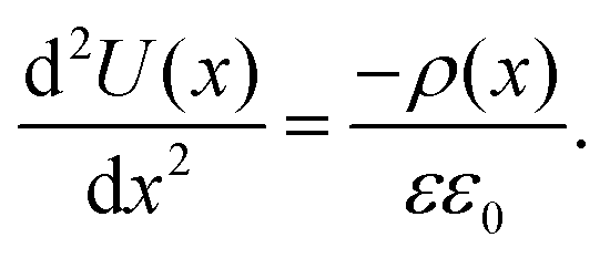 | (4) |
Conflicts of interest
There are no conflicts to declare.Acknowledgements
Partial financial support by the Deutsche Forschungsgemeinschaft (DFG) in the IRTG 1404 is acknowledged. Open Access funding provided by the Max Planck Society. We thank Dallas Murphy for his help in finding structure in the article and Amelie Axt, Alexander Klasen and David van Duinen for helpful discussions.References
- W. Tress, J. Phys. Chem. Lett., 2017, 8, 3106–3114 CrossRef PubMed.
- A. Pockett, G. E. Eperon, N. Sakai, H. J. Snaith, L. M. Peter and P. J. Cameron, Phys. Chem. Chem. Phys., 2017, 19, 5959–5970 RSC.
- V. W. Bergmann, Y. Guo, H. Tanaka, I. M. Hermes, D. Li, A. Klasen, S. A. Bretschneider, E. Nakamura, R. Berger and S. A. L. Weber, ACS Appl. Mater. Interfaces, 2016, 8, 19402–19409 CrossRef PubMed.
- M. Cai, N. Ishida, X. Li, X. Yang, T. Noda, Y. Wu, F. Xie, H. Naito, D. Fujita and L. Han, Joule, 2018, 2, 296–306 CrossRef.
- P. Calado, A. M. Telford, D. Bryant, X. Li, J. Nelson, B. C. O’Regan and P. R. F. Barnes, Nat. Commun., 2016, 7, 13831 CrossRef PubMed.
- R. A. Belisle, W. H. Nguyen, A. R. Bowring, P. Calado, X. Li, S. J. C. Irvine, M. D. McGehee, P. R. F. Barnes and B. C. O’Regan, Energy Environ. Sci., 2017, 10, 192–204 RSC.
- V. Roiati, E. Mosconi, A. Listorti, S. Colella, G. Gigli and F. De Angelis, Nano Lett., 2014, 14, 2168–2174 CrossRef PubMed.
- A. Guerrero, J. You, C. Aranda, Y. S. Kang, G. Garcia-Belmonte, H. Zhou, J. Bisquert and Y. Yang, ACS Nano, 2016, 10, 218–224 CrossRef PubMed.
- I. Zarazua, J. Bisquert and G. Garcia-Belmonte, J. Phys. Chem. Lett., 2016, 7, 525–528 CrossRef PubMed.
- J. Carrillo, A. Guerrero, S. Rahimnejad, O. Almora, I. Zarazua, E. Mas-Marza, J. Bisquert and G. Garcia-Belmonte, Adv. Energy Mater., 2016, 6, 1502246 CrossRef.
- O. Almora, A. Guerrero and G. Garcia-Belmonte, Appl. Phys. Lett., 2016, 108, 043903 CrossRef.
- G. Richardson, S. E. J. O’Kane, R. G. Niemann, T. A. Peltola, J. M. Foster, P. J. Cameron and A. B. Walker, Energy Environ. Sci., 2016, 9, 1476–1485 RSC.
- Y. Yuan, Q. Wang, Y. Shao, H. Lu, T. Li, A. Gruverman and J. Huang, Adv. Energy Mater., 2016, 6, 1501803 CrossRef.
- Y. Yuan, J. Chae, Y. Shao, Q. Wang, Z. Xiao, A. Centrone and J. Huang, Adv. Energy Mater., 2015, 5, 1500615 CrossRef.
- J. L. Minns, P. Zajdel, D. Chernyshov, W. van Beek and M. A. Green, Nat. Commun., 2017, 8, 15152 CrossRef PubMed.
- C. Li, A. Guerrero, Y. Zhong, A. Gräser, C. A. M. Luna, J. Köhler, J. Bisquert, R. Hildner and S. Huettner, Small, 2017, 13, 1701711 CrossRef PubMed.
- Y. Yuan and J. Huang, Acc. Chem. Res., 2016, 49, 286–293 CrossRef PubMed.
- J. S. Yun, J. Seidel, J. Kim, A. M. Soufiani, S. Huang, J. Lau, N. J. Jeon, S. I. Seok, M. A. Green and A. Ho-Baillie, Adv. Energy Mater., 2016, 6, 1600330 CrossRef.
- N. J. Jeon, J. H. Noh, Y. C. Kim, W. S. Yang, S. Ryu and S. I. Seok, Nat. Mater., 2014, 13, 897–903 CrossRef PubMed.
- Y. Bai, H. Yu, Z. Zhu, K. Jiang, T. Zhang, N. Zhao, S. Yang and H. Yan, J. Mater. Chem. A, 2015, 3, 9098–9102 RSC.
- C.-H. Chiang and C.-G. Wu, Nat. Photonics, 2016, 10, 196–200 CrossRef.
- Y. Hou, S. Scheiner, X. Tang, N. Gasparini, M. Richter, N. Li, P. Schweizer, S. Chen, H. Chen, C. O. R. Quiroz, X. Du, G. J. Matt, A. Osvet, E. Spiecker, R. H. Fink, A. Hirsch, M. Halik and C. J. Brabec, Adv. Mater. Interfaces, 2017, 4, 1700007 CrossRef.
- H.-S. Kim, I.-H. Jang, N. Ahn, M. Choi, A. Guerrero, J. Bisquert and N.-G. Park, J. Phys. Chem. Lett., 2015, 6, 4633–4639 CrossRef PubMed.
- Q. Jiang, L. Zhang, H. Wang, X. Yang, J. Meng, H. Liu, Z. Yin, J. Wu, X. Zhang and J. You, Nat. Energy, 2016, 2, 16177 CrossRef.
- J. Xu, A. Buin, A. H. Ip, W. Li, O. Voznyy, R. Comin, M. Yuan, S. Jeon, Z. Ning, J. J. McDowell, P. Kanjanaboos, J.-P. Sun, X. Lan, L. N. Quan, D. H. Kim, I. G. Hill, P. Maksymovych and E. H. Sargent, Nat. Commun., 2015, 6, 7081 CrossRef PubMed.
- V. W. Bergmann, S. A. L. Weber, F. Javier Ramos, M. K. Nazeeruddin, M. Grätzel, D. Li, A. L. Domanski, I. Lieberwirth, S. Ahmad and R. Berger, Nat. Commun., 2014, 5, 6001 Search PubMed.
- R. Berger, A. L. Domanski and S. A. L. Weber, Eur. Polym. J., 2013, 49, 1907–1915 CrossRef.
- C.-S. Jiang, M. Yang, Y. Zhou, B. To, S. U. Nanayakkara, J. M. Luther, W. Zhou, J. J. Berry, J. van de Lagemaat, N. P. Padture, K. Zhu and M. M. Al-Jassim, Nat. Commun., 2015, 6, 8397 CrossRef PubMed.
- L. Collins, M. Ahmadi, T. Wu, B. Hu, S. V. Kalinin and S. Jesse, ACS Nano, 2017, 11, 8717–8729 CrossRef PubMed.
- E. M. Tennyson, C. Gong and M. S. Leite, ACS Energy Lett., 2017, 2, 2761–2777 CrossRef.
- S. T. Birkhold, J. T. Precht, R. Giridharagopal, G. E. Eperon, L. Schmidt-Mende and D. S. Ginger, J. Phys. Chem. C, 2018 DOI:10.1021/acs.jpcc.8b03255.
- C. Eames, J. M. Frost, P. R. F. Barnes, B. C. O’Regan, A. Walsh and M. S. Islam, Nat. Commun., 2015, 6, 7497 CrossRef PubMed.
- Y. Shao, Y. Fang, T. Li, Q. Wang, Q. Dong, Y. Deng, Y. Yuan, H. Wei, M. Wang, A. Gruverman, J. Shield and J. Huang, Energy Environ. Sci., 2016, 9, 1752–1759 RSC.
- I. Anusca, S. Balčiūnas, P. Gemeiner, Š. Svirskas, M. Sanlialp, G. Lackner, C. Fettkenhauer, J. Belovickis, V. Samulionis, M. Ivanov, B. Dkhil, J. Banys, V. V. Shvartsman and D. C. Lupascu, Adv. Energy Mater., 2017, 1700600 CrossRef.
- E. Ghahremanirad, A. Bou, S. Olyaee and J. Bisquert, J. Phys. Chem. Lett., 2017, 8, 1402–1406 CrossRef PubMed.
- H. J. Butt, K. Graf and M. Kappl, Physics and Chemistry of Interfaces, Wiley-VCH, Weinheim, 2003 Search PubMed.
- A. Walsh, D. O. Scanlon, S. Chen, X. G. Gong and S.-H. Wei, Angew. Chem., 2015, 127, 1811–1814 CrossRef.
- J. Will, Y. Hou, S. Scheiner, U. Pinkert, I. M. Hermes, S. A. L. Weber, A. Hirsch, M. Halik, C. Brabec and T. Unruh, ACS Appl. Mater. Interfaces, 2018, 10, 5511–5518 CrossRef PubMed.
- P. Lopez-Varo, J. A. Jiménez-Tejada, M. García-Rosell, J. A. Anta, S. Ravishankar, A. Bou and J. Bisquert, ACS Energy Lett., 2017, 2, 1450–1453 CrossRef.
- W. Tress, J. P. Correa Baena, M. Saliba, A. Abate and M. Graetzel, Adv. Energy Mater., 2016, 6, 1600396 CrossRef.
- L. Collins, S. Jesse, J. I. Kilpatrick, A. Tselev, O. Varenyk, M. B. Okatan, S. A. L. Weber, A. Kumar, N. Balke, S. V. Kalinin and B. J. Rodriguez, Nat. Commun., 2014, 4871 Search PubMed.
- L. Contreras, J. Idígoras, A. Todinova, M. Salado, S. Kazim, S. Ahmad and J. A. Anta, Phys. Chem. Chem. Phys., 2016, 18, 31033–31042 RSC.
- H. J. Snaith, A. Abate, J. M. Ball, G. E. Eperon, T. Leijtens, N. K. Noel, S. D. Stranks, J. T.-W. Wang, K. Wojciechowski and W. Zhang, J. Phys. Chem. Lett., 2014, 5, 1511–1515 CrossRef PubMed.
- J. Xing, Q. Wang, Q. Dong, Y. Yuan, Y. Fang and J. Huang, Phys. Chem. Chem. Phys., 2016, 18, 30484–30490 RSC.
- J. L. Garrett and J. N. Munday, Nanotechnology, 2016, 27, 245705 CrossRef PubMed.
- D. Ziegler and A. Stemmer, Nanotechnology, 2011, 22, 075501 CrossRef PubMed.
- R. Giridharagopal, G. E. Rayermann, G. Shao, D. T. Moore, O. G. Reid, A. F. Tillack, D. J. Masiello and D. S. Ginger, Nano Lett., 2012, 12, 893–898 CrossRef PubMed.
Footnote |
| † Electronic supplementary information (ESI) available. See DOI: 10.1039/c8ee01447g |
| This journal is © The Royal Society of Chemistry 2018 |