
 Open Access Article
 This Open Access Article is licensed under a Creative Commons Attribution-Non Commercial 3.0 Unported Licence
Understanding the non-covalent interaction mediated modulations on the electronic structure of quasi-zero-dimensional graphene nanoflakes†
Amrit
Sarmah
 *ab and
Pavel
Hobza
ab
*ab and
Pavel
Hobza
ab
aInstitute of Organic Chemistry and Biochemistry of the Czech Academy of Sciences, Flemingovo nam. 2, CZ-16610 Prague 6, Czech Republic. E-mail: amrit.sarmah@uochb.cas.cz
bDepartment of Physical Chemistry, Palacký University, CZ-77146 Olomouc, Czech Republic
First published on 11th June 2018
Abstract
In recent years, magnetic or electric field induced modulations on the electronic environment of single molecular systems are common practice. In this particular study, we have instigated the possibility of controlling the electronic and spin-dependent properties of hydrogen-terminated graphene fragments, so-called graphene nanoflakes (GNF), using weak non-covalent interactions as the external stimuli. The topological frustration in the graphene fragment appreciated the compelling electronic behavior of the system. This leads to some unorthodox spin-distribution in the system and it is possible to synchronize this electronic perturbation switching through a non-covalent interaction. These findings institute a new avenue for sculpting such donor–acceptor composites as self-regulated spintronic devices in next generation electronics.
1. Introduction
Low dimensional atomically precise carbon-based magnetism1 consisting of a 2D graphene backbone is anticipated to be the most suitable building-block for the fabrication of next-generation electronic and spintronics devices.2 The higher Curie temperature and relatively large spin correlation length compared to those of conventional magnets are primarily responsible for the exquisite features in the carbon-based magnetic nanostructures.3 In a recent technological breakthrough, the laboratory synthesized true two-dimensional (2D) graphene crystals, which generated massive excitement among the scientific community across the globe.4,5 Subsequent sophisticated investigations of this system revealed different, extraordinary electronic properties such as the room-temperature quantum hall effect,6 half-metallicity,7 massless quasi-particles,8 high mobility and coherence,4etc. Although developing a precise understanding of these properties accounts for some fundamental perspectives, these have considerable implications on high-end technological developments as well. On the lower side, the inherent zero bandgap and semi-metal characteristics are the severe impediments that restrain the feasibility of carbon-based electronics. Certain promising topological modifications to the 2D graphene crystal lattice to engineer a small band gap are nanostructuring graphene into carbon nanotubes (CNTs) and graphene nanoribbons (GNRs) or nanoflakes (GNFs).9,10 Many high-quality experimental research efforts have been devoted to understanding the optoelectronic properties of these different topological analogs from graphene, namely GNRs11–14 and armchair GNFs of triangular,15 hexagonal16,17 and other shapes.18,19 The scientific community is highly optimistic about the GNR based device fabrication for DNA sequencing along with sophisticated spintronic applications.20–22GNRs are composed of finite-size one-dimensional (1D) straight edges, whereas GNFs are quasi-zero-dimensional graphene quantum dots and are, in principle, part of a large hexagonal carbon network in reduced dimensions. It is important to understand that the building-blocks or the functional components of nanoscale devices should, at the nanometer scale, provide sustainable performance according to Moore's law. It is encouraging to note that, the recent experiments ensure the possibilities of obtaining the graphene features at the scale of tens of nanometers.2 Perhaps the quantum confinement attributed to the reduced dimensionality along with the modification of the topological edge-states actuate unique electronic and magnetic properties in the GNFs. The elegant electronic characteristics and contemplation of the application prospects of GNFs have been extensively explored in some recent experimental studies.23–26 It is worth mentioning here that the impact of relative variations in size and edge-states on the overall electronic structure of relatively large (lateral dimension up to 20 nm) GNFs has been experimentally demonstrated.27 Localized edge states along with the metallic features are observed in ZZGNFs. The point or extended defect and chemical modification induced magnetism on the non-magnetic graphene crystal is well documented in literature.28–31 On the other hand, the non-trivial π-electron-driven magnetism is the consequence of localized edge-states in a zero-dimensional (0D) graphene nanoflake (GNF).32,33 Successful nanofabrication of graphene materials is attributed to contemporary ground-breaking scientific developments,34,35 but the controlled growth of a specific edge-type is still challenging. Sophisticated nanofabrication techniques combined with scanning tunneling microscopy produced precise zigzag edges, namely nanoribbons with substantially high long-range magnetic ordering at room temperature.36 Interestingly, a transition from semiconductor to metallic state followed by substantial changes to the magnetization of the edge-states, comparable to that of the ribbon width, has also been realized.36 The systematic analysis of the conformational changes in the halogen–pi interaction, as depicted by Kim et al., opens-up a new perspective towards size-dependent electronic tuning in the hexagonal carbon network.37
It is worth mentioning here that the implicit non-covalent functionalization through the physisorption of electron withdrawing/donating molecules is the implication of a relatively non-destructive and straightforward way to obtain dope graphene.38,39 To be precise, the induced doping effect on the graphene surface is the consequence of a charge transfer interaction between the composite pair. Most importantly, the graphene surface institutes minimal deformation due to the predominate van der Waals (vdW) interaction and also maximizes the possibility of the cooperative doping effect. Different experimental and theoretical investigations have been performed to realize the efficient doping of the 2D graphene surface in terms of non-covalent interactions. From the experimental prospects, Voggu et al. successfully carried out p- and n-doping on the graphene surface using specific donor molecules, tetrathiafulvalene (TTF) and some acceptor counterparts like tetracyanoethylene (TCNE).39 In another significant contribution, Chen and co-workers designed some doping protocols using the strong acceptor molecule, tetrafluoro-tetracyanoquinodimethane (F4-TCNQ), to induce p-doping on the surface.38 The high-end DFT calculation contributes new insights to this exciting topic. Different groups reported extensive computational simulation results on the non-covalent functionalization of graphene, based on typical electron donors and acceptors such as TTF,40 TCNE,41 and F4-TCNQ.42 Cho et al. performed extensive theoretical investigations to develop a better understanding on the adsorption dynamics of nucleobases on the graphitic surface.43 However, none of these reported works realized an opportunity to implement the principle of non-covalent functionalization to account for the size and shape dependent electronic modulations on the zero-dimensional (0D) graphene nanoflakes (GNFs). The non-destructive and reversible nature of functionalization is anticipated to be a pivotal signature to implement the concept in some practical nanoelectronic applications.
In recent years a great deal of research effort has been devoted towards the non-covalent functionalization of graphene. However, to the best of the authors’ knowledge, the present study is a systematically organized and compact approach to address a few unexplored aspects of non-covalent interaction arbitrated electronic modulations in graphene nanoflakes. Here, first-principles DFT calculations are used to highlight the acclaimed changes in electronic and magnetic properties of the GNF–HATCN nanocomposites. It is important to note that the electronic environment in quantum dots is mainly sensitive to the shape and size of the system. Therefore, we embodied GNFs constituting different sizes as well as shapes. Subsequently, a strong pi–acceptor molecule, hexaazatriphenylene-hexacarbonitrile (HATCN) (see Fig. S1 in the ESI†), considerably enhanced the effect of the non-covalent interaction on the GNFs. The six CN groups in the molecule substantially enriched the electron accepting ability of the system. From here onwards we shall use ‘HATCN’ as the short-hand notation for this molecule.
The paper is organized in the following way: Section 2 contains a brief discussion regarding the implemented computational methodologies along with some relevant information about the model systems. A broad interpretation of the computed data is included in Section 3 and it is sub-divided into two sections. Some of the essential electronic characteristics of the five modeled GNF systems are discussed in Section 3(a). The different electronic and magnetic properties of the donor–acceptor (GNF–HAT) composite systems and their probable futuristic device application prospects are analyzed in Section 3(b). Finally, Section 4 consists of specific concluding remarks on these particular nanocomposites and the possibilities of using non-covalent interactions to regulate the electronic and magnetic properties of nanostructures.
2. Computational details
DFT calculations were performed using the open source Quantum Espresso 5.4.0 code.44 We used Troullier and Martins45 norm-conserving pseudopotentials and exchange–correlation (xc) effects are incorporated at the Becke–Lee–Yang–Parr (BLYP)46 level of the generalized gradient approximation (GGA). The van der Waals correction to the calculations has been incorporated through semi-empirical Grimme's DFT-D2 methodology47 as implemented in Quantum Espresso. The standard kinetic energy cutoff for wavefunctions is set at 40 Ry and the corresponding cutoff for charge density and potential is set at 160 Ry. As we have discussed previously, the electronic environment of GNFs has a strong dependence on the size and shape of the system. In the present study, we considered five different types of model GNF structures containing zigzag edges. The reciprocal space integrations were performed at the ‘Γ’ point. Within the extended periodic framework of the calculations, the flakes were considered to be placed in simple cubic supercells such that the periodic images were separated by at least 10 Å and 5–8 Å vacuum space in the vertical and horizontal directions, respectively, to maintain some negligible interactions between the repetitive units. Subsequently, we have performed several convergence tests w.r.t. the different supercell lengths to determine the ground state of the system. Indeed, a 10 Å vacuum space along the Z-direction seems to be the most preferred situation to obtain the energy minima for the system. Nanoflakes were optimized until the forces on each atom were less than 5 × 10⁻³ eV Å−1. The forces on the modeled nanoflakes were minimized up to <10−3 Ry a.u.−1 for all atoms to obtain fully relaxed atomic geometries. In the model systems, the dangling bonds at the edge atoms are saturated with atomic hydrogens. To understand the impact of shape and size of the GNFs on their electronic environment, we included five different zigzag edge GNF structures (Fig. 1). Furthermore, the topological defects on the GNF are significant to interpret the electronic modulations in the system. To account for this particular feature, we have included two special cases (last two GNF structures in Fig. 1) with existing structural defects. In the composite system, the HATCN molecule is bound to the GNF predominantly through a weak van der Waals type interaction. The acceptor HATCN seems to be strongly physisorbed on the GNF surface. For computational convenience, we have assumed that the GNF is a part of the extended graphene network saturated with atomic hydrogens. We can argue that the π–π stacking interaction is more favorable for the HATCN–GNF nanocomposite (due to the flat surface structure of both the systems) rather a covalent complex formation. However, we cannot rule out the possibility of covalent complex formation too. In such a situation, the acceptor HATCN will drift to one of the edges of the GNF as electronic charges mostly tend to accumulate on the edges.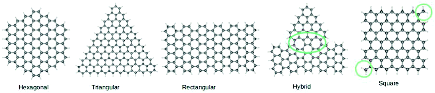 | ||
| Fig. 1 Relaxed hydrogenated graphene nanoflake (GNF) structures modeled for our present study. We have included different shapes and sizes to account for the topological changes induced electronic modulations in the system. The ‘Hybrid’ and ‘Square’ systems contain certain defects in the lattice as depicted by green circles. | ||
3. Results and discussions
(a) Impact of topological changes to the electronic and magnetic environment of single layered graphene nanoflakes (GNFs)
In this section, we will attempt to probe the observed modulations to the electronic environment of GNFs as a result of their topological changes. We have considered five GNF structures with different shapes and sizes along with some defects. The relaxed structures of the model GNFs are given in Fig. 1. It is well established that the intrinsic electronic properties of the GNFs are related to the size and shape of the system. The impact of structural orientation on the electronic charge distribution of five GNFs (from contour plots in the [110] plane) is portrayed in the ESI† (Fig. S2). Some characteristic changes to the symmetric distortion of the electronic charges on the hexagonal and hybrid GNF surfaces are perhaps prevalent in the figure.It is also essential to shed some light on the edge effect of GNR/GNFs before extending the strategic discussion on the noncovalent interaction mediated electronic modulations. The characteristic charge accumulations on the edges are realized for the GNR based nanostructures. The external transverse electric field induced perturbations to the electronic and magnetic properties of pristine and edge-decorated zGNRs are well documented.48 Systematic and controlled chemical modifications to the edges of zGNR lead to an effective decrease in the observed half-metallicity or nonmagnetic behaviors in zGNRs. Some recent scientific developments accounted for the temperature dependence of graphene edge termination at the atomic scale.49 This particular experimental study showcased the effect of temperature variations in the edge-state electronic environment of GNRs. At some relatively low temperatures (below 4000 °C) the zigzag terminations are prevalent for the graphene edges. On the other hand, the edges are dominated by armchair and reconstructed zigzag edges above 6000 °C.
It is worth mentioning here that the shape and size of the nanoflakes have substantial impact on the intrinsic magnetic properties of the system. The magnetic behavior of the five different systems is reported in Fig. 2. Here, the ground state magnetization densities in terms of up (down) spin densities are represented as red (blue) isosurface plots. Subsequently, the graphical representations of the total and absolute magnetic moment values for the five systems are also included in Fig. 2. As can be seen in the hexagonal nanoflake, spherical symmetry of the system is preserved and predicted the absence of any magnetic moment for the structure. So, in principle, the hexagonal nanoflake should be non-magnetic in nature. The triangular nanoflake exhibits typical edge-state magnetism. Relatively higher total and absolute magnetic moment values are observed for this structure. The anti-ferromagnetic ordering of the spin arrangement is dominant along the edges.
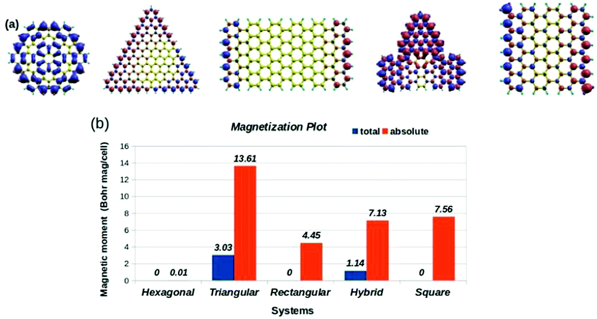 | ||
| Fig. 2 The magnetic structures of the nanoflake (a) spin density distribution isosurface plots for the five GNFs and (b) corresponding computed total (the integral of the magnetization in the cell) and absolute (the integral of the absolute value of the magnetization in the cell) magnetic moment values. The red and purple color regions in the isosurface plots represent the oppositely aligned excess spin densities. | ||
However, the spin alignment in the triangular GNF is not uniform throughout the edges. It is evident from Fig. 2 that on the contrary to an excess of up-spin densities along the edges, the right-hand corner of the edge experienced sudden growth of excess spin densities with down-spin states. The spin densities are localized at the two opposite edges of the rectangular nanoflake. The possibility of anti-ferromagnetic spin coupling between the two opposite edges is distinct in the system. Subsequently, coupling results in zero total magnetic moment in the system, but there are some specific values for the absolute magnetic moment of the system. The hybrid nanoflake attributes specific magnetic moment in the system. The structure is the combination of triangular and rectangular motifs. The magnetic moment in the system is the consequence of the localized spin densities towards the edges of the rectangular fragment. The square fragment also has a significantly low total magnetic moment due to the anti-ferromagnetic interaction between the spin densities located at the two edges. The typical edge-state magnetization is prevalent in all the nanoflake systems.
2D electronic charge density distribution maps for the systems are included in the ESI† (Fig. S2). A uniform electronic charge distribution along the surface of the three nanoflake systems is evident from the figure. However, some anomalous signature has been accounted for in the hexagonal and hybrid systems. Here, the electronic charge localization is observed in some particular regions. The location of the frontier molecular orbitals (FMOs) is an interesting aspect of the GNFs. The computed HOMO–LUMOs are depicted in Fig. 3. Depending on the shape of the GNFs some significant variation in the symmetry of the FMOs has been accounted for, as shown in the figure. In the hexagonal system, the HOMO and LUMO are symmetric in nature. The lobes are symmetrically spread along the surface. The HOMO in the triangular GNF is localized more towards the edges while the LUMO is squeezed to the center of the system. In the rectangular system, the FMOs are concentrated at the two opposite edges. The hybrid system has some different symmetric orientations for the FMOs, as the HOMO is mainly located on the rectangular part whereas the triangular portion of the structure hosts the LUMO. Similarly, for the square GNF, the HOMO contributions have appeared along the edges, and the LUMO is distributed across the whole structure.
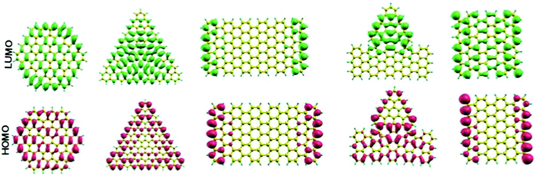 | ||
| Fig. 3 The highest occupied level (HOMO) and corresponding lowest unoccupied level (LUMO) colored in red (bottom panel) and green (top panel), respectively, for the GNF systems. | ||
(b) Non-covalent interaction induced modulations to the electronic environment
In this section we shall systematically evaluate the possibilities of non-bonding interactions as effective external stimuli to tune the electronic properties of graphene nanoflakes (GNFs). As we know, the GNF surface has some inherent electron donor characteristics, so a strong electron acceptor is imperative to induce electronic modulation to the system. The overall system will behave as a composite donor–acceptor nanostructure. Subsequently, the explicit charge transfer between the two components effectively regulates the electronic environment of the GNF. Indeed, the non-covalent functionalization with organic molecules accounts for reversible electronic perturbations on the graphene. Perhaps the weak van der Waals type interactions between the π-orbitals of the planar organic molecule and graphene are the origin of observed electronic changes in the system. Recently, this simple functionalization technique has been exploited to modify the electronic properties of a graphene surface with different organic molecules such as tetrafluorotetracyanoquinodimethane (F4-TCNQ),50 3,4,9,10-perylenetetracarboxylic dianhydride (PTCDA),51etc. In search of a suitable surface modifier, hexaazatriphenylene hexacarbonitrile (HATCN) turns out to be an ideal candidate. Some recent computational studies on HATCN/graphene accounted for the significant work function (Φ) modification along with the persistence of large charge carrier mobilities in the resulting doped graphene surface.52 Also, this molecule has a considerable electron affinity (EA) that pushes the lowest unoccupied molecular orbital (LUMO) level close to the Fermi level of an electrode.53 The electronic properties of HATCN are well documented in the literature.54,55The zero-dimensional GNFs appeared to have a flat surface similar to that of graphene with the characteristic edge-states. To assess the electronic fingerprint of non-covalent functionalization on the GNFs, the HATCN molecule is placed horizontally on top of the GNFs in our model systems. We have systematically screened a number of different initial structural conformations of HATCN adsorbed on the GNF surface. It is worth mentioning here that the observed relative energy difference is found to be negligible for the different conformations. Out of the tested orientations, our current study will be concentrated on the most stable configurations. The relaxed geometries of the systems are reported in Fig. 4. In the subsequent sections, we will elaborate the comprehensive understandings on the relative changes to the electronic environment of different GNFs by the non-covalent functionalization with HATCN.
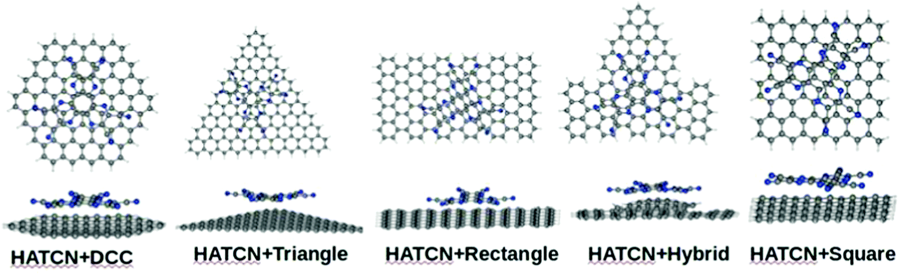 | ||
| Fig. 4 The relaxed structures of the GNF–HATCN composite system. The top is the vertical view of the system, and below is the horizontal view. | ||
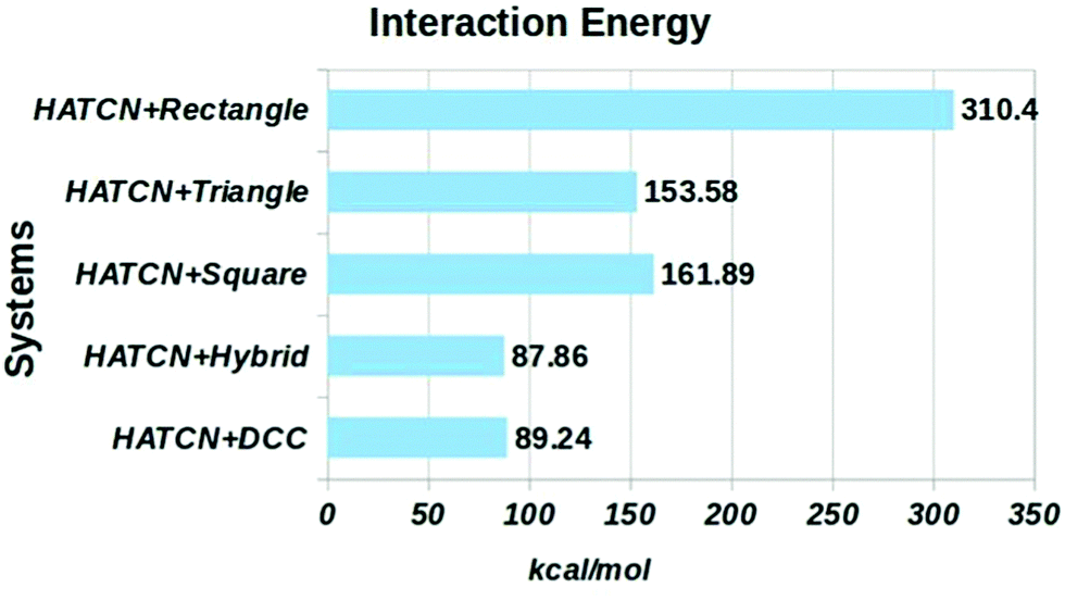 | ||
| Fig. 5 The interaction energy plots for the five GNF–HATCN composite systems. The energy value is calculated as Interaction Energy = EGNF–HATCN − (EGNF + EHATCN). | ||
As observed from the interaction energy plots, the size and shape of the GNFs proclaimed distinct variations in the overall stability of the nanostructures. The nanoflake systems with hexagonal (DCC) and hybrid structures are predicted to have relatively lower stability with HATCN. Again, the non-covalent interaction between HATCN and the rectangular GNF nanocomposite institutes the highest stability among the considered systems. Similarly, the structures with square and triangular shaped GNFs and HATCN showed substantial improvements in their thermodynamic stabilities compared to those of the hexagonal and hybrid systems. It can be realized that depending on the size and shape of the GNFs there are some significant changes to the overall stability of the combined systems. Predominantly, dispersion interactions between the HATCN and GNF holds the two fragments and an associated charge transfer provides the additional increment to the overall stability.
The resulting changes in the electronic states predominantly arise from the variation in size and shape of the GNFs. The symmetric distribution of the electronic energy states for the up and down spin electrons is prevalent in the hexagonal-HATCN system. A fully compensated ferrimagnetic ordering in the system is also accounted for in these symmetric DOS patterns. The intense peaks at the Fermi level indicate the possibility of intermolecular charge transfer in the system. Interestingly, some half-metallic conducting nature of the electrons is evident for the triangular-HATCN system. Here, electrons in the up-spin channel show metallic properties while the down-spin electrons seem to have an insulating nature. The rectangular flake remained half-metallic but alters electronic energy states at the Fermi level. As can be seen from the figure that the down-spin electron channels located below the Fermi level are associated with metallic behavior. The nanocomposite consisting of the hybrid GNF exhibits metallic characteristics. The ferromagnetic spin arrangement in the system can also be realized from the DOS spectrum. The electronic structure in the square-HATCN system is qualitatively similar to that of the triangular GNF composite. The up-spin channels are populated at the Fermi level and there is a substantial energy gap between the highest occupied and lowest unoccupied states in the down-spin channels. This represents the ideal half-metallic nature of the system. The majority of the systems considered in the present study remain half-metallic upon interaction with HATCN. Perhaps these hypothetical systems anticipated manifesting comprehensive spin-polarized transport under certain gate voltage. Furthermore, the findings pertained certain control over the electronic conduction in a particular channel by tuning the polarity of the gate voltage in the composite structures. It is apparent that the structural features of the GNFs along with external stimuli, such as HATCN, are effective tools to regulate spin-polarized transport in such systems.
The relative contributions of different atoms present in the system toward the overall electronic structure provide a comprehensive understanding of the electronic transport properties of the nanocomposite. Subsequently, Fig. 6 depicts the spin-polarized partial density of states (PDOS) plot for the different systems. Here, red and black lines represent the density of spin up and down p-electrons of carbon atoms, whereas the filled regions (inside the plots) are the contributions from the p-electrons of the nitrogen atoms (spin up and down) present in HATCN. The substantial contributions from the nitrogen p-electrons at the Fermi level are evident from the figure. It can also be argued that the inherent half-metallic nature of the systems is mainly influenced by the presence of the nitrogen atoms. It is observed that the electronic states of the nitrogen atoms are the solo contributors to the down-spin channels at the Fermi level to impart half-metallicity to the system. This institutes some persuasive indication that the non-covalent interaction induced tuning of electronic properties in GNF probably has some vital importance in the context of spin-based electronics.
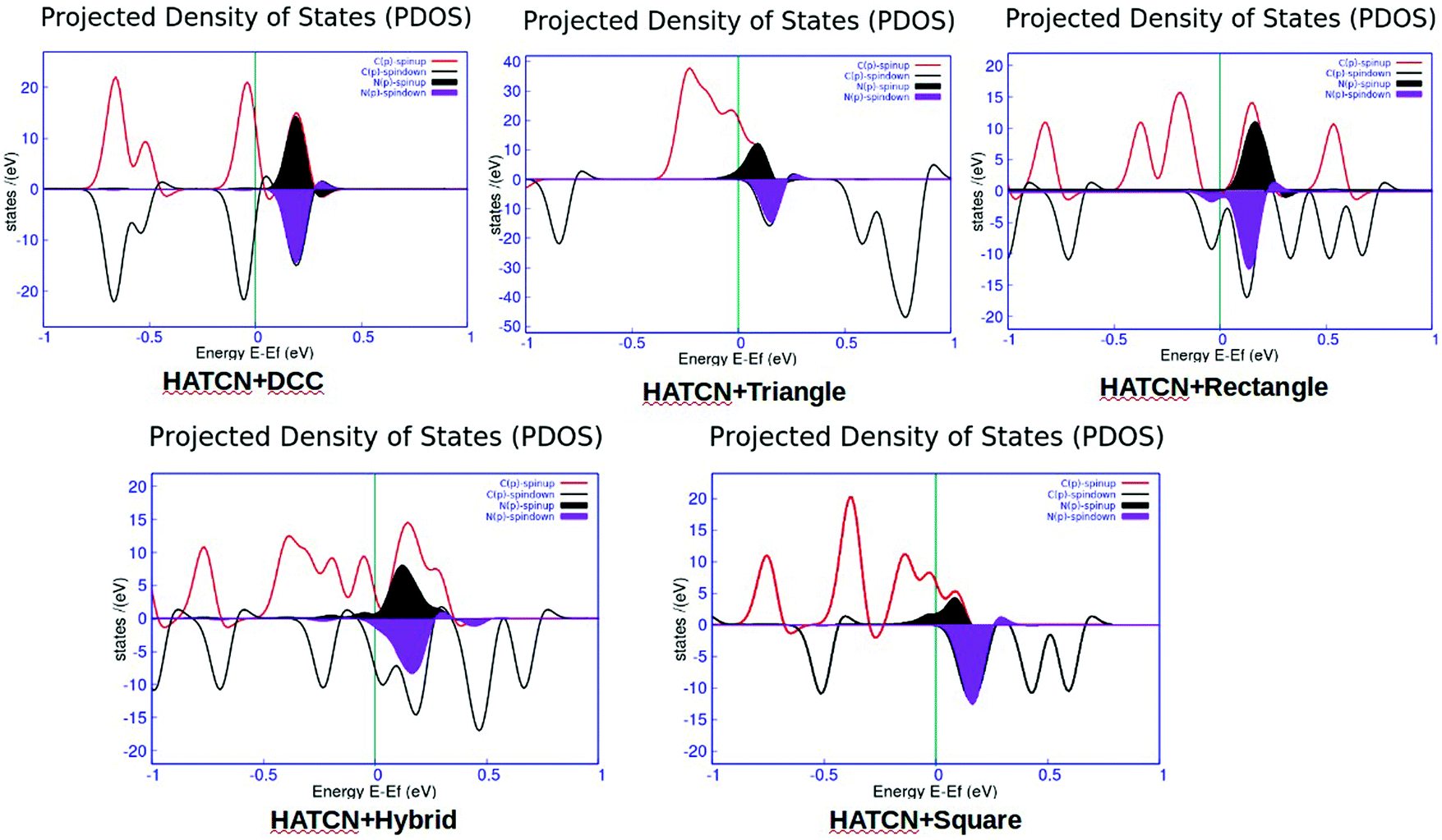 | ||
| Fig. 6 The projected density of states (PDOS) plots for the five different GNF–HATCN nanosystems. Here, the Fermi level is set at zero. | ||
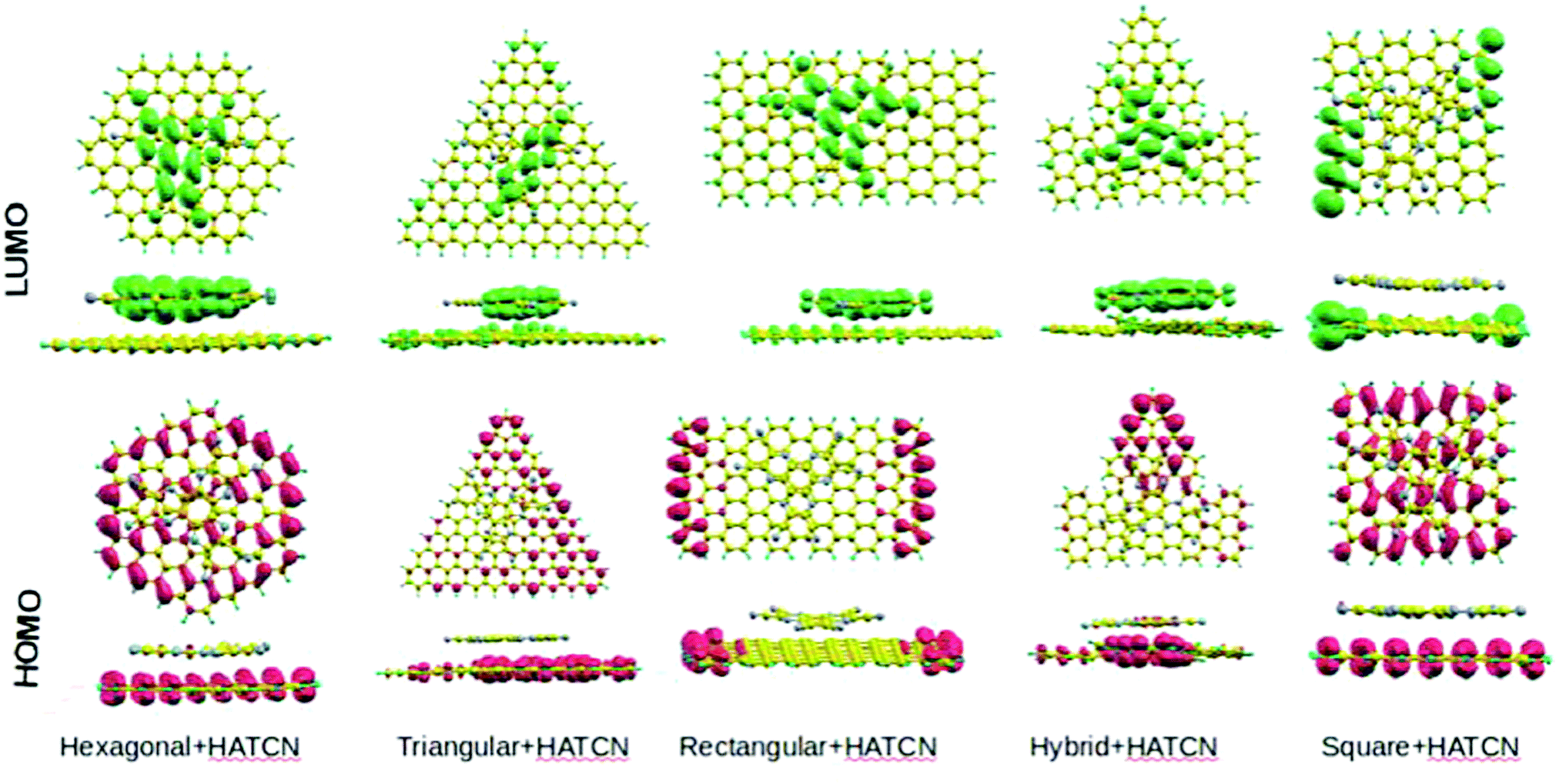
The propagations of an electronic wavefunction at the valence band maxima (VBM) and conduction band minima (CBM) are reported in Fig. 7. The VBM is concentrated on the GNFs, and the CBM is primarily located on the acceptor part of the composite system. This indicates higher probabilities for the through-space charge transfer between the two fragments. In the hexagonal system, the VBM is symmetrically distributed throughout the GNF sheet, and the CBM is positioned at the HATCN. On the other hand, the VBM is mostly concentrated on one of the edges of the GNF in the triangular system, and some asymmetric isosurface densities for the CBM are accounted for in the figure. The rectangular system exhibited well-separated edge-state VBMs, positioned at the GNF followed by the presence of symmetric CBM state identities at the HATCN. In the hybrid GNF–HATCN composite, the VBM is positioned at the triangular part of the system, while the CBM is primarily concentrated at the HATCN. We have observed some distinct changes in the distribution of FMOs for the square-shaped GNF system. Here, both the VBM and CBM wavefunctions are located on the GNF sheet with different symmetries. It is worth mentioning here that we have observed some substantial changes in the HOMO–LUMO gap values for the systems. The graphical representation of the HOMO–LUMO gap values is reported in Fig. 8. It is quite convincing that the shape of the GNF system has significant impact on the overall HOMO–LUMO gap of the system. As we have seen (Fig. 8), the hybrid-HATCN and triangle-HATCN composite systems have the lowest and highest gap values, respectively.
 | ||
| Fig. 7 The highest occupied level (Valance Band Maxima, VBM) and corresponding lowest unoccupied level (Conduction Band Minima, CBM) colored in red (bottom panel) and green (top panel), respectively, for the systems. | ||
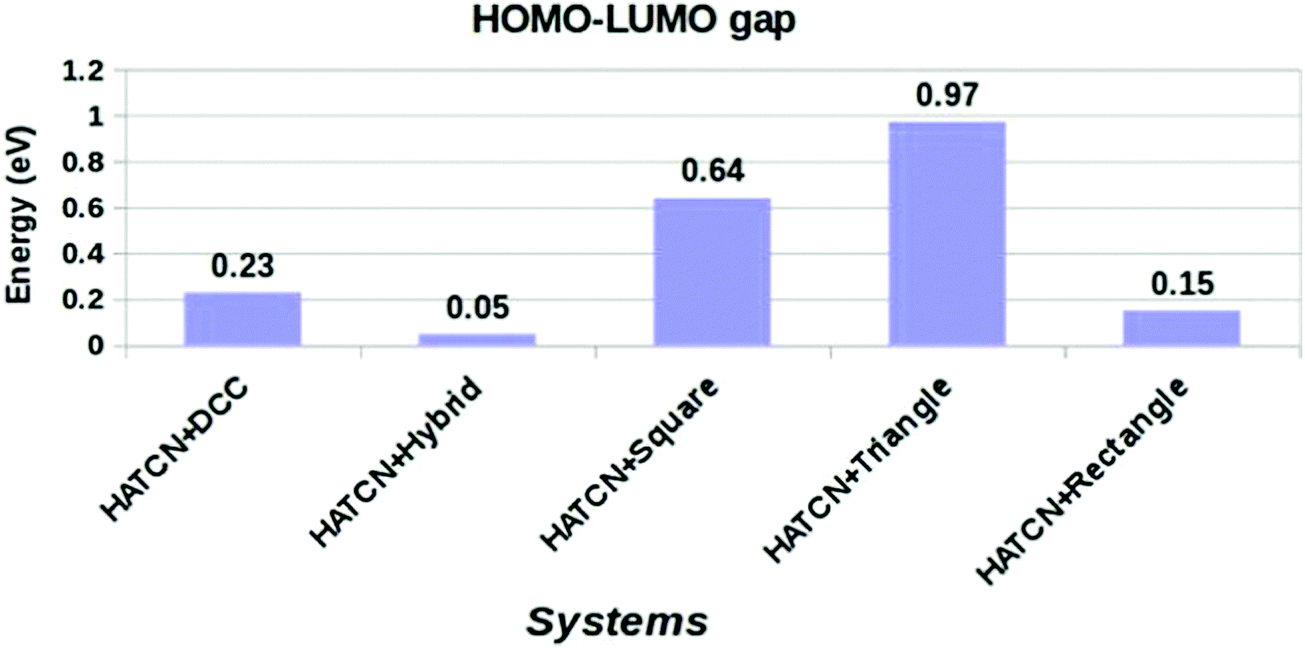 | ||
| Fig. 8 Graphical representations of the computed HOMO–LUMO gap values for the five systems in ascending order. | ||
The important aspect of the present study is the fabrication of non-covalent interaction mediated stable donor–acceptor nanocomposites and understanding the possible tuning of the electronic properties of the systems. The electronic structure, as well as the chemical nature, of a system is primarily dependent on the properties of frontier molecular orbitals. As we have discussed, the qualitative interpretations of the computed FMO pictures along with the relative HOMO–LUMO gap values provide certain strategic realizations to our concept. Perhaps there are two parameters that control the electronic changes in the system. To accomplish this task, we kept the acceptor (HATCN) fixed and varied the donor (GNFs) to regulate the desirable changes to the electronic properties of the combined system. It is worth mentioning here that the non-covalent interaction of the GNFs with a strong acceptor develops some conceptual understandings on the promising aspect of non-destructive and reversible functionalization of carbon quantum dots.
We have discussed the magnetic properties of single layer GNFs in the previous sections. Subsequently, some distinct changes to the original spin-arrangement have been observed for the GNFs upon the incorporation of HATCN. The computed 3D isosurface spin density maps are depicted in Fig. 9. Inevitably, the non-covalent interactions trigger observable modulations to the spin-dependent electronic properties of the GNFs. A pictorial representation of the total magnetic moment values for the composite systems is included in the ESI† (Fig. S4). The symmetric spin arrangement in the hexagonal system does not have a noticeable impact due to the introduction of HATCN, and the spin distribution almost remains the same as that of the isolated GNF. However, HATCN imparted substantial changes to the spin-arrangement in the triangular GNF system. We have observed the effect of spin reorganization in the spin density distribution upon placing HATCN above the triangular GNF surface. The growth of opposite spin densities at one of the edges of the isolated triangular GNF system has been suppressed, and the typical edge-state anti-ferromagnetic spin arrangement is consistent along the edges of the nanostructure. Similar observations are also accounted for in the rectangular GNF. Anti-ferromagnetically coupled edge-state magnetism is prevalent in the isolated rectangular GNF system, but the incorporation of HATCN on top of the GNF activates the development of strong ferromagnetically coupled states between the opposite edges. The non-covalent interaction between the systems regulates the observed spin transition. The hybrid GNF also shows changes to the spin orientation in the presence of HATCN. The excess spin density growth on the HATCN surface is prevalent in the composite structure. The typical anti-ferromagnetic spin arrangement is prominent at the triangular portion of the system followed by a substantial decrease in spin densities on the rectangular region. The spin rearrangement effect is also observed in the square GNF and HATCN system. As we have seen the particular anti-ferromagnetic spin orientations in the two opposite edges is predominant in the isolated GNF. Subsequently, the non-covalent as well as charge transfer interactions between the two fragments lead to the formation of ferromagnetically coupled edge-state spin orientations. The graphical pattern of the total magnetization is similar to that of the HOMO–LUMO gaps reported in the study. As we have emphasized, the non-covalent interaction mediated modulations to the spin states is also a reversible process. Subsequent removal of the external stimuli restored the original magnetic behavior of the GNF system. The induced changes are not permanent, and the effective modulations can be turned on/off by inclusion of the donor fragment. Indeed, the shape and size of the GNF is a vital tuning parameter to synchronize the changes.
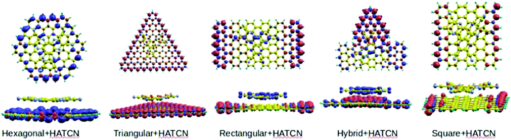 | ||
| Fig. 9 The isosurface spin density distribution plots for the five different GNF–HATCN nanocomposites. The red and purple colored regions in the plot represent the oppositely aligned excess spin densities. | ||
| Δρ(z) = ρ(z)combined − (ρ(z)GNF + ρ(z)HATCN) | (1) |
 | (2) |
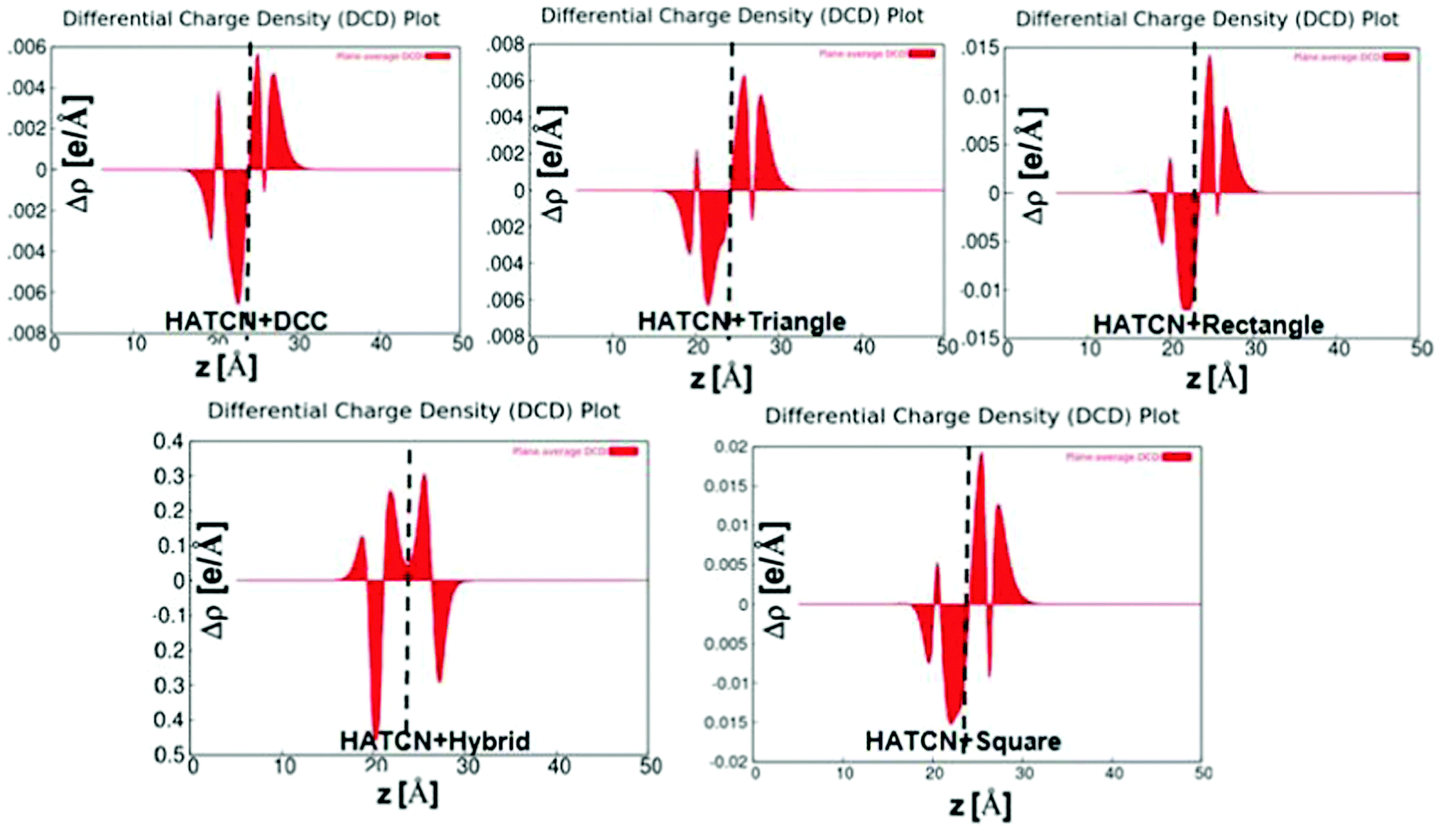 | ||
| Fig. 10 The planar average differential charge density (DCD), Δρ(z), plots for the HATCN–GNF nanocomposite systems, w.r.t the distance along the z-axis z[A′]. The black dotted line highlights the interfacial position. Here, the positive and negative values provide some quantitative approximations to the electron depletion and accumulation, respectively. | ||
4. Conclusions
We have investigated the emergence of non-covalent interaction mediated modulations on the electronic properties of graphene nanoflakes. The experimental realization for controlled preparation of GNFs with a wide range of size variation (ranging from several nanometers to a few hundred nanometers) already exists.56 Our DFT calculations suggest that controlled perturbations can be introduced to the electronic structure of GNFs through non-covalent interactions with strong π-acceptor systems. Essentially, the observed electronic changes are temporary and are effectively turned-off by removing the external stimuli. Our present study also shed some light on the unconventional functionalization of zero-dimensional GNF using a non-destructive pathway. The electronic behavior of these donor–acceptor composites is analyzed by different computed parameters. Eventually the shape and size dependent critical changes to the electronic properties of the systems are also systematically evaluated. It is important to note that the particular shape of the GNF is crucial to pertaining the desirable tuning of the electronic properties of the composite system. As we have discussed, the dispersion and charge transfer interactions complement each other to impart overall stability to the system. The interfacial charge transfer regulates the observed electronic changes in the composite structure. Considerable modulations to the spin-dependent properties of the system as a result of non-covalent interactions are also accounted for in the present study. The non-covalently attached acceptor can effectively reorganize the typical spin-arrangements in the GNFs. Consequently, there are some distinct changes to the magnetic behavior of the system. Moreover, the anti-ferromagnetic to ferromagnetic switching in the edge-state magnetism of GNF is an important perspective of our current study. These findings institute realistic possibilities of the self-regulated device fabrications for such composite nanostructures. Indeed, nanometer-sized GNFs possess the potential advantage to become building-blocks in nanoscale electronics. Additionally, a comprehensive understanding of the electronic behavior of GNFs along with the tools to induce controlled modulations opens-up new avenues for future nanoscale device fabrication.Conflicts of interest
There are no conflicts of interest to declare.Acknowledgements
This work was supported by the research project RVO 61388963 of the Czech Academy of Sciences. We acknowledge the financial support of the Czech Science Foundation (AS, PH: P208/12/G016). This work was supported by the Ministry of Education, Youth and Sports from the Large Infrastructures for Research, Experimental Development and Innovations project “IT4Innovations National Supercomputing Center – LM2015070” as well as project LO1305 (PH).References
- T. L. Makarova, Semiconductors, 2004, 38, 615–638 CrossRef.
- A. K. Geim and K. S. Novoselov, Nat. Mater., 2007, 6, 183–191 CrossRef PubMed.
- K. Kawasumi, Q. Zhang, Y. Segawa, L. T. Scott and K. Itami, Nat. Chem., 2013, 5, 739–744 CrossRef PubMed.
- K. S. Novoselov, A. K. Geim, S. V. Morozov, D. Jiang, Y. Zhang, S. V. Dubonos, I. V. Grigorieva and A. A. Firsov, Science, 2004, 306, 666–669 CrossRef PubMed.
- J. C. Meyer, A. K. Geim, M. I. Katsnelson, K. S. Novoselov, T. J. Booth and S. Roth, Nature, 2007, 446, 60–63 CrossRef PubMed.
- K. S. Novoselov, Z. Jiang, Y. Zhang, S. V. Morozov, H. L. Stormer, U. Zeitler, J. C. Maan, G. S. Boebinger, P. Kim and A. K. Geim, Science, 2007, 315, 1379 CrossRef PubMed.
- Y. W. Son, M. L. Cohen and S. G. Louie, Nature, 2006, 444, 347–349 CrossRef PubMed.
- K. S. Novoselov, A. K. Geim, S. V. Morozov, D. Jiang, M. I. Katsnelson, I. V. Grigorieva, S. V. Dubonos and A. A. Firsov, Nature, 2005, 438, 197–200 CrossRef PubMed.
- W. L. Ma and S. S. Li, Appl. Phys. Lett., 2012, 100, 163109 CrossRef.
- S. Kilina and S. Tretiak, Adv. Funct. Mater., 2007, 17, 3405–3420 CrossRef.
- X. Li, X. Wang, L. Zhang, S. Lee and H. Dai, Science, 2008, 319, 1229–1232 CrossRef PubMed.
- L. Jiao, L. Zhang, X. Wang, G. Diankov and H. Dai, Nature, 2009, 458, 877–880 CrossRef PubMed.
- D. V. Kosynkin, A. L. Higginbotham, A. Sinitskii, J. R. Lomeda, A. Dimiev, B. K. Price and J. M. Tour, Nature, 2009, 458, 872–876 CrossRef PubMed.
- J. Cai, P. Ruffieux, R. Jaafar, M. Bieri, T. Braun, S. Blankenburg, M. Muoth, A. Seitsonen, M. Saleh, X. Feng, K. Müllen and R. Fasel, Nature, 2010, 466, 470–473 CrossRef PubMed.
- M. Treier, C. A. Pignedoli, T. Laino, R. Rieger, K. Müllen, D. Passerone and R. Fasel, Nat. Chem., 2011, 3, 61–67 CrossRef PubMed.
- F. Doetz, J. D. Brand, S. Ito, L. Gherghel and K. Muellen, J. Am. Chem. Soc., 2000, 122, 7707–7717 CrossRef.
- L. Zhi and K. Müllen, J. Mater. Chem., 2008, 18, 1472–1484 RSC.
- R. Liu, D. Wu, X. Feng and K. Müllen, J. Am. Chem. Soc., 2011, 133, 15221–15223 CrossRef PubMed.
- I. Snook and A. Barnar, in Physics and Applications of Graphene – Theory, ed. S. Mikhailov, InTech, 2011, ISBN 978-953-307-152-7 Search PubMed.
- S. K. Min, W. Y. Kim, Y. Cho and K. S. Kim, Nat. Nanotechnol., 2011, 6, 162–165 CrossRef PubMed.
- Y. Kim and K. S. Kim, Nat. Nanotechnol., 2008, 3, 408–412 CrossRef PubMed.
- A. C. Rajan, M. R. Rezapour, J. Yun, Y. Cho, W. J. Cho, S. K. Min, G. Lee and K. S. Kim, ACS Nano, 2014, 8, 1827–1833 CrossRef PubMed.
- E. Kan, W. Hu, C. Xiao, R. Lu, K. Deng, J. Yang and H. Su, J. Am. Chem. Soc., 2008, 130, 4224–4225 CrossRef PubMed.
- Y. Zhou, Z. Wang, P. Yang, X. Sun, X. Zu and F. Gao, J. Phys. Chem. C, 2012, 116, 5531–5537 CrossRef.
- S. Kim, S. W. Hwang, M. K. Kim, D. Y. Shin, D. H. Shin, C. O. Kim, S. B. Yang, J. H. Park, E. Hwang, S. H. Choi, G. Ko, S. Sim, C. Sone, H. J. Choi, S. Bae and B. H. Hong, ACS Nano, 2012, 6, 8203–8208 CrossRef PubMed.
- S. H. Jin, D. H. Kim, G. H. Jun, S. H. Hong and S. Jeon, ACS Nano, 2013, 7, 1239–1245 CrossRef PubMed.
- K. A. Ritter and J. W. Lyding, Nat. Mater., 2009, 8, 235–242 CrossRef PubMed.
- O. V. Yazyev and L. Helm, Phys. Rev. B: Condens. Matter Mater. Phys., 2007, 75, 125408 CrossRef.
- J. J. Palacios, J. Fernández-Rossier and L. Brey, Phys. Rev. B: Condens. Matter Mater. Phys., 2008, 77, 195428 CrossRef.
- S. S. Alexandre, A. D. Lucio, A. H. C. Neto and R. W. Nunes, Nano Lett., 2012, 12, 5097–5102 CrossRef PubMed.
- H. González-Herrero, J. M. Gómez-Rodríguez, P. Mallet, M. Moaied, J. J. Palacios, C. Salgado, M. M. Ugeda, J. Y. Veuillen, F. Yndurain and I. Brihuega, Science, 2016, 352, 437–441 CrossRef PubMed.
- M. Fujita, K. Wakabayashi, K. Nakada and K. Kusakabe, J. Phys. Soc. Jpn., 1996, 65, 1920–1923 CrossRef.
- Z. Klusek, Z. Waqar, E. Denisov, T. Kompaniets, I. Makarenko, A. Titkov and A. Bhatti, Appl. Surf. Sci., 2000, 161, 508–514 CrossRef.
- N. Tombros, C. Jozsa, M. Popinciuc, H. T. Jonkman and B. J. van Wees, Nature, 2007, 448, 571–574 CrossRef PubMed.
- M. Y. Han, B. Özyilmaz, Y. Zhang and P. Kim, Phys. Rev. Lett., 2007, 98, 206805 CrossRef PubMed.
- G. Z. Magda, X. Jin, I. Hagymasi, P. Vancso, Z. Osvath, P. Nemes-Incze, C. Hwang, L. P. Biro and L. Tapaszto, Nature, 2014, 514, 608–611 CrossRef PubMed.
- D. Y. Kim, J. M. L. Madridejos, M. Ha, J. H. Kim, D. C. M. Yang, C. Baig and K. S. Kim, Chem. Commun., 2017, 53, 6140–6143 RSC.
- W. Chen, S. Chen, D. C. Qi, X. Y. Gao and A. T. S. Wee, J. Am. Chem. Soc., 2007, 129, 10418–10422 CrossRef PubMed.
- R. Voggu, B. Das, S. C. Rout and C. N. R. Rao, J. Phys.: Condens. Matter, 2008, 20, 472204 CrossRef.
- J. T. Sun, Y. H. Lu, W. Chen, Y. P. Feng and A. T. S. Wee, Phys. Rev. B: Condens. Matter Mater. Phys., 2010, 81, 155403 CrossRef.
- A. K. Manna and S. K. Pati, Chem. – Asian J., 2009, 4, 855–860 CrossRef PubMed.
- X. Q. Tian, J. B. Xu and X. M. Wang, J. Phys. Chem. B, 2010, 114, 11377–11381 CrossRef PubMed.
- Y. Cho, S. K. Min, J. Yun, W. Y. Kim, A. Tkatchenko and K. S. Kim, J. Chem. Theory Comput., 2013, 9, 2090–2096 CrossRef PubMed.
- P. Giannozzi, et al. , J. Phys.: Condens. Matter, 2009, 21, 395502 CrossRef PubMed.
- N. Troullier and J. L. Martins, Phys. Rev. B: Condens. Matter Mater. Phys., 1991, 43, 1993 CrossRef.
- J. P. Perdew, K. Burke and M. Ernzerhof, Phys. Rev. Lett., 1996, 77, 3865–3868 CrossRef PubMed.
- S. Grimme, J. Comput. Chem., 2006, 27, 1787–1799 CrossRef PubMed.
- M. R. Rezapour, J. Yun, G. Lee and K. S. Kim, J. Phys. Chem. Lett., 2016, 7, 5049–5055 CrossRef PubMed.
- C. Hyun, J. Yun, W. J. Cho, C. W. Myung, J. Park, G. Lee, Z. Lee, K. Kim and K. S. Kim, ACS Nano, 2015, 9, 4669–4674 CrossRef PubMed.
- H. Huang, S. Chen, X. Gao, W. Chen and A. T. S. Wee, ACS Nano, 2009, 3, 3431–3436 CrossRef PubMed.
- Y. Y. Choi, S. J. Kang, H. K. Kim, W. M. Choi and S. I. Na, Sol. Energy Mater. Sol. Cells, 2012, 96, 281–285 CrossRef.
- C. Christodoulou, A. Giannakopoulos, M. V. Nardi, G. Ligorio, M. Oehzelt, L. Chen, L. Pasquali, M. Timpel, A. Giglia and S. Nannarone, et al. , J. Phys. Chem. C, 2014, 118, 4784–4790 CrossRef.
- L. Zhang, F. S. Zu, L. I. Deng, F. Igbari, Z. K. Wang and L. S. Liao, ACS Appl. Mater. Interfaces, 2015, 7, 11965–11971 CrossRef PubMed.
- L. Chen, L. Wang, Z. Shuai and D. Beljonne, J. Phys. Chem. Lett., 2013, 4, 2158–2165 CrossRef.
- J. Hwang, H. K. Choi, J. Moon, T. Y. Kim, J. W. Shin, C. W. Joo, J. H. Han, D. H. Cho, J. W. Huh and S. Y. Choi, et al. , Appl. Phys. Lett., 2012, 100, 133304 CrossRef.
- P. Leicht, L. Zielke, S. Bouvron, R. Moroni, E. Voloshina, L. Hammerschmidt, Y. S. Dedkov and M. Fonin, ACS Nano, 2014, 8, 3735–3742 CrossRef PubMed.
Footnote |
| † Electronic supplementary information (ESI) available: Pictorial representations of HATCN structure; computed 2D charge density distribution contour maps; computed DOS plots; computed total magnetization values for the five GNF–HATCN composite systems; computed differential charge density (DCD) distribution maps. See DOI: 10.1039/c8cp02027b |
| This journal is © the Owner Societies 2018 |