
Characterization of interfacial barrier charging as a resistive switching mechanism in Ag/Sb2Te3/Ag heterojunctions†
Xinran
Cao
a,
Caimin
Meng
b,
Jing
Li
 *ac,
Jun
Wang
a,
Yafei
Yuan
a,
Jing
Su
a,
Chunmin
Liu
a,
Xintong
Zhang
a,
Hao
Zhang
ac and
Jianlu
Wang
b
*ac,
Jun
Wang
a,
Yafei
Yuan
a,
Jing
Su
a,
Chunmin
Liu
a,
Xintong
Zhang
a,
Hao
Zhang
ac and
Jianlu
Wang
b
aShanghai Ultra-Precision Optical Manufacturing Engineering Center, Department of Optical Science and Engineering, Fudan University, Shanghai, 200433, China. E-mail: lijing@fudan.edu.cn
bNational Laboratory of Infrared Physics, Shanghai Institute of Technology Physics, Chinese Academy of Sciences, Shanghai 200083, China
cKey Laboratory of Micro and Nano Photonic Structures (Ministry of Education), Shanghai 200433, China
First published on 11th May 2018
Abstract
In this study, bipolar memristive behaviors were systematically characterized in Ag/Sb2Te3/Ag hetero-junctions. By using in situ Raman and photoluminescence spectroscopy, a direct observation of the bonding environment and band structure confirmed that resistive switches are strongly related to the electronic valence changes in Sb2Te3 and the formation of Schottky barriers at Ag/Sb2Te3 interfaces. Band movement of Sb2Te3 acquired by first-principles calculations also supports the electrostatic barrier charging as a memristive mechanism of Ag/Sb2Te3/Ag heterocells. Independent resistance-switching behaviors that can be utilized in both amorphous and crystalline Sb2Te3 lead to multiple resistance values with a large memory window (104–105) and low read voltage (∼0.2 V), giving rise to a unique multi-level memory concept. This study based on Ag/Sb2Te3/Ag hetero-junctions offers a significant understanding to promote the use of Sb2Te3 and other chalcogenide memristors as promising candidates for compatible high-density memory applications.
1. Introduction
Resistance random access memory (ReRAM) has drawn considerable attention in past decades owing to high access speed, low power consumption, and easy fabrication of a capacitor-like structure, which is expected as the next-generation memory for their potential applications in logic circuits, neuromorphic computing, and reconfigurable logic devices.1–3 Traditional ReRAMs are enabled by electrical field-induced switches, so as to alter the binary resistive states; however, the developing trend towards high-density storage requires new memory concepts on memristive systems to drive scalable functions.4 Therefore, chalcogenides have been put forward, showing strongly improved memory performance at nanometer scale as well as new possibilities for electrical multi-level functionality.5–8 Chalcogenides such as Ge–Sb–Te and Sb2Te3 exhibit a rapid change in resistance caused by inherent phase transition between amorphous and crystalline states.9,10 Surprisingly, typical chalcogenides exhibit a very small band-gap (0.2 ± 0.1 eV), and a direct consequence of this low gap value is incredible flexibility for functionalization through external perturbation.11,12 For instance, resistance switches could be significantly utilized in chalcogenides by imposing electric sweeping pulses.13,14 By means of interface-type modulation with non-noble metals, enhanced memristive behaviors with at least two logic states could be accessed, which are particularly attractive due to the scalability and energy requirements for storage operations.15,16Despite these encouraging advances in chalcogenides, the underlying memristive mechanism has not yet been demonstrated conclusively. The lack of direct experimental evidence currently builds a significant barrier to future device utilization and optimization. Initially, the switching in chalcogenides can be caused by amorphous–crystalline phase transition, ascribed to electrically induced thermal Joule heating during memristive operation.17,18 Great efforts have also been devoted to filamentary resistive switching that arises from redox processes with repeated formation and rupture of a local conduction path.19,20 Interestingly, most of the proposed mechanisms involve local chemical modifications. In contrast, interfacial charging modulation on barrier height and tunneling current has been considered in chalcogenide-based memristive systems, which is believed to suffer less from the variability of the stochastic filament formation process.21–23 Thus far, a variety of electronic effects, such as field-driven movement of defect vacancies, trapping of charge carriers, and insulator-to-metal (IMT) Mott transition, have been studied as being responsible for the interface-type resistive switching phenomenon.24,25 However, it is possible that several different mechanisms may coexist, and the mechanism of resistive switches may differ in different material systems. Thus, in order to gain more insight into the electrical switches, in situ spectroscopy, as a non-destructive approach, should be efficiently used to directly characterize the chemical changes and interfacial charging effects inside the resistive switching systems.
In this study, a typical chalcogenide Sb2Te3 was used to fabricate a metal–insulator–metal (MIM) structure with Ag electrodes for further characterizing the nature of memristive behaviors. The resistive switching behaviors were successfully exploited in both amorphous and crystalline Ag/Sb2Te3/Ag heterojunctions. Resistive switches governed by a valence change in Sb2Te3 and the generation of an interfacial electrostatic barrier were clearly indicated by in situ spectroscopy. First-principles calculations were conducted to visualize valence band movements in Sb2Te3 from theoretical investigations while confirming the nature of electronically driven memristive mechanism. Benefiting from the derived memristive performance by alternation of crystallinity, 4 resistance levels were significantly utilized in Ag/Sb2Te3/Ag heterojunctions with comparably low read voltage (0.2 V) and a large resistance window of over 105.
2. Experimental section
Sample fabrication
LAB600sp magnetron sputtering was used for sample fabrication. Through magnetron sputtering, the proposed Ag/Sb2Te3/Ag memory arrays were deposited onto SiO2/Si substrates with a 300 nm oxide top layer. The sputtering power of the magnetron loaded with a 99.99% purity Sb2Te3 target was fixed to 30 W, while the background pressure was controlled at 4.4 × 10⁻⁶ mbar and the working pressure was set at 2.8 × 10⁻³ mbar in the chamber at room temperature. The heterostructural arrays were patterned using shadow masks with a layer-by-layer structure. Both top and bottom Ag layers were fabricated by DC sputtering using a Ag target, which forms layer-by-layer cell arrays. The diameter of each cell was 200 μm and the spacing between the cells was adjusted to be 300 μm.Thermal annealing process
After deposition, the samples were cooled naturally to room temperature (T = 300 K) and then taken out for further characterization. Thermal treatment of the as-fabricated Ag/Sb2Te3/Ag hetero-junctions was carried out at 523 K for 10 minutes in nitrogen atmosphere.Characterizations
The crystallinity of the as-fabricated samples was characterized by X-ray diffraction (Bruker, D8 Advanced). The thickness and interfacial structures were analyzed by field-emission scanning electron microscopy. Typical I–V measurements were carried out under voltage control for amorphous and crystalline heterojunctions. The current–voltage characteristics were induced using an Agilent 2092 semiconductor characterization system and a Cascade S300 probe station, while the operating electric pulse was induced using a pulse generator. The voltage pulse train of electrical characterization is illustrated in Fig. S1 (ESI†). A compliance current (Ic) of 9 mA was used to prevent the breakdown of the amorphous and crystalline Ag/Sb2Te3/Ag cell. Optical indices including refractive indices and dielectric functions were obtained by spectroscopic ellipsometry. Photoluminescence (PL) and Raman shift were measured using a laser source with wavelength of 420 nm for excitation.Ab initio calculations
The calculations were performed using the Vienna ab initio simulation package (VASP) based on the density functional theory (DFT). The projector augmented-wave (PAW) method was utilized to describe the electron–ion interaction. Generalized gradient approximation (GGA) in the form of PBE was used for exchange–correlation energy functional. Valence electrons including Sb: 5s25p3 and Te: 5s25p2 were taken into consideration. The 7 × 7 × 2 gamma k-point grid was adopted as the Brillouin-zone sampling for integration. For external electric field simulation, 3 layers of Sb2Te3 were used as slab materials with a vacuum layer of 20 Å thickness deposited for neglecting the interactions in the periodic cell. The perpendicular electric stress was imposed along the c axis and the 5 × 5 × 1 gamma k-point grid was used to sample the Brillouin zone. The cutoff energy of plane-wave basis was 500 eV.3. Results and discussion
Ag/Sb2Te3/Ag heterostructure arrays were fabricated on SiO2/Si substrates using magnetron sputtering. The field emission scanning electron microscopy (FESEM) image is clearly shown in Fig. 1a. The total thickness of the cells is 78 nm and that of the Sb2Te3 layer is 57 nm, as shown in Fig. 1b. Electrical characterization was performed by applying a bias voltage to the top electrode with the opposite electrode grounded. Ag/Sb2Te3/Ag cells were first studied by I–V measurements at room temperature and then annealed under thermal treatment condition.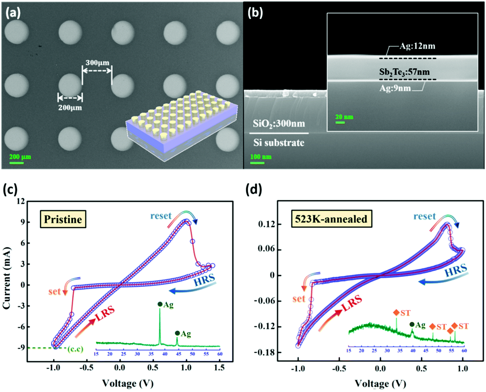 | ||
| Fig. 1 (a) Field-emission scanning electron microscopy (FESEM) images of the as-fabricated pillared Ag/Sb2Te3/Ag arrays on the SiO2/Si substrate from the top view. A schematic is inserted. (b) The magnified single cell from the side view. Typical current versus voltage (I–V) curves in (c) amorphous and (d) crystalline state cells with sweeping sequence arrows (0.2 s per cycle). The compliance current (Ic) of 9 mA is used to prevent the breakdown of the cell. XRD patterns of the corresponding cell are inserted with Ag diffraction peaks and Sb2Te3 (ST) diffraction peaks. | ||
In MIM memristors based on the electrochemical filament mechanism, an electroforming pulse that advances along ionic migration paths before bistable switching is usually achieved. However, the as-deposited amorphous Ag/Sb2Te3/Ag (a-ST) cells exhibit asymmetrical bipolar switching characteristics without any electroforming process (Fig. 1c). During the sweep from zero to a negative set voltage (Vset), the a-ST cell switches from high-resistance state (HRS) to low-resistance state (LRS). In the subsequent sweep, the operation is governed by a positive voltage bias and the a-ST cell sustains LRS until reaching the reset voltage (Vreset). The sharp set and reset switching are triggered in the I–V hysteresis, where Va-set = −0.7 V and Va-reset = 1 V. Interestingly, similar bipolar switching behaviors can be observed in c-ST cells with symmetrical Vc-set (−0.7 V) and Vc-reset (0.7 V), which is in contrast to the asymmetry hysteresis of a-ST cells with resistance variation.
The bipolar switching behaviors in chalcogenide-based MIM configuration are generally suggested to be originating from the phase transition. However, at a sufficiently high voltage bias, the I–V curves of the a-ST cells remain reversible and smooth with long operating time (Fig. S2 in the ESI†), which indicates that the phase transition of Sb2Te3 caused by Joule heat does not occur. Until now, a large variety of physical effects are known, which can, in principle, lead to resistive switching phenomena. Different mechanisms of resistive switching may be triggered in different material systems. Thus, further investigations on novel memristive behaviors of both a-ST and c-ST cells are significantly essential.
To prevent Sb2Te3-based heterojunctions from rapid heating or cooling, noncontact optical investigation was performed to characterize the microconductive properties. Using an in situ laser probe, the c-ST cells are characterized at LRS and HRS via photoluminescence and Raman spectra. As shown in Fig. 2a, the PL exciton peak for LRS is observed at the wavelength of 879 nm. Three extrinsic sub-absorption peaks at 622 nm, 716 nm and 791 nm are attributed to surface composite bonding between Ag and Sb2Te3, which was confirmed by the corresponding Raman analyses (Fig. S3 in the ESI†). In order to directly explore the local structural changes at the Ag/Sb2Te3 interfaces, research efforts were focused on Ag–Ag, Sb–Te, and Ag–Te interaction, as shown in Fig. 2b. Three main bands of Sb–Te vibration appeared at 76 cm−1, 84 cm−1 and 116 cm−1.26–28 Additional bands centered at 92 cm−1, 108 cm−1 and 153 cm−1 are attributed to the Ag electrode layer and the silver telluride interfacial compound. Interestingly, when transitioned to HRS, the PL excitonic peak shifted to 672 nm, as demonstrated in Fig. 2c. Taking into consideration the optical band-gap of Sb2Te3 (1.64 eV) (Fig. S4, ESI†), the main PL peak is blue-shifted by 0.21 eV at HRS and red-shifted by 0.23 eV at LRS (Fig. 3a). Since optical excitation peaks are positively correlated with electronic resonance and band structure, these shifts that behave symmetrically with the polarization of electric sweeping imply the movement of electronic band in Sb2Te3.29 However, no distinct changes in Raman peaks are observed at HRS except a slight frequency variation within 2 cm−1. Hence, bipolar switching in a single hysteresis is convincing with no structural phase transition in Ag/Sb2Te3/Ag memories. Such slight changes indicate local structural modulation during the switching process. As full width at half maximum (FWHM) of the Raman peaks can quantitatively reflect the corresponding bonding strength, the local structural modulation can be attributed to the changes in the interfacial bonding environment, as analyzed in Fig. 3b.30 The FWHM of Sb–Te peaks decreases at HRS, while Ag–Te bonding is comparably strengthened. The space charging barrier between Ag and Sb2Te3 is broadened with an intensifying sweeping voltage, and the local Sb–Te bonding is suppressed at the interfaces, thus possibly facilitating the built-in Schottky junction, as confirmed in Fig. S5 (ESI†).
 | ||
| Fig. 2 (a) PL spectrum and (b) Raman spectrum of Ag/c-ST/Ag heterojunctions at LRS, de-convolved into the Gaussian bands. (c) PL spectrum and (d) Raman spectrum at HRS with the Gaussian bands. Yellow color indicates the Raman peaks attributed to Sb–Te vibration, while green color indicates Ag peak and blue color indicates Ag–Te interface. | ||
 | ||
| Fig. 3 (a) Shift of PL peaks at LRS and HRS in Ag/c-ST/Ag heterojunctions, compared with an intrinsic optical band-gap of 1.64 eV. (b) Normalized FWHM of Raman peaks for Sb–Te, Ag–Ag, and Ag–Te vibration modes at LRS and HRS. | ||
To further clarify the underlying memristive mechanism, the electronic properties of Sb2Te3 were studied using first-principles calculations. Sb2Te3 is a p-type semiconductor with a narrow direct gap of 180 meV (Fig. 4a). From partial charge densities shown in Fig. 4b, it can be observed that Te-5p and Sb-5s contribute the valence band maximum (VBM), while the conductive band minimum (CBM) is dominated by p-orbital electrons of the Sb atoms. Since the electronegativity of Te is higher than that of Sb (4.85 eV for Sb, 5.49 eV for Te), Te loses electrons much easily.14 As shown in the Raman spectrum, Ag–Te bonding is generated as a space charge layer at interfaces when imposing low voltage. Through inducing higher electric stress on Sb2Te3, the conductive band moves downwards. As clearly demonstrated in Fig. 4c and d, the band-gap of Sb2Te3 follows the same trend as the red-shift of the PL peak. Accordingly, the Ag–Te bonding strengthens and space charge interfaces broadens, which is experimentally confirmed by an increase in the FWHM of Ag–Te Raman peaks at HRS. Moreover, the Fermi level of Sb2Te3 rises sensitively with the increase in external electric field. Due to the Fermi level pinning effect, the potential barrier height at interfaces should be strongly modulated by the movement of Fermi level, directly controlling the electron transportation behaviors in the Ag/c-ST/Ag heterojunction.31,32
 | ||
| Fig. 4 (a) Band structure of bulk Sb2Te3 with a narrow direct gap of 0.18 eV at gamma point. The green dot indicates VBM and the red dot indicates CBM. (b) Partial charge density of VBM and CBM. (c) Band structure of 3QL Sb2Te3 slab with the increase in perpendicular external electric field of 0 V Å−1, 0.05 V Å−1, 0.1 V Å−1, 0.15 V Å−1, 0.2 V Å−1 and 0.4 V Å−1, respectively. The green dot indicates VBM and the red dot indicates CBM. (d) Band gap and the Fermi level of 3QL Sb2Te3 slab as a function of perpendicular external electric field. | ||
Based on experimental indications and theoretical efforts, the schematic insight into the switchable process of Ag/Sb2Te3/Ag devices is illustrated in Fig. 5a. At the junction of a semiconductor and a metal, the bands of the semiconductor are pinned to the metal's Fermi level, which is an effect known as the Fermi level pinning effect.33Fig. 5a shows the initial band diagram of Ag/Sb2Te3/Ag hetero-structures under equilibrium state. When imposing a low positive bias from the left Ag electrode to the right Ag electrode, band bending varies at the interfaces: downward bending at the left Ag/Sb2Te3 contact with major carrier depletion, and upward bending at the other Sb2Te3/Ag contact with carrier accumulation.34 The degree of band bending depends on the Fermi movement of Sb2Te3 and carrier concentrations at surfaces, which should be in positive correlation with the external electric field. Under successive operations, intensifying the electric field prompts the rise of the Fermi level in Sb2Te3. Ohmic contact is gradually inverted to the built-in Schottky junction, as indicated in Fig. 5c. With the increase in barrier heights at both sides, carrier transportation, in turn, is blocked. The resistance of the memory cell suddenly increases. Then, the cell reaches HRS. The equivalent circuit of HRS resembles a head-to-head rectifier, which consists of two anti-serially connected diodes (DT and DB). Symmetrically, when the polarity of voltage is reversed, the Fermi level of Sb2Te3 shifts oppositely and the barrier height decreases. Once carrier energy overcomes the built-in barrier, recombination between electrons and holes at interfaces is gradually accelerated. Thus, HRS is reversed to LRS.
 | ||
| Fig. 5 Schematic of conductive Ag/Sb2Te3/Ag heterojunctions with interfacial barrier formation and carrier transportation (a) under equilibrium state, (b) under positive bias (V < Vreset), and (c) under positive bias (V ≫ Vreset) during the memristive process. The equivalent circuits are inserted. | ||
Thus, the movement of the electronic band in Sb2Te3 and transformation of the interfacial electron injection junctions possibly facilitate the reversible resistance switching in Ag/Sb2Te3/Ag devices. Direct observations exactly support the dynamic picture of memristive mechanisms in Ag/Sb2Te3/Ag heterocells and signify the role of the interfacial barrier in such resistive switching processes. Moreover, it is well known that investigations on the amorphous phase of Sb2Te3 remain challenging for both experimentalists and theorists. To simplify and optimize the research model, the detailed investigation on c-ST heterojunction was performed in the present study, and it would be much heuristic for memristive behaviors of amorphous Sb2Te3 in future investigations.
According to the above-mentioned discussions, a natural question arises as to whether the formation of fascinating multiple resistance states by combining phase transition is possible. In this contribution, independent memristive behaviors of a-ST and c-ST cells were generated together through thermal treatment, as shown in Fig. 6a. In order to verify the stability of the switches, a-ST and c-ST cells were individually characterized between HRS/LRS with a write/read voltage pulse. As indicated in Fig. 6b, four distinguished resistance values can be potentially achieved based on Ag/Sb2Te3/Ag hetero-structures by combining memristive capacities and thermal phase transition, so as to implement a novel multilevel memory concept. By applying 0.2 V read voltage, at least 101 resolution ratios between each resistance level and up to 5-order magnitude ranges of resistance capacity windows were significantly studied under 100 switching cycles. Compared with Sb2Te3-based phase change memory,35,36 the set, reset and read voltages of the resistive switching cells were much lower. The unique multi-level memory concept that generates nano-conductive mechanisms and high-density switches with low read/write voltage operation further qualifies Ag/Sb2Te3/Ag hetero-structures for large-area integration as memory devices. Although the retention tests were not investigated because the main purpose of the present studies was to explore the switchable conductive mechanism in Sb2Te3-based hetero-cells, the retention time might be efficiently enhanced by lower operating power that protects memories from electrical and thermal damage in actual storage applications. This should be an important task in the future.
 | ||
| Fig. 6 (a) I–V bipolar curves in the semi-logarithmic coordinate of the Ag/Sb2Te3/Ag hetero-structure that generates two pairs of resistance states of amorphous/crystalline phases. (b) Four electrical resistance levels of a-HRS, a-LRS, c-HRS and c-LRS at 0.2 V for 100 endurance cycles, which is individually investigated on amorphous and crystalline Ag/Sb2Te3/Ag hetero-structures. | ||
4. Conclusions
We successfully exploited the unique resistive switching behaviors of Ag/Sb2Te3/Ag heterocells that can be independently obtained in crystalline/amorphous phases. Each of the bipolar switches is not triggered by structural phase transition of Sb2Te3. In situ spectroscopic indications of Ag/Sb2Te3/Ag cells reveal that the origin of the electro-switching process possibly results from the electronic band movement of Sb2Te3. Theoretical studies, based on first-principles calculations, confirm that the valence changes and the Fermi level moves in Sb2Te3 with the increase in external electric field, giving rise to the Schottky–Ohmic barrier transformation and the sharp conductivity variation between HRS/LRS as a memristive mechanism. Combining resistance switches and phase transition in Ag/Sb2Te3/Ag hetero-structures, 4 resistance states with up to 5-order magnitude ranges of large resistance windows were investigated at low read voltage (∼0.2 V) by utilizing a novel multilevel memory potential for future scalable devices. These significant insights as well as the characterization of resistive switching nature should be further heuristic for technological implementation of chalcogenide-based memory devices.Author contributions
The manuscript was written through contributions of all authors. All authors have given approval to the final version of the manuscript.Conflicts of interest
There are no conflicts to declare.Acknowledgements
This work was supported by the Natural Science Foundation of Shanghai (17ZR1402200, 13ZR1402600), the National Natural Science Foundation of China (60578047, 61427815) and the Major State Basic Research Development Program of China (2009CB929201, 2012CB934303).References
- R. Waser and M. Aono, Nat. Mater., 2007, 6, 833 CrossRef PubMed.
- T. Tuma, A. Pantazi, M. Le Gallo, A. Sebastian and E. Eleftheriou, Nat. Nanotechnol., 2016, 11, 693–699 CrossRef PubMed.
- H. Steinberg, D. R. Gardner, Y. S. Lee and P. Jarillo-Herrero, Nano Lett., 2010, 10, 5032–5036 CrossRef PubMed.
- J. J. Yang, D. B. Strukov and D. R. Stewart, Nat. Nanotechnol., 2012, 8, 13–24 CrossRef PubMed.
- S. Yoo, T. Eom, T. Gwon and C. S. Hwang, Nanoscale, 2015, 7, 6340 RSC.
- X. Zhou, L. Wu, Z. Song, F. Rao, Y. Cheng, C. Peng, D. Yao, S. Song, B. Liu, S. Feng and B. Chen, Appl. Phys. Lett., 2011, 99, 2009–2012 Search PubMed.
- J. Jang, F. Pan, K. Braam and V. Subramanian, Adv. Mater., 2012, 24, 3573–3576 CrossRef PubMed.
- Y. Jung, S. H. Lee, A. T. Jennings and R. Agarwal, Nano Lett., 2008, 8, 2056–2062 CrossRef PubMed.
- D. Lencer, M. Salinga, B. Grabowski, T. Hickel, J. Neugebauer and M. Wuttig, Nat. Mater., 2008, 7, 972–977 CrossRef PubMed.
- B. Gholipour, J. Zhang, K. F. MacDonald, D. W. Hewak and N. I. Zheludev, Adv. Mater., 2013, 25, 3050–3054 CrossRef PubMed.
- M. Kim, C. H. Kim, H.-S. Kim and J. Ihm, Proc. Natl. Acad. Sci. U. S. A., 2012, 109, 671–674 CrossRef PubMed.
- D. Shakhvorostov, R. A. Nistor, L. Krusin-elbaum, G. J. Martyna, D. M. Newns, B. G. Elmegreen, X. Liu, Z. E. Hughes, S. Paul, C. Cabral and S. Raoux, Proc. Natl. Acad. Sci. U. S. A., 2009, 106, 10907–10911 CrossRef PubMed.
- A. Geresdi, M. Csontos, A. Gubicza, A. Halbritter and G. Mihály, Nanoscale, 2014, 6, 2613–2617 RSC.
- J. Y. Lee, J. H. Kim, D. J. Jeon, J. Han and J. S. Yeo, Nano Lett., 2016, 16, 6078–6085 CrossRef PubMed.
- A. V. Kolobov, P. Fons and J. Tominaga, Sci. Rep., 2015, 5, 13698 CrossRef PubMed.
- J. Momand, R. Wang, J. E. Boschker, M. A. Verheijen, R. Calarco and B. J. Kooi, Nanoscale, 2015, 7, 19136–19143 RSC.
- N. Ciocchini, M. Laudato, M. Boniardi, E. Varesi, P. Fantini, A. L. Lacaita and D. Ielmini, Sci. Rep., 2016, 6, 29162 CrossRef PubMed.
- C. Ahn, S. W. Fong, Y. Kim, S. Lee, A. Sood, C. M. Neumann, M. Asheghi, K. E. Goodson, E. Pop and H. S. P. Wong, Nano Lett., 2015, 15, 6809–6814 CrossRef PubMed.
- S. Tappertzhofen and S. Hofmann, Nanoscale, 2017, 17494–17504 RSC.
- R. Waser, R. Dittmann, C. Staikov and K. Szot, Adv. Mater., 2009, 21, 2632–2663 CrossRef.
- N. Han, M. U. Park and K. H. Yoo, ACS Appl. Mater. Interfaces, 2016, 8, 9224–9230 Search PubMed.
- B. Arndt, F. Borgatti, F. Offi, M. Phillips, P. Parreira, T. Meiners, S. Menzel, K. Skaja, G. Panaccione, D. A. Maclaren, R. Waser and R. Dittmann, Adv. Funct. Mater., 2017, 27, 1702282 CrossRef.
- J. J. Yang, M. D. Pickett, X. Li, D. A. A. Ohlberg, D. R. Stewart and R. S. Williams, Nat. Nanotechnol., 2008, 3, 429–433 CrossRef PubMed.
- T. Siegrist, P. Jost, H. Volker, M. Woda, P. Merkelbach, C. Schlockermann and M. Wuttig, Nat. Mater., 2011, 10, 202 CrossRef PubMed.
- L. Cario, C. Vaju, B. Corraze, V. Guiot and E. Janod, Adv. Mater., 2010, 22, 5193–5197 CrossRef PubMed.
- G. C. Sosso, S. Caravati and M. Bernasconi, J. Phys.: Condens. Matter, 2009, 21, 095410 CrossRef PubMed.
- J. Secor, M. A. Harris, L. Zhao, H. Deng, S. Raoux and L. Krusin-Elbaum, Appl. Phys. Lett., 2014, 104, 221908 CrossRef.
- X. Wang, K. Kunc, I. Loa, U. Schwarz and K. Syassen, Phys. Rev. B: Condens. Matter Mater. Phys., 2006, 74, 1–10 Search PubMed.
- S.-L. Li, K. Tsukagoshi, E. Orgiu and P. Samorì, Chem. Soc. Rev., 2015, 45, 118 RSC.
- A. K. U. Michel, D. N. Chigrin, T. W. W. Maß, K. Schönauer, M. Salinga, M. Wuttig and T. Taubner, Nano Lett., 2013, 13, 3470–3475 CrossRef PubMed.
- Y. Zhang, M. Snedaker, C. Birkel, S. Mubeen, X. Ji, Y. Shi and D. Liu, Nano Lett., 2012, 12, 1075–1080 CrossRef PubMed.
- Y. Zhang and G. D. Stucky, Chem. Mater., 2014, 26, 837–848 CrossRef.
- Z. Wu, X. Chen, Y. Zhang, C. Dun, D. L. Carroll and Z. Hu, Adv. Mater. Interfaces, 2018, 5, 1701210 CrossRef.
- T. You, N. Du, S. Slesazeck, T. Mikolajick, G. Li, D. Bürger, I. Skorupa, H. Stöcker, B. Abendroth, A. Beyer, K. Volz, O. G. Schmidt and H. Schmidt, ACS Appl. Mater. Interfaces, 2014, 6, 19758–19765 Search PubMed.
- C. Peng, L. Wu, Z. Song, F. Rao, M. Zhu, X. Li, B. Liu, L. Cheng, S. Feng, P. Yang and J. Chu, Appl. Surf. Sci., 2011, 257, 10667–10670 CrossRef.
- J. W. Park, S. H. Baek, T. D. Kang, H. Lee, Y. S. Kang, T. Y. Lee, D. S. Suh, K. J. Kim, C. K. Kim, Y. H. Khang, J. L. F. Da Silva and S. H. Wei, Appl. Phys. Lett., 2008, 93, 3–6 Search PubMed.
Footnote |
| † Electronic supplementary information (ESI) available. See DOI: 10.1039/c8cp00901e |
| This journal is © the Owner Societies 2018 |