
 Open Access Article
 This Open Access Article is licensed under a
 Creative Commons Attribution 3.0 Unported Licence
Band bending and dipole effect at interface of metal-nanoparticles and TiO2 directly observed by angular-resolved hard X-ray photoemission spectroscopy†
Shunsuke
Sato
 *a,
Keita
Kataoka
a,
Ryosuke
Jinnouchi
a,
Naoko
Takahashi
a,
Keita
Sekizawa
a,
Kousuke
Kitazumi
a,
Eiji
Ikenaga
bc,
Ryoji
Asahi
a and
Takeshi
Morikawa
*a
*a,
Keita
Kataoka
a,
Ryosuke
Jinnouchi
a,
Naoko
Takahashi
a,
Keita
Sekizawa
a,
Kousuke
Kitazumi
a,
Eiji
Ikenaga
bc,
Ryoji
Asahi
a and
Takeshi
Morikawa
*a
aToyota Central Research and Development Laboratories, Inc., Nagakute, Aichi 480-1192, Japan. E-mail: ssato@mosk.tytlabs.co.jp; morikawa@mosk.tytlabs.co.jp
bJASRI, SPring-8, Hyogo, 679-5198, Japan
cInstitute of Materials and Systems for Sustainability (IMaSS), Nagoya University, Furo-cho, Chikusa-ku, Nagoya, Aichi 464-8601, Japan
First published on 3rd April 2018
Abstract
This paper describes the observation of band bending and band edge shifts at the interfaces between nanoscale metals and TiO2 film over a wide depth range by angular-resolved hard X-ray photoemission spectroscopy (HAXPES). The HAXPES results indicate strong electrostatic interactions between the TiO2 semiconductor and metal nanoparticles, while density functional theory (DFT) calculations suggest that these interactions are primarily associated with charge transfer leading to electric dipole moments at the interface in the ground state. The effects of these dipole moments are not limited to the surface but also occur deep in the bulk of the semiconductor, and are highly dependent on the coverage of the metal nanoparticles on the semiconductor species.
Introduction
Photocatalytic and photoelectrochemical reactions using semiconductor materials have attracted a great deal of attention due to their potential uses in environmental remediation,1,2 water splitting3–9 and artificial photosynthesis systems10 utilizing solar radiation. It is well-known that photocatalytic activity is improved by the surface adsorption of metal or metal oxide co-catalysts.11,12 As an example, volatile organic compounds (VOCs) are decomposed by photo-excited TiO2, and this decomposition is accelerated by surface loading with nanoscale Pt (to form Pt/TiO2).1,11 Pt/TiO2 can also be used to split water for the stoichiometric production of hydrogen and oxygen under ultraviolet light.13 In this case, a nanoscale Pt co-catalyst attached to the TiO2 plays a significant role in improving reaction rates. Time-resolved transient spectroscopy has demonstrated very fast electron transfer from TiO2 in the photoexcited state to Pt (on the picosecond to nanosecond time scale).14 Although nanoscale Pt functions as an effective co-catalyst for TiO2, it is not universal and can be applied to limited number of semiconductors. As an example, Pt does not enhance photocatalytic H2 production from water-splitting over semiconductor photocatalysts such as TaON, Ta3N515 and LaTiO2N.16 Electron transfer from the semiconductor to the Pt proceeds relatively slowly over Pt-loaded LaTiO2N photocatalysts,16 and so hydrogen evolution is not improved by Pt loading. Such results suggest that variations in photocatalytic activity stem from differences in the electronic states of both the nanoscale co-catalysts and the semiconductors following the formation of metal–semiconductor junctions. Because this phenomenon has not been clarified experimentally, researchers currently select metal co-catalysts based on empirical evidence and their best judgment. Understanding the mechanisms associated with various co-catalyst/semiconductor combinations would therefore be truly useful with regard to photocatalyst design. Measurement of their electronic interaction of semiconductor films as they are active photocatalysts is important.The present report describes direct observations of band bending near the surfaces of film composed of bare TiO2 as well as films containing various nanoscale metals, using angular-resolved hard X-ray photoemission spectroscopy (HAXPES). Non-destructive HAXPES in conjunction with a wide angular resolution and intense irradiation at the SPring-8 (Super Photon ring-8 GeV) synchrotron radiation facility in Hyogo, Japan, has shown that loading of nanoscale metals on the semiconductor surface changes the electronic state of the semiconductor. Using this technique, electronic interactions have been observed not only at the semiconductor surface but also in the bulk of the TiO2. As such, both band bending and band potential shifts were identified both at the surface and in the bulk at depths as far as 35 nm (X-ray energy dependent). Based on DFT calculation results, it is clarified that the interaction is caused by electronic dipole moments from nanoscale metals to TiO2. This interaction may be important with regard to understanding and controlling photo-excited electron transfer from the semiconductors to the attached nanoscale metals because electron transfer rate is depended on the electronic coupling between donor and accepter.
Experimental
TiO2 films with thicknesses of approximately 200 nm were prepared on glass substrates coated with antimony-doped tin oxide (ATO) or fluorine-doped tin oxide (FTO), acting as transparent conductive oxides, by magnetron sputtering of a TiO2 target in a plasma composed of an Ar/O2 (4![[thin space (1/6-em)]](https://www.rsc.org/images/entities/char_2009.gif) :1 v/v) gas, followed by annealing at 723 K under an O2 gas flow for 2 h. Crystalline structure of TiO2 film was anatase.2 N-Doped Ta2O5(N-Ta2O5) films were prepared on ATO-coated glass substrates by reactive sputtering of Ta2O5 under various N2/Ar gas mixtures, followed by annealing at 873 K under a N2 gas flow for 2 h.17 Pt, Rh or Au nanoparticles were loaded onto these semiconductor films by RF magnetron sputtering, adjusting the amount of metal deposited to obtain a thickness of 1 nm. These semiconductor films synthesized with the same condition have already been reported to be active photocatalysts.18,19
:1 v/v) gas, followed by annealing at 723 K under an O2 gas flow for 2 h. Crystalline structure of TiO2 film was anatase.2 N-Doped Ta2O5(N-Ta2O5) films were prepared on ATO-coated glass substrates by reactive sputtering of Ta2O5 under various N2/Ar gas mixtures, followed by annealing at 873 K under a N2 gas flow for 2 h.17 Pt, Rh or Au nanoparticles were loaded onto these semiconductor films by RF magnetron sputtering, adjusting the amount of metal deposited to obtain a thickness of 1 nm. These semiconductor films synthesized with the same condition have already been reported to be active photocatalysts.18,19
The Ti 2p3/2 core levels were determined by XPS (Quantera SXM, Ulvac-Phi) with monochromatic Al Kα radiation. The angular-resolved HAXPES measurements were conducted on the SPring-8 BL47XU beamline using a photon energy of 7940 eV.20 The energies and angular distributions of the photoelectrons were assessed using a VG-Scienta R4000-HV hemispherical analyzer with an objective lens having an effective acceptance angle of approximately ±30° and an angular resolution of 1.32°. The stability of the system was confirmed using the Au 4f7/2 photoelectron peak for a Au film on a Si substrate, and the overall stability of the photoelectron energy was found to be within 50 meV. The angular distributions of the photoelectrons were determined at photoelectron take-off angles from 10° to 70° (with a take-off angle perpendicular to the surface defined as 90°). The analysis depths of the HAXPES measurements were calculated according to a previously reported procedure.21
Results and discussion
Angular-resolved HAXPES of TiO2 film
TiO2 film was prepared on antimony-doped tin oxide (ATO) or fluorine-doped tin oxide (FTO)-coated glass substrates by sputtering, following previously reported procedures.1 ATO- and FTO-coated substrates were employed to avoid charge-up during the HAXPES measurements. Analyses confirmed that TiO2 exhibits n-type properties together with an anatase crystalline structure. Sizes of the nanoscale Pt, Au and Rh particles deposited onto TiO2 film with a nominal thickness of 1 nm were determined to be 3–4 nm (Rh), 5–6 nm (Pt) and 10–15 nm (Au) based on transmission electron microscopy (TEM, Fig. S1, ESI†). The particles were confirmed to be metallic by both X-ray photoelectron spectroscopy (XPS) and HAXPES analyses. Fig. S2 (ESI†) summarizes the rates of photocatalytic hydrogen production over these films in 10% MeOH solution. The hydrogen production rates over both TiO2 (as a photocatalyst) was evidently improved by loading with these nanoscale metal co-catalyst as was previously reported.11 The effect of the Pt co-catalyst is seen to be highly dependent on the semiconductor, as is sometimes observed in semiconductor photocatalysts.15,16 In order to obtain a better understanding of the compatibility of these various materials, angular-resolved HAXPES (SPring-8, hν = 7.94 keV) was employed to analyze the chemical states at the semiconductor surface as well as band bending at various depths in the bulk semiconductor.The core-level spectra of bare semiconductors and semiconductors with attached nanoscale metals were acquired using angular-resolved HAXPES at take-off angles of 10 to 70°, with each spectrum obtained three or more times to ensure reproducibility. Selected HAXPES spectra are presented in Fig. 1, and the overall results are summarized in Fig. S3 (ESI†). Fig. 1 shows the HAXPES spectra for Ti 2p3/2 core state photoemission. The spectra acquired for the bare TiO2 films at take-off angles of 65° (representing a bulk phase spectrum at a maximum analysis depth of approximately 31 nm) and 10° (representing a surface spectrum at a maximum analysis depth of approximately 6 nm) are similar, without any significant shifts.21 The carrier densities in these TiO2 films were determined to be approximately 6 × 1017 cm−3 by our previous report,18 a value that is sufficient to induce band bending. It should be noted that depletion layer in the present TiO2 (>100 nm) is deeper than this HAXPES measurement depth. Therefore, we discuss HAXPES data from surface to middle of the band bending, which is still much more informative than the XPS. This depth dependence of the energy shift in the HAXPES core levels is understood to indicate a band bending profile near the semiconductor surface.20,22–25 The bare TiO2 film did not exhibit a band bending profile. However, upon deposition of nanoscale Pt, the TiO2 film (Pt/TiO2) showed upward band bending by 0.07 eV, such that the binding energy peak near the surface (at a take-off angle of 10°) was at a higher energy position than that in the bulk (at a take-off angle of 65°). In addition, the Ti 2p3/2 peak position of bare TiO2 in the bulk (65°) was shifted negatively by 0.25 eV by the deposition of Pt (Pt/TiO2), as shown in Fig. 1. Furthermore, we confirmed that Ti 2p3/2 peaks broadened in the case of nanoscale metals. For example, full width at half maximum (FWHM) of TiO2 and Pt/TiO2 films were about 0.73 and 0.80 eV respectability. Such a peak (core level) broadening indicated that there is the band bending in Pt/TiO2 film.26
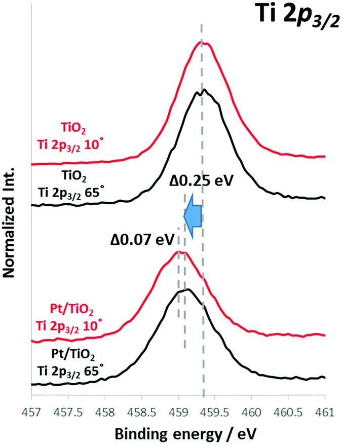 | ||
| Fig. 1 Ti 2p3/2 spectra acquired from TiO2 and Pt/TiO2 by angular-resolved HAXPES [at take-off angles of 10° (red lines) and 65° (black lines)]. | ||
Fig. 2 plots the take-off-angle dependence of the Ti 2p3/2 peak positions for TiO2 films with adsorbed nanoscale Pt, Au and Rh. The TiO2 film spectrum is nearly flat going from the bulk to the surface, while the TiO2 films with adsorbed nanoscale metals instead show upward band bending toward the surface, together with an overall upward shift. Typically, the degree and direction of band bending at metal/semiconductor junctions can be explained by the difference in work functions, using the Mott–Schottky model.25,27 The work functions for Pt, Au and Rh are 5.65, 5.1 and 4.9 eV,28 respectively, all of which are greater than that for TiO2 (4.5 eV). Therefore, upward band bending observed by the angular-resolved HAXPES were reasonable. However, peak shifts were also observed. For example, core level of Rh/TiO2 was about 0.3 eV lower than that of bare TiO2 film. According to a previous report,29 such core level shifts toward lower binding energy were observed by XPS under application of forward potentials. Because we have confirmed influence of charge-up of the samples were negligible as will be explained later, the observed peak shifts of the metal/TiO2 films are considered to be induced by strong interaction in the ground state. The present results suggest that nanoscale metal particles play a key role in the larger peak shift, indicating that a Fermi level shift25 was induced in the presence of nanoscale metal particles on the surface of the TiO2 as the result of strong interactions.
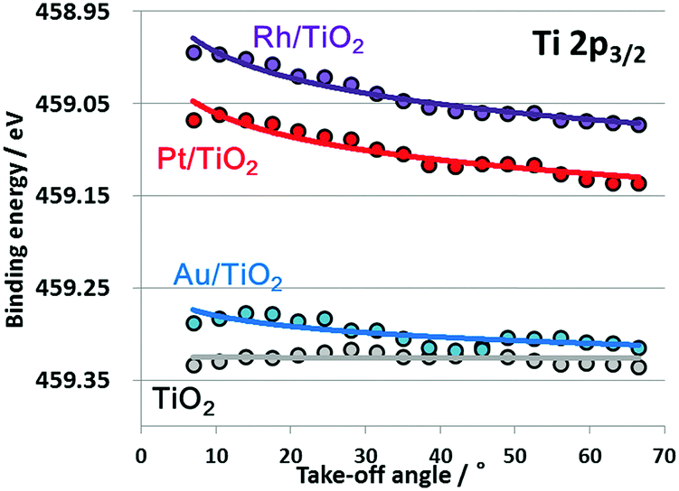 | ||
| Fig. 2 Shifts in peak positions relative to positions in angular spectrum for series of Ti 2p3/2 spectra obtained from TiO2, Au/TiO2, Pt/TiO2 and Rh/TiO2. | ||
Electrostatic interaction by dipole effect
The HAXPES results presented herein indicate strong interactions between the semiconductors and nanoscale metals in the ground state. As an example, the deposition of nanoscale Pt onto a TiO2 film caused a peak shift of 0.25 eV toward a lower binding energy along with upward band bending. A similar peak shift in XPS spectra has been discussed for nanoscale metal/semiconductors junctions such as Pt/TiO2, Au/TiO2, Pd/TiO2, Pt/ZnO, Ni/SiC, metal/GaN,30–36 and recently HAXPES was applied to a Ni/Al2O3/GaAs system.37 The shift in the core-level peak position for the metal/semiconductor combination originates from band bending toward the surface. However, in principle, XPS cannot distinguish band bending from this peak shift because this technique assesses chemical states only within a shallow surface region (2–3 nm in depth). The HAXPES data provided in previous reports originates only from a single point (acquired at a single take-off angle). In contrast, the angular-resolved HAXPES technique used in the present study (to a depth of approximately 35 nm) demonstrates that the peak shift is the result of band bending. As noted, spectra acquired at different incident photon fluxes (Fig. S4, ESI†) confirm that the peak shifts are also not the result of photovoltaic charging of the nanoscale metals.38,39 Thus, the observed peak shifts are attributed to electrostatic interactions between the nanoscale metals and semiconductors. We also confirmed that the band bending and the peak shift were also confirmed for other material with a different property, N-doped Ta2O5(N-Ta2O5), which exhibited cathodic photoresponse together with photocatalytic CO2 reduction and hydrogen generation reactions by surface addition of nanoscaled cocatalysts. In this case, an obvious downward band bending of 0.4 eV was observed from bulk to surface of the N-Ta2O5 film (Fig. S5, ESI†).17,19,40 Similar peak shifts have sometimes been discussed with regard to high-temperature thermal catalysis systems for the chemisorption of H2 and CO on metal particles via strong metal–support interactions (SMSI).41,42 The SMSI effect has largely been explained by the decoration model, which describes the encapsulation of the deposited metal by a thin oxide layer stemming from the support during annealing. However, the configurations of the present metal-adsorbed semiconductor films synthesized at ambient temperature differ from this model.A few previous studies using DFT calculations, electron spin resonance or Kelvin probe force microscopy have reported charge migration from nanoscale Pt particles to a semiconductor such as TiO2.43–45 According to these reports and our experimental results, the electrostatic interactions are greatly affected by the size of the nanoscale metal particles. As an example, 10 nm Rh deposition (a ten-fold greater thickness of Rh/TiO2) on TiO2 film (10 nm Rh/TiO2-film) reduces the extent of band bending compared to that observed for a Rh/TiO2 film (Fig. S6, ESI†). To understand the origin of such electrostatic interactions at the microscopic level, DFT calculations were performed to simulate the Ti 2p3/2 photoemission spectra of TiO2 films with attached nanoscale metals, with the results shown in Fig. 3 and Fig. S7–S9 (ESI†). Each of the Ti 2p3/2 peaks associated with TiO2 films incorporating metals were found to be shifted negatively from that for a bare TiO2 film (Fig. 3a). In addition, these DFT results confirm that the bond length between the Rh and Ti of Rh/TiO2 is comparable to the Rh–Rh bond length (that is, Rh–Ti bond lengths of 2.69 to 2.72 Å were obtained from DFT, while the Rh–Rh bond length is 2.70 Å). The largest negative shift seen in the DFT results was for TiO2 with twelve Rh atoms (Rh12/TiO2), while Rh/TiO2 exhibited the greatest negative shift of the Ti 2p3/2 peak among the metal/TiO2 films in the HAXPES spectra. Thus, these DFT calculations strongly support trend of direction and dependence of metal species of these shifts. The Au/TiO2 film showed the smallest negative shift of all the metal/TiO2 films, presumably due to the larger size of the Au particles compared to the other metals (Fig. S1, ESI†). These results also demonstrate that the calculated peak shift depends on both the shape and size of the metal particles. As an example, the Ti 2p3/2 binding energy peak for TiO2 adjacent to nanoscale metal particles undergoes a greater negative shift than that adjacent to thin metal films. These results also demonstrate that DFT calculations can explain quantitatively the dependence of charge transfer on the size of the metal particles as determined from the HAXPES data. Fig. 3b presents the calculated binding energies for the Ti 2p3/2 peaks as a function of the intensity of the charge transfer between TiO2 and the metals. It is notable that the Ti 2p3/2 binding energies for all metal particles fall on a single line, meaning that the negative Ti 2p3/2 peak shift is determined by the extent of the charge transfer from the nanoscale metal to the TiO2. This charge transfer results in a dipole moment at the interface and thus shifts the electrostatic potential. The most significant charge transfer among the metals was observed in the case of Rh particles on TiO2, while the least amount of transfer was associated with Au particles on TiO2. This difference in charge transfer may possibly be attributable to the ionization energy values for these metals; the lower ionization energy for metals such as Rh could increase the charge transfer in the vicinity of the oxygen in TiO2.
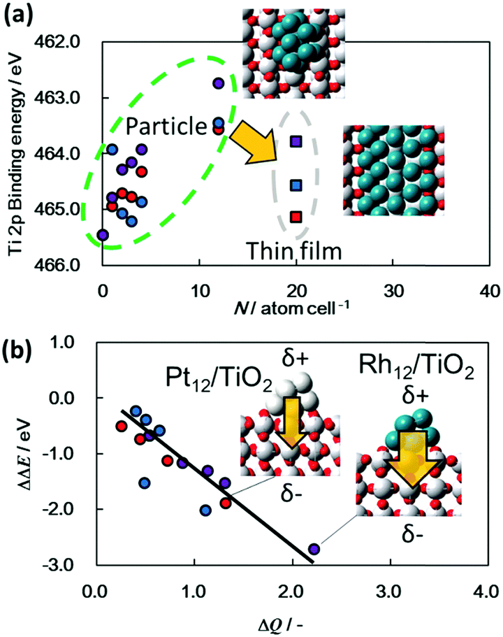 | ||
Fig. 3 (a) Binding energy values for the Ti 2p3/2 peaks for metal particles or thin films on TiO2 as calculated using DFT [red circles ( ): Pt particles on TiO2; blue circles ( ): Pt particles on TiO2; blue circles ( ): Au particles on TiO2; purple circles ( ): Au particles on TiO2; purple circles ( ): Rh particles on TiO2; red squares ( ): Rh particles on TiO2; red squares ( ): thin Pt film on TiO2; blue squares ( ): thin Pt film on TiO2; blue squares ( ): thin Au film on TiO2; purple squares ( ): thin Au film on TiO2; purple squares ( ): thin Rh film on TiO2], and (b) relationship between calculated Ti 2p3/2 peak binding energy values and charge transfer intensity (ΔQ) between metal particles and TiO2 films [red circles ( ): thin Rh film on TiO2], and (b) relationship between calculated Ti 2p3/2 peak binding energy values and charge transfer intensity (ΔQ) between metal particles and TiO2 films [red circles ( ): Pt particles on TiO2; blue circles ( ): Pt particles on TiO2; blue circles ( ): Au particles on TiO2; purple circles ( ): Au particles on TiO2; purple circles ( ): Rh particles on TiO2]. ): Rh particles on TiO2]. | ||
The present DFT calculations and experimental results, as well as previous reports,43–47 all are in agreement so far as they indicate that the peak shifts in the photoemission spectra of semiconductors attached to nanoscale metals can be explained by electrostatic interactions with associated dipole moments. This phenomenon affects both the surface and bulk properties of the semiconductors. Although there has been much research regarding the improvement of photocatalytic reactions by the loading of metal co-catalysts, there has been minimal discussion of the relationship between electronic interactions at the metal co-catalyst/semiconductor interface and photocatalysis, based on assessments of electronic states in the depth direction. Interestingly, several researchers have recently attempted to control the band positions for semiconductor films by making use of the dipole effect,48,49 and HAXPES analysis could contribute to a more detailed understanding of such studies.
Conclusions
In summary, this work demonstrated the direct observation of both band shifts and band bending between nanoscale metal particles (Pt, Au or Rh) and TiO2 using angular-resolved HAXPES. The results directly indicate the existence of electrostatic interactions between the nanoscale metals and semiconductors. DFT calculations suggest that the observed electrostatic interactions are associated with dipole effects and influence not only the surface but also the bulk properties of the semiconductors. Thus, the chemical nature between the nanoscale metal particle and the semiconductor can significantly influence the charge transfer from nanoscale metal followed by the photocatalytic reaction. Of course, the catalytic activities of semiconductor photocatalysts are affected by many other factors, including the orientations of crystal planes, size effects, surface area of co-catalysts and the density of lattice defects.50 The control of band potential of semiconductor is very important because band potential largely dominates semiconductor property, especially the charge transfer. Since the electronic ground states greatly dominate electron transfer in semiconductor devices, an understanding of these electronic states is crucial to the design of active photocatalysts, photoelectrodes and quantum dot solar cells.Conflicts of interest
There are no conflicts to declare.Acknowledgements
The authors thank K. Oishi for technical assistance. The HAXPES analyses were performed with the approval of the SPring-8 Program Advisory Committee (Proposal No. 2013A1014, 2013B1018 and 2014A1009). This work was supported in part by the Advanced Catalytic Transformation Program for Carbon Utilization (ACT-C, Grant Number JPMJCR12ZA) of the Japan Science and Technology Agency (JST).Notes and references
- M. R. Hoffmann, S. T. Martin, W. Choi and D. W. Bahnemann, Chem. Rev., 1995, 95, 69 CrossRef CAS.
- R. Asahi, T. Morikawa, T. Ohwaki, K. Aoki and Y. Taga, Science, 2001, 293, 269 CrossRef CAS PubMed.
- A. Fujishima and K. Honda, Nature, 1972, 238, 37 CrossRef CAS PubMed.
- K. Maeda, K. Teramura, D. Lu, T. Takata, N. Saito, Y. Inoue and K. Domen, Nature, 2006, 440, 295 CrossRef CAS PubMed.
- A. Iwase and A. Kudo, J. Mater. Chem., 2010, 20, 7536 RSC.
- R. Abe, K. Sayama and H. Arakawa, J. Photochem. Photobiol., A, 2004, 166, 115 CrossRef CAS.
- D. Wang, R. Li, J. Zhu, J. Shi, J. Han, J. X. Zong and C. Li, J. Phys. Chem. C, 2012, 116, 5082 CAS.
- F. F. Abdi, L. Han, A. H. Z. Smets, M. Zeman, B. Dam and R. van de Krol, Nat. Commun., 2013, 4, 2195 Search PubMed.
- D. M. Fabian, S. Hu, N. Singh, F. A. Houle, T. Hisatomi, K. Domen, F. E. Osterloh and S. Ardo, Energy Environ. Sci., 2015, 8, 2825 CAS.
- T. Arai, S. Sato and T. Morikawa, Energy Environ. Sci., 2015, 8, 1998 CAS.
- Y. Nosaka, K. Norimatsu and H. Miyama, Chem. Phys. Lett., 1984, 106, 128 CrossRef CAS.
- S. Higashimoto, W. Tanihata, Y. Nakagawa, M. Azuma, H. Ohue and Y. Sakata, Appl. Catal., A, 2008, 340, 98 CrossRef CAS.
- S. Sato and J. M. White, Chem. Phys. Lett., 1980, 72, 83 CrossRef CAS.
- A. Furube, T. Asahi, H. Masuhara, H. Yamashita and M. Anpo, J. Phys. Chem. B, 1990, 103, 3120 CrossRef.
- M. Hara, J. Nunoshige, T. Takata, J. N. Kondo and K. Domen, Chem. Commun., 2003, 3000 RSC.
- A. Yamakata, M. Kawaguchi, N. Nishimura, T. Minegishi, J. Kubota and K. Domen, J. Phys. Chem. C, 2014, 118, 23897 CAS.
- T. Morikawa, S. Saeki, T. M. Suzuki, T. Kajino and T. Motohiro, Appl. Phys. Lett., 2010, 96, 142111 CrossRef.
- Y. Nakano, T. Morikawa, T. Ohwaki and Y. Taga, Appl. Phys. Lett., 2005, 86, 132104 CrossRef.
- S. Sato, T. Morikawa, S. Saeki, T. Kajino and T. Motohiro, Angew. Chem., Int. Ed., 2010, 49, 5101 CrossRef CAS PubMed.
- E. Ikenaga, M. Kobata, H. Matsuda, T. Sugiyama, H. Daimon and K. Kobayashi, J. Electron Spectrosc. Relat. Phenom., 2013, 190, 180 CrossRef CAS.
- S. Tanuma, C. J. Powell and D. R. Penn, Surf. Interface Anal., 1988, 11, 577 CrossRef CAS.
- K. Kataoka, Y. Kimoto, K. Horibuchi, T. Nonaka, N. Takahashi, T. Narita, M. Kanechika and K. Dohmae, Surf. Interface Anal., 2012, 44, 709 CrossRef CAS.
- C. E. ViolBarbosa, C. Shekhar, B. Yan, S. Ouardi, E. Ikenaga, G. H. Fecher and C. Felser, Phys. Rev. B: Condens. Matter Mater. Phys., 2013, 88, 195128 CrossRef.
- M. Imura, S. Tsuda, T. Nagata, H. Takeda, M. Liao, A. Yang, Y. Yamashita, H. Yoshikawa, Y. Koide, K. Kobayashi, T. Yamaguchi, M. Kaneko, N. Uematsu, T. Araki and Y. Nanishi, J. Appl. Phys., 2013, 114, 033505 CrossRef.
- C. Weiland, A. K. Rumaiz and J. C. Woicik, in Hard X-Ray Photoelectron Spectroscopy (HAXPES), ed. J. C. Woicik, Springer, Heidelberg, 2016, p. 381 Search PubMed.
- C. Weiland, G. E. Sterbinsky, A. K. Rumaiz, C. S. Hellberg, J. C. Woicik, S. Zhu and D. G. Schlom, Phys. Rev. B: Condens. Matter Mater. Phys., 2015, 91, 165103 CrossRef.
- R. Tung, Mater. Sci. Eng., R, 2001, 35, 1 CrossRef.
- T. Mori, T. Kozawa, T. Ohwaki, Y. Taga, S. Nagai, S. Yamasaki, S. Asami, N. Shibata and M. Koike, Appl. Phys. Lett., 1996, 69, 3537 CrossRef CAS.
- H. Kobayashi, Y. Yamashita, K. Namba and Y. Nakano, Jpn. J. Appl. Phys., 1994, 33, L754 CrossRef CAS.
- S. Porsgaard, P. Jiang, F. Borondics, S. Wendt, Z. Liu, H. Bluhm, F. Besenbacher and M. Salmeron, Angew. Chem., Int. Ed., 2011, 50, 2266 CrossRef CAS PubMed.
- Z. Zhang and J. T. Yates, Jr., Chem. Rev., 2012, 112, 5520 CrossRef CAS PubMed.
- F. S. Roberts, S. L. Anderson, A. C. Reber and S. N. Khanna, J. Phys. Chem. C, 2015, 119, 6033 CAS.
- K. M. Tracy, P. J. Hartlieb, S. Einfeldt, R. F. Davis, E. H. Hurt and R. J. Nemanich, J. Appl. Phys., 2003, 94, 3939 CrossRef CAS.
- Y. Z. Yang, C.-H. Chang and H. Idriss, Appl. Catal., B, 2006, 67, 217 CrossRef CAS.
- T. Kim, M. Yoshitake, S. Yagyu, S. Nemsak, T. Nagata and T. Chikyow, Surf. Interface Anal., 2010, 42, 1528 CrossRef CAS.
- L. Adam, T. Laure, R. Agata and A.-V. Nicolas, J. Phys. Chem. C, 2011, 115, 20153 Search PubMed.
- A. Lee and G. H. Walsh, Phys. Rev. B: Condens. Matter Mater. Phys., 2013, 88, 045322 CrossRef.
- E. Mete, O. Gülseren and Ş. Ellialtıoğlu, Eur. Phys. J. B, 2012, 85, 204 CrossRef.
- A. Sasahara, C. L. Pang and H. Onishi, J. Phys. Chem. B, 2006, 110, 13453 CrossRef CAS PubMed.
- T. M. Suzuki, S. Saeki, K. Sekizawa, K. Kitazumi, N. Takahashi and T. Morikawa, Appl. Catal., B, 2017, 202, 597 CrossRef CAS.
- S. Bonanni, K. Aït-Mansour, H. Brune and W. Harbich, ACS Catal., 2011, 1, 385 CrossRef CAS.
- J. Ohyama, A. Yamamoto, K. Teramura, T. Shishido and T. Tanaka, ACS Catal., 2011, 1, 187 CrossRef CAS.
- T. M. Salama, H. Hattori, H. Kita, K. Ebitani and T. Tanaka, J. Chem. Soc., Faraday Trans., 1993, 89, 2067 RSC.
- M. H. Hecht, J. Vac. Sci. Technol., B, 1990, 8, 1018 CAS.
- K. Ozawa, M. Emori, S. Yamamoto, R. Yukawa, S. Yamamoto, R. Hobara, K. Fujikawa, H. Sakama and I. Matsuda, J. Phys. Chem. Lett., 2014, 5, 1953 CrossRef CAS PubMed.
- Y. Liu, S. R. Scully, M. D. McGehee, J. Liu, C. K. Luscombe, J. M. J. Fréchet, S. E. Shaheen and D. S. Ginley, J. Phys. Chem. B, 2006, 110, 3257 CrossRef CAS PubMed.
- K. Onda, L. Bin and P. Hrvoje, Phys. Rev. B: Condens. Matter Mater. Phys., 2004, 70, 045415 CrossRef.
- R. Jinnouchi, A. V. Akimov, S. Shirai, R. Asahi and O. V. Prezhdo, J. Phys. Chem. C, 2015, 119, 26925 CAS.
- Y. Hikita, K. Nishio, L. C. Seitz, P. Chakthranont, T. Tachikawa, T. F. Jaramillo and H. Y. Hwang, Adv. Energy Mater., 2016, 6, 1502154 CrossRef.
- O. O. P. Mahaney, N. Murakami, R. Abe and B. Ohtani, Chem. Lett., 2009, 38, 238 CrossRef.
Footnote |
| † Electronic supplementary information (ESI) available. See DOI: 10.1039/c8cp00551f |
| This journal is © the Owner Societies 2018 |