
Nucleation and growth of zinc crystals on a liquid surface
Chenxi
Lu
a,
Ying
Jin
a,
Xiangming
Tao
a,
Bo
Yang
a and
Gaoxiang
Ye
*ab
aDepartment of Physics, Zhejiang University, Hangzhou 310027, P. R. China. E-mail: gxye@zju.edu.cn; gxye@mail.hz.zj.cn
bDepartment of Physics, Zhejiang University of Science & Technology, Hangzhou 310023, P. R. China
First published on 20th November 2017
Abstract
A catalyst-free preparation method for zinc nanocrystals on a silicone oil surface is developed at room temperature. The growth tendency of one- and two-dimensional zinc crystals, which may be tunable by the deposition rate, can be attributed mainly to the preferential growth characteristics of the crystals. The formation of zinc crystal mounds with nanoscale steps results from both the preferential growth characteristics and strong step-edge barriers. A new aggregation mechanism involving competitive growth among the preferential growth directions is proposed.
Introduction
In the past decades, one-dimensional nanostructures,1,2 such as nanowires, nanorods, nanobelts, etc., have received steadily growing interest owing to their unique properties and promising applications in nanoscale devices. In particular, one-dimensional metal nanostructures,3,4 which are considered as possible interconnects or functional elements in future nanodevices, have also become the focus of intensive research studies.Nowadays, considerable attention is given to one-dimensional zinc (Zn) nanostructures for their applications in terms of superhydrophobic substrates,5 rechargeable electrical batteries,6 atmospheric corrosion-resistance materials,7etc. To date, electrochemical deposition8–10 and thermal evaporation11–13 are usually used to synthesize one-dimensional Zn nanostructures. For electrochemical deposition, post-synthesis device assembly may require removal of the template which may cause damage to the one-dimensional Zn nanostructures. Unfortunately, high substrate temperatures (150–350 °C) are usually needed to fabricate one-dimensional Zn nanostructures on solid substrates by thermal evaporation of Zn,11 ZnS,12 ZnO,13etc. From an industrial point of view, substrate heating increases the production cost, energy consumption and system complexity. Hence, a convenient and energy-saving approach to fabricate one-dimensional Zn nanostructures is desirable all the time.
Recently, one-dimensional Zn nanocrystals were prepared in a catalyst-free manner on a silicone oil surface at room temperature by thermal evaporation.14 It was verified that the one-dimensional Zn nanocrystals really grow along the preferential growth direction, i.e., the [001] direction of the Zn crystal. This experimental result indicates a new growth mechanism of the crystals on liquid surfaces.
In contrast, as ancillary products in most studies,15–17 two-dimensional Zn nanocrystals, namely Zn nanoplates, could also be one of the most important functional materials for nanodevices due to their superior electrochemical properties. Obviously, the study of controllable growth of the Zn nanocrystals in both size and morphology is pretty important.
On the other hand, layer-by-layer growth on an atomically two-dimensional terrace easily occurs due to the step-edge barrier for descending atoms in epitaxial growth.18–20 However, to our best knowledge, there are few reports on such a phenomenon on two-dimensional terraces with nanoscale steps.
Nowadays, many efforts have been made to find effective methods for preparing various nanocrystals, which should be simple, inexpensive and environmentally friendly.
In this paper, one- and two-dimensional Zn crystals, i.e., Zn nanowires, nanorods, nanobelts and polygonal nanoplates, are prepared in a catalyst-free manner on a silicone oil surface at room temperature by thermal evaporation. The aspect ratio, a characteristic parameter reflecting the tendency of one- or two-dimensional growth, may be tunable by the deposition rate. It is remarkable that the aspect ratio of the Zn crystals may be over 150 in our experiment. Besides, Zn mounds with nanoscale steps are also observed on the silicone oil surface. In order to explain these interesting phenomena, we propose a new aggregation mechanism, in which competitive growth among the preferential growth directions is involved.
Experimental
In our experiment, a commercial silicone oil (Dow Corning 705 diffusion pump fluid) with low vapor pressure (∼10−10 mbar) at room temperature was chosen as the liquid substrate, which was uniformly coated onto a 10 × 10 mm2 ground glass surface with a resulting film thickness of around 0.5 mm. For the sake of comparison, another piece of clean ground glass was used as a solid substrate. Zn crystals formed on both of the substrates by thermal evaporation of Zn (99.99+%, Alfa Aesar) in a vacuum of 2.0 × 10⁻⁶ mbar at room temperature (T = 20 ± 2 °C). A quartz crystal microbalance near the substrates monitored the nominal deposition rate f and Zn film thickness d.After deposition, the samples were kept in the evaporation chamber for 30 minutes. Then, the Zn crystals were transferred from the silicone oil surface to a polished single crystalline silicon wafer for observation using a scanning electron microscope (SEM, SUPRA 55) equipped with an energy-dispersive X-ray spectrometer (EDS).14 Probably, this transfer process may change the locations of the Zn crystals on the substrate, however, it hardly changed their morphologies and microstructures. The microstructures of the Zn crystals were analyzed using a transmission electron microscope (TEM, JEM-2010) after the preparation procedure as follows: (i) the sample was soaked in an acetone solution to separate the Zn crystals from the silicone oil surface; (ii) a copper grid with an ultrathin carbon film was used to collect the Zn crystals in/on the acetone solution; (iii) the copper grid covered with the Zn crystals was dried under an infrared oven lamp.
Results and discussion
Fig. 1 shows the morphologies of the Zn crystals grown on the substrates. On the clean ground glass surface, as shown in Fig. 1a, lots of scattered hexagonal Zn nanoplates can be observed and no other morphologies of the crystals are detected, which is consistent with the isotropic characteristics of the glass surface. The result shown in Fig. 1a is in agreement with previous findings.21,22 On the silicone oil surface, however, one-dimensional (or to be more exact, quasi-one-dimensional) Zn crystals accompanied by some polygonal Zn nanoplates are randomly distributed, as shown in Fig. 1b.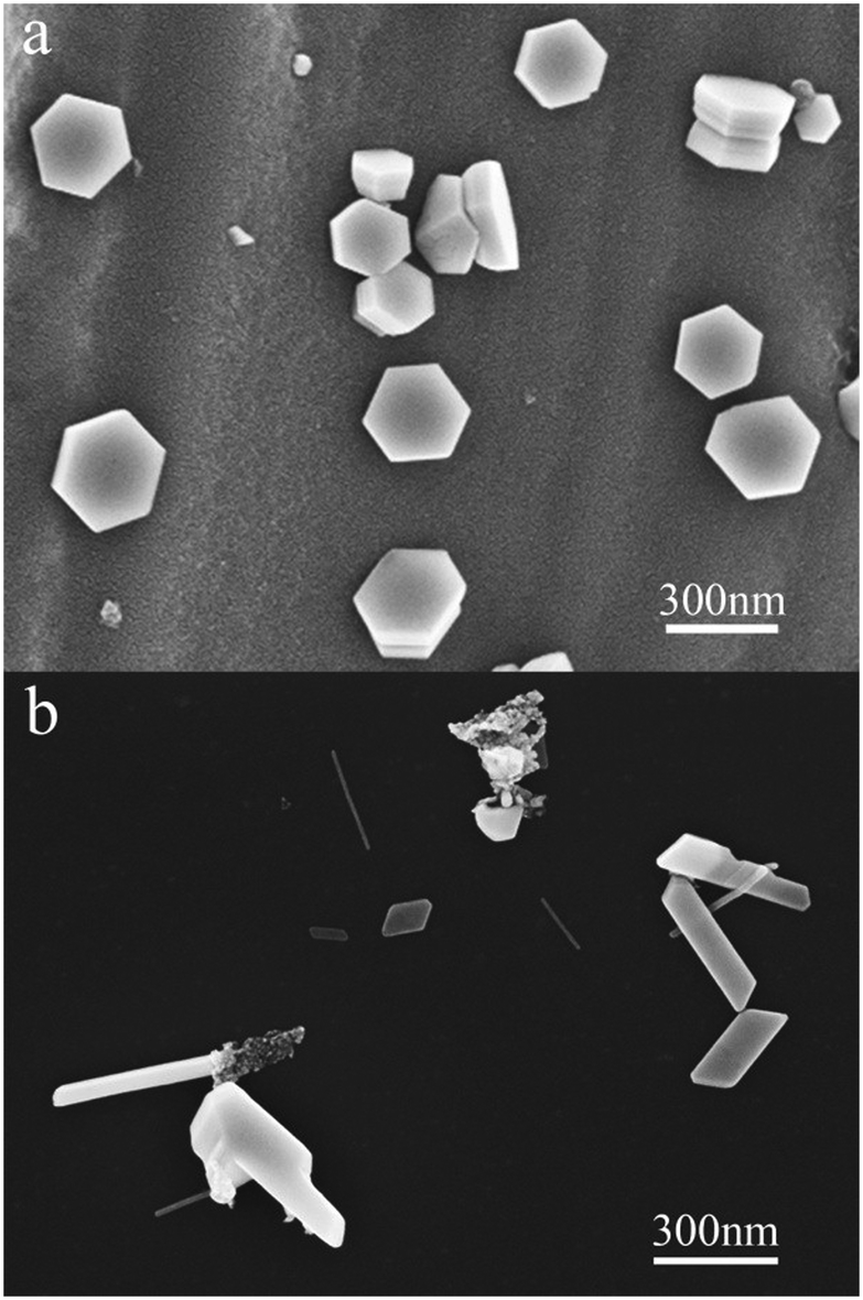 | ||
| Fig. 1 SEM images of the Zn crystals after deposition (f = 0.01 nm s−1, d = 8.0 nm). (a) On a clean ground glass surface. (b) On a silicone oil surface. | ||
Fig. 2 shows several characteristic morphologies of the one-dimensional Zn crystals grown on the silicone oil surface, such as nanowires, nanobelts, kinked nanorods, needle-like nanorods, straight nanorods, etc. It should be mentioned that, however, most of the one-dimensional Zn crystals (>95%) are uniform and straight nanorods in our experiment. Besides, the nanorods usually exhibit a corner angle of 120°, as shown in Fig. 2e and f. If we take a closer look at the photo in Fig. 2f, we can see that the cross-section of the nanorod looks like a rectangle. The morphologies shown in Fig. 2 indicate that the nanorods may exhibit a crystal structure.
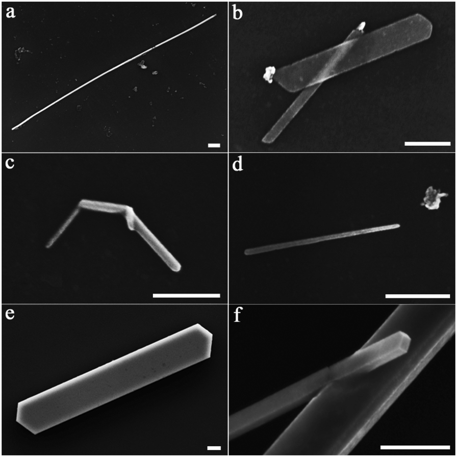 | ||
| Fig. 2 Morphologies of the one-dimensional Zn crystals grown on the silicone oil surface (f = 0.01 nm s−1, d = 8.0 nm). (a) Nanowire. (b) Nanobelts. (c) Kinked nanorod. (d) Needle-like nanorod. (e and f) Straight nanorods. Scale bars, 200 nm. | ||
Basically, the formation of the hexagonal Zn nanoplates on the clean ground glass surface may be attributed to the vapor–solid mechanism.23 However, the growth mechanism of the one-dimensional Zn crystals on the silicone oil surface is quite puzzling, since the oil surface is an isotropic and quasi-free sustained substrate. Moreover, it should be noticed that the growth process of the crystals shown in Fig. 1 and 2 is catalyst-free and therefore it should not be in the range of both the vapor–liquid–solid24 and the solution–liquid–solid25 mechanisms.
On one hand, the liquid surface possesses isotropic and quasi-free sustained characteristics, which may lead to random and free diffusion for all the deposition atoms on the two-dimensional surface.26,27 The mean square displacement of the deposition atoms is given by 〈Δr2〉 = 4DΔt, where D is the diffusion coefficient and Δt is the diffusion time.28–30
On the other hand, the Zn crystal possesses a hexagonal close-packed (hcp) crystal structure and the [001] and [010] directions turn out to be the preferential growth directions in vapor growth.31,32 We suggest that the isotropic and quasi-free sustained liquid substrates may facilitate this oriented growth phenomenon in comparison with the solid substrates.
An interesting phenomenon is that various Zn nanoplates with quadrangular, pentagonal and hexagonal morphologies, etc., together with the one-dimensional Zn crystals, may appear on the silicone oil surface, as shown in Fig. 1b and 3. This phenomenon has never been observed in the samples on the clean ground glass surface under similar experimental conditions (see Fig. 1a).
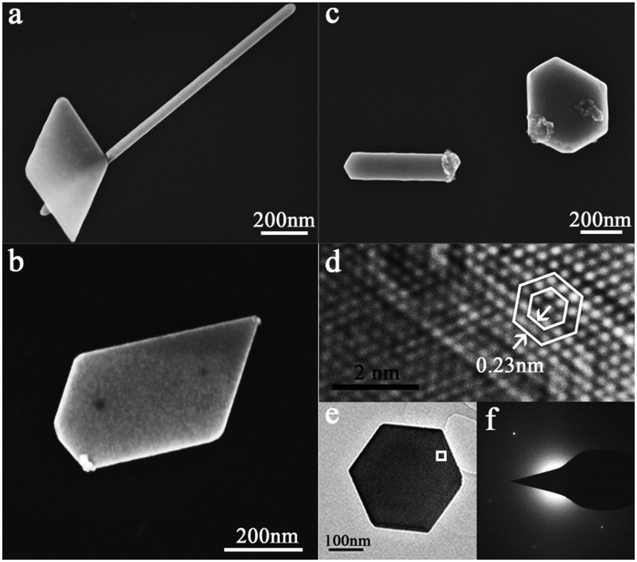 | ||
| Fig. 3 Zn nanoplates grown on the silicone oil surface (f = 0.01 nm s−1, d = 8.0 nm). (a–c) are SEM images of quadrangular, pentagonal and hexagonal Zn nanoplates, respectively. (d) is the high-resolution TEM image of the rectangular area of the hexagonal Zn nanoplate in (e). The lattice spacing of planes is marked in (d). (f) is the corresponding SAED pattern of (d). | ||
In order to investigate the microstructures of the Zn nanoplates, the TEM measurement of a hexagonal Zn nanoplate was carried out and the results are shown in Fig. 3d–f, from which we obtain that the lattice spacing of the atomic planes is 0.23 nm, corresponding to the (010) plane lattice parameter of the Zn crystal, i.e., the hexagonal Zn nanoplate is perpendicular to the [001] direction.
Besides, EDS measurement was performed to confirm the composition of the hexagonal Zn nanoplate, as shown in Fig. 4, indicating that the hexagonal nanoplate is composed of Zn. The Si and C signals are from the silicon wafer and the residual silicone oil.
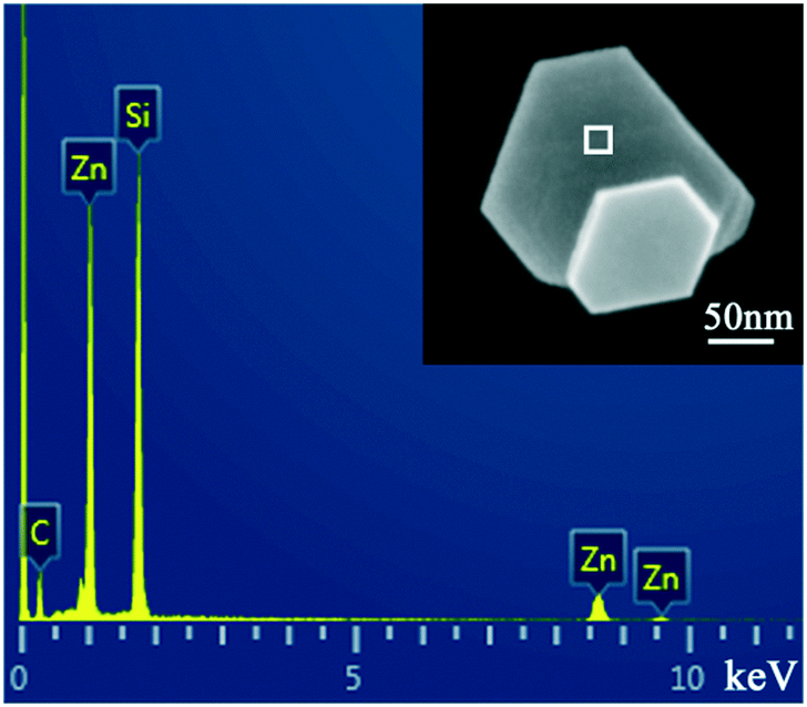 | ||
| Fig. 4 EDS spectrum of the white rectangular area of the hexagonal Zn nanoplate shown in the inset. | ||
For the sake of figuring out the tendency of the one- or two-dimensional growth, we plotted the aspect ratio distribution histogram of 142 Zn crystals prepared with f = 0.01 nm s−1, as shown in Fig. 5a. It is remarkable that the largest aspect ratio of the Zn crystals in our experiment may approach 159. The distribution shown in Fig. 5a may be well fitted by the lognormal distribution with the average aspect ratio of 12 and the most probable aspect ratio of around 5.
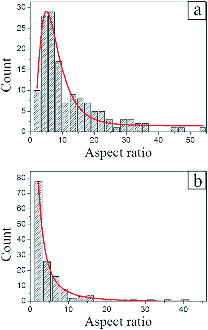 | ||
| Fig. 5 (a) and (b) show the aspect ratio distribution histograms of the Zn crystals prepared with deposition rates of 0.01 and 0.10 nm s−1, respectively (d = 8.0 nm). The solid curves are the lognormal and logistic distribution fitting of the experimental data, respectively. | ||
On the other hand, for f = 0.10 nm s−1, the one- and two-dimensional Zn crystals can still be found simultaneously on the silicone oil surface, however, as shown in Fig. 5b, their aspect ratio distribution is quite different from that shown in Fig. 5a. In this case, the largest value of the aspect ratios is 52, the average aspect ratio is 5, and more than half of the statistical data distribute in the range from 1 to 3.25, as shown in Fig. 5b. This result shows that a lower deposition rate is more beneficial to the growth of the one-dimensional crystals.
The aspect ratio distributions in Fig. 5 are the quantitative experimental evidence for the existence of the preferential growth directions. Since Zn crystals exhibit an hcp crystal structure and possess preferential growth directions, i.e., the [001] and [010] directions, the average aspect ratio should be closely related to the ratio between their growth priorities, namely δ. In other words, the value of δ should be approximately equal to the average aspect ratio. If this analysis is correct, according to the results shown in Fig. 5, we then estimate δ ≈ 100–101, i.e., the growth priorities of the preferential growth directions are not quite prominent and they may be sensitive to the experimental conditions (for instance, the deposition rate).
Therefore, the reasons above result in the competitive growth among different preferential growth directions of the Zn crystals on the silicone oil surface, which gives the explanation for the formation of the various crystal morphologies.
The growth mechanism of the one- and two-dimensional Zn crystals on the silicone oil surface is proposed as follows: (i) precursor Zn atoms nucleate randomly on the isotropic and quasi-free sustained liquid substrate, forming seed crystals; (ii) the seed crystals diffuse randomly and all the surrounding atoms in the effective diffusion area 〈Δr2〉 irreversibly aggregate to the seed crystals; (iii) the aggregated atoms may diffuse along the seed crystal surface until the lowest surface energies are reached, i.e., the morphologies of the Zn crystals are determined by the competitive growth among the preferential growth directions which may have different growth priorities.
The formation of the one-dimensional Zn crystals can be attributed to the different growth priorities of the lateral faces of the seed crystals. Obviously, a large difference among the priorities in different growth directions more easily leads to the one-dimensional growth of the Zn crystals. Since the anisotropic crystal structure results in an obvious tendency towards one-dimensional growth along the longer c-axis,33,34 the [001] direction of the Zn crystal may be considered as a growth direction with a high priority. Therefore, Zn crystal nanorods with a [001] growth direction may easily form on the isotropic and quasi-free sustained liquid surfaces. However, since the difference among the priorities is not very large and the ratio δ is a finite value, the preparation of one-dimensional Zn crystals with a very large aspect ratio is not easy experimentally and sometimes Zn nanorods and various Zn nanoplates may grow on the silicone oil surface simultaneously, as shown in Fig. 1b and 3.
In the case of the growth of the Zn nanoplate with its [001] direction upward, as shown in Fig. 3, it may be suggested that the lateral faces of the seed crystal possess a similar growth priority owing to the axisymmetric characteristics of the hcp crystal structure. As a result, it may weaken the one-dimensional growth. Eventually, it leads to the formation of polygonal plate-shaped structures with small aspect ratios corresponding to the left-hand members in Fig. 5.
The new aggregation mechanism above illustrates that one- and two-dimensional metallic nanocrystals may be fabricated on liquid surfaces simultaneously. However, the two-stage growth model26 shows that some metallic (silver,26 gold,35 aluminum,36 iron,37etc.) compact clusters and ramified aggregates with amorphous or polycrystalline microstructures can also be prepared on liquid surfaces. The discrepancy between them is obvious.
In fact, during deposition, after the metallic atoms reach the liquid substrate, they diffuse and aggregate. The nucleation process and the microstructures of the nucleus depend not only on the characteristics of the metallic atoms, but also on the interaction between the metallic atoms and the liquid molecules. Previous studies showed that, unlike Zn atoms, some metallic atoms, such as silver, gold, aluminum, iron, etc., aggregate on the liquid substrates and they prefer to form amorphous or polycrystalline clusters and ramified aggregates rather than crystals. Besides, the metallic crystals composed from these atoms possess relatively symmetrical crystal structures, i.e., face centered cubic (fcc) or body centered cubic (bcc) structures, in which the ratio δ of the growth priorities for the [001] and [010] directions is δ = 1. In other words, the fcc and bcc microstructures are disadvantages for the one-dimensional crystal growth relatively. Therefore, suitable metals, liquids and experimental conditions should be carefully selected for different purposes.
In addition to the one- and two-dimensional Zn crystals, Zn mounds also form on the silicone oil surface, as shown in Fig. 6. The Zn mounds are built from terraces scattering slightly around the shape of an equal-sided hexagon. From Fig. 6, we can obtain that the mean perimeters of the top terrace and the base terrace are 〈L〉 = 307 nm and 〈Λ〉 = 462 nm, respectively. The ratio of the two averages is 〈L〉/〈Λ〉 = 0.66. The most probable value of L, namely Lmax, is Lmax = 0.77〈Λ〉. From the inset of Fig. 6, steps with an average height of 16 nm can be measured exactly.
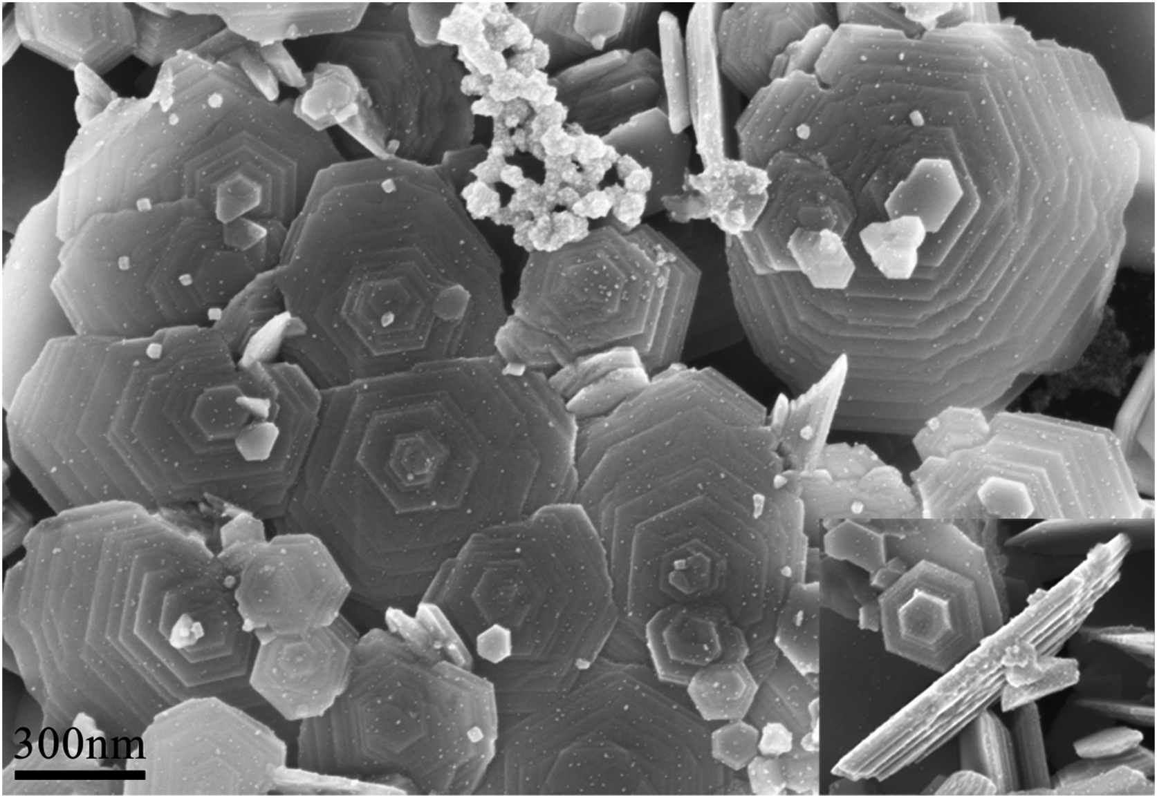 | ||
| Fig. 6 SEM image of Zn mounds grown on the silicone oil surface (f = 0.10 nm s−1, d = 8.0 nm). The inset displays the lateral morphology of a Zn mound under the same scale bar as the main figure. | ||
In terms of the formation of the Zn mounds, the step-edge barriers based on the hexagonal Zn nanoplates may play a crucial role. It has been shown that, compared to the diffusion barrier ED on an atomically flat terrace, an additional energy barrier ΔES should be overcome for an adatom to descend across a step edge on metal surfaces.18 This step-edge barrier has a decisive influence on the morphology of multilayer films by controlling the rate of interlayer mass transport.19,20 When the step-edge barriers are infinite, the coverages of the exposed layers follow a Poisson distribution and therefore the mounds possess a characteristic pointed shape.38 In the case of finite but large step-edge barriers, the pointed tip is replaced by a flat top terrace although the overall shape remains similar.39 In other words, the strength of the step-edge barrier determines the typical size of the top terrace.
Under the conditions of strong step-edge barriers, the mean size of the top terrace 〈L〉 and the most probable value Lmax are respectively given by  and Lmax/Λ = (k + 2)−1/(k+2)Γ[(k + 4)/(k + 2)]−1/2, where the size of the base terrace Λ is fixed for simplicity.19 It is obvious that this theory gives 〈L〉/Λ = 0.69 and Lmax/Λ = 0.80 for k = 5. Then, k = 5 can be translated into the critical cluster size i* on the base terrace being i* = 1, i.e., nucleation occurs instantaneously as soon as two adatoms are simultaneously present on the base terrace. Therefore, our results measured from Fig. 6, i.e., 〈L〉/〈Λ〉 = 0.66 and Lmax/〈Λ〉 = 0.77, are in good agreement with these theoretical predictions.
In view of this, the hexagonal Zn nanoplates in our experiment indeed possess large step-edge barriers contributing to the second-layer nucleation and the final formation of the Zn mounds. However, further experimental and theoretical investigations are still required for the specific step-edge barriers of the Zn mounds.
Interestingly, the average step height of the mounds with a value of 16 nm is much higher than that in the situation of epitaxial growth, where the step height is in the order of monolayers. Therefore, the preferential growth direction which is perpendicular to the hexagonal Zn nanoplate, i.e., the [001] direction of the Zn crystal, may provide an extra driving force to assist the growth in addition to the effect of the large step-edge barriers. All in all, the formation of the Zn mounds may be considered as the result of competitive growth in three-dimensional directions.
Conclusions
In summary, we have demonstrated a convenient and novel method to fabricate one-, two- and three-dimensional Zn crystals on a liquid surface at room temperature. The growth tendency of the one- and two-dimensional Zn crystals, which may be tunable by the deposition rate, can be attributed mainly to the preferential growth characteristics of the crystals. The Zn mounds with nanoscale steps may form on the liquid surface due to the large step-edge barriers and the upward preferential growth characteristics of the Zn crystals. A new aggregation mechanism involving competitive growth among the preferential growth directions is proposed and all the experimental phenomena can be explained successfully.The successful preparation of the one-dimensional Zn crystals and the Zn mounds with nanoscale steps on the silicone oil surface gives experimental evidence of the preferential growth characteristics of Zn crystals. On the other hand, the simultaneous presence of the one-, two- and three-dimensional Zn crystals on the silicone oil surface suggests that the growth priorities of the preferential growth directions are not quite prominent. According to the aspect ratio distributions and their average values, the ratio δ of the priorities in [001] and [010] directions may range in the order of magnitude from 100 to 101 and it may be tunable by the deposition rate.
At the moment, although several reports have mentioned the crystal preferential growth directions,11,31–34 there has been no specific result about the priority of various preferential growth directions yet. The effect of liquid substrates and the aggregation mechanism suggested above may provide a promising approach to figure out the exact priority of the different preferential growth directions by measuring statistical distributions of the growth directions of the crystals on various liquid surfaces.
Conflicts of interest
There are no conflicts of interest to declare.Acknowledgements
We thank Dr. Quanlin Ye, Tianliang Hao and Baoxing Li for technical assistance and useful discussions. The research was funded by the National Natural Science Foundation of China (Grant No. 11374082).References
- Y. Xia, P. Yang, Y. Sun, Y. Wu, B. Mayers, B. Gates, Y. Yin, F. Kim and H. Yan, Adv. Mater., 2003, 15, 353–389 CrossRef CAS.
- C. M. Lieber and Z. L. Wang, MRS Bull., 2007, 32, 99–108 CrossRef CAS.
- M. Li, R. B. Bhiladvala, T. J. Morrow, J. A. Sioss, K.-K. Lew, J. M. Redwing, C. D. Keating and T. S. Mayer, Nat. Nanotechnol., 2008, 3, 88–92 CrossRef CAS PubMed.
- A. Singh, T. P. Sai and A. Ghosh, Appl. Phys. Lett., 2008, 93, 102107 CrossRef.
- G. Li, B. Wang, Y. Liu, T. Tan, X. Song and H. Yan, Appl. Surf. Sci., 2008, 255, 3112–3116 CrossRef CAS.
- E. Deiss, F. Holzer and O. Haas, Electrochim. Acta, 2002, 47, 3995–4010 CrossRef CAS.
- L. Veleva, E. Meraz and M. Acosta, Mater. Corros., 2007, 58, 348–352 CrossRef CAS.
- J.-G. Wang, M.-L. Tian, N. Kumar and T. E. Mallouk, Nano Lett., 2005, 5, 1247–1253 CrossRef CAS PubMed.
- D. Pradhan, S. Sindhwani and K. T. Leung, J. Phys. Chem. C, 2009, 113, 15788–15791 CAS.
- M. Tian, N. Kumar, S. Xu, J. Wang, J. S. Kurtz and M. H. W. Chan, Phys. Rev. Lett., 2005, 95, 076802 CrossRef PubMed.
- M. Kast, P. Schroeder, Y. J. Hyun and P. Pongratz, Nano Lett., 2007, 7, 2540–2544 CrossRef CAS PubMed.
- S. Kar, T. Ghoshal and S. Chaudhuri, Chem. Phys. Lett., 2006, 419, 174–178 CrossRef CAS.
- Y. Yan, P. Liu, M. J. Romero and M. M. Al-Jassim, J. Appl. Phys., 2003, 93, 4807–4809 CrossRef CAS.
- C. Lu, Y. Cheng, Q. Pan, X. Tao, B. Yang and G. Ye, Sci. Rep., 2016, 6, 19870 CrossRef CAS PubMed.
- P. X. Gao, C. S. Lao, Y. Ding and Z. L. Wang, Adv. Funct. Mater., 2006, 16, 53–62 CrossRef CAS.
- H. Ma, C. Li, Y. Su and J. Chen, J. Mater. Chem., 2007, 17, 684–691 RSC.
- G. Jiangfeng, Y. Shaoguang, H. Hongbo, Z. Xiaoning and Y. Zhong-Zhen, Nanotechnology, 2007, 18, 235606 CrossRef.
- G. Ehrlich and F. G. Hudda, J. Chem. Phys., 1966, 44, 1039–1049 CrossRef CAS.
- J. Krug, P. Politi and T. Michely, Phys. Rev. B: Condens. Matter Mater. Phys., 2000, 61, 14037–14046 CrossRef CAS.
- Z. Zhang and M. G. Lagally, Phys. Rev. Lett., 1994, 72, 693–696 CrossRef CAS PubMed.
- R. S. Devan, J.-H. Lin, Y.-J. Huang, C.-C. Yang, S. Y. Wu, Y. Liou and Y.-R. Ma, Nanoscale, 2011, 3, 4339–4345 RSC.
- P. E. Acuña-Avila, R. López, E. Vigueras-Santiago, S. Hernández-López, M. Camacho-López, C. Ornelas-Gutierrez and W. Antunez, AIP Adv., 2015, 5, 067109 CrossRef.
- Z. W. Pan, Z. R. Dai and Z. L. Wang, Science, 2001, 291, 1947 CrossRef CAS PubMed.
- R. S. Wagner and W. C. Ellis, Appl. Phys. Lett., 1964, 4, 89–90 CrossRef CAS.
- T. J. Trentler, K. M. Hickman, S. C. Goel, A. M. Viano, P. C. Gibbons and W. E. Buhro, Science, 1995, 270, 1791–1794 CAS.
- G. X. Ye, T. Michely, V. Weidenhof, I. Friedrich and M. Wuttig, Phys. Rev. Lett., 1998, 81, 622–625 CrossRef CAS.
- M.-B. Luo, G.-X. Ye, A. G. Xia, J.-S. Jin, B. Yang and J.-M. Xu, Phys. Rev. B: Condens. Matter Mater. Phys., 1999, 59, 3218–3223 CrossRef CAS.
- A. Einstein, Ann. Chim. Phys., 1905, 322, 549–560 CrossRef.
- A. Einstein, Ann. Chim. Phys., 1906, 324, 371–381 CrossRef.
- I. N. Levine, Physical chemistry, McGraw-Hill, New York, 3rd edn, 1988 Search PubMed.
- W. Qun, C. Gang and Z. Nan, Nanotechnology, 2009, 20, 085602 CrossRef PubMed.
- S. Cho and K.-H. Lee, J. Mater. Chem., 2010, 20, 6982–6989 RSC.
- B. Mayers, B. Gates, Y. Yin and Y. Xia, Adv. Mater., 2001, 13, 1380–1384 CrossRef CAS.
- P. Mohanty, T. Kang, B. Kim and J. Park, J. Phys. Chem. B, 2006, 110, 791–795 CrossRef CAS PubMed.
- G.-X. Ye, A. G. Xia, G.-L. Gao, Y.-F. Lao and X.-M. Tao, Phys. Rev. B: Condens. Matter Mater. Phys., 2001, 63, 125405 CrossRef.
- Q.-F. Pan, Y. Cheng, X.-M. Tao, B. Yang, B.-X. Li and G.-X. Ye, J. Nanopart. Res., 2015, 17, 161 CrossRef.
- N. Lü, Q.-F. Pan, Y. Cheng, B. Yang and G.-X. Ye, Chin. Phys. B, 2013, 22, 116103 CrossRef.
- P. I. Cohen, G. S. Petrich, P. R. Pukite, G. J. Whaley and A. S. Arrott, Surf. Sci., 1989, 216, 222–248 CrossRef CAS.
- P. Politi, J. Phys. I, 1997, 7, 797–806 CrossRef.
| This journal is © The Royal Society of Chemistry 2018 |