
 Open Access Article
 This Open Access Article is licensed under a Creative Commons Attribution-Non Commercial 3.0 Unported Licence
Surface enhanced Raman scattering (SERS) in the visible range on scalable aluminum-coated platforms†
Manuel
Gómez
ab,
Shima
Kadkhodazadeh
 c and
Massimo
Lazzari
*ab
c and
Massimo
Lazzari
*ab
aDepartamento de Química Física, Facultade de Química, Universidade de Santiago de Compostela, 15782 Santiago de Compostela, Spain. E-mail: massimo.lazzari@usc.es
bCentro Singular de Investigación en Química Biolóxica e Materiais Moleculares (CIQUS), Universidade de Santiago de Compostela, 15782 Santiago de Compostela, Spain
cDanchip/Center for Electron Nanoscopy (CEN), Technical University of Denmark, Kgs. Lyngby 2800, Denmark
First published on 4th September 2018
Abstract
We demonstrate the potential of combining plasmonic Bragg grating structures, with the scattering effect of a rough Al layer to tune SERS enhancement in the visible region. Novel Al-based substrates with good analytical reproducibility and enhancement factors in the range of 107–109 are produced by a scalable procedure which meets the development of producing sustainable SERS platforms.
Since the first observation of unusually intense Raman signals from an aqueous solution of pyridine in contact with roughened silver electrodes,1 the phenomenon known as surface enhanced Raman scattering (SERS) has been the subject of more than 15
![[thin space (1/6-em)]](https://www.rsc.org/images/entities/char_2009.gif) 000 studies in over 40 years of research, with the first peak of interest in the late 90s.2 It is generally understood that the dominant contribution to SERS processes arises from the interaction of the Raman transition moment of the adsorbed molecules with the light-induced electromagnetic fields (localized surface plasmon resonance, LSPR) on the metal surface.3 In the last few years there has been a renewed interest in both basic research and application of SERS, owing to improvements in the Raman spectroscopy technology and development of more accurate and flexible techniques for fabrication and manipulation of nanomaterials.4 Previously, Ag and Au nanoparticles with tailored size, shape and coupling distance were the popular choice in designing active SERS substrates.5 More recent advances in this field include coating plasmonic nanostructures6 (or other forms of hybrid nanomaterials4), development of 3D substrates by assembling nanoparticles7 through top-down approaches8 and taking advantage of metal-coated natural mesostructured surfaces.9 In particular, the fabrication of complex nanostructure metallic supports with void architectures (fabricated by self-assembling, templating or lithographic-based technologies) is opening new fascinating routes to expand the limits of SERS’ reproducibility and commercial applications.10 As an example, the control of periodicity in submicrometer highly ordered structures allows the tuning of the optical response of the SERS substrates, originating from the narrow Bragg surface plasmon polariton resonances, to the specific wavelength of the Raman excitation laser.8a,b,11 This versatility enables the use of alternative plasmonic materials beyond those classically based on gold and silver. To some extent, it also enables the creation of regions with extremely high field confinement, so-called hot spots, via the control of the substrate geometry, rather than the nature of the metal or the dielectric constant of the embedding medium.12
000 studies in over 40 years of research, with the first peak of interest in the late 90s.2 It is generally understood that the dominant contribution to SERS processes arises from the interaction of the Raman transition moment of the adsorbed molecules with the light-induced electromagnetic fields (localized surface plasmon resonance, LSPR) on the metal surface.3 In the last few years there has been a renewed interest in both basic research and application of SERS, owing to improvements in the Raman spectroscopy technology and development of more accurate and flexible techniques for fabrication and manipulation of nanomaterials.4 Previously, Ag and Au nanoparticles with tailored size, shape and coupling distance were the popular choice in designing active SERS substrates.5 More recent advances in this field include coating plasmonic nanostructures6 (or other forms of hybrid nanomaterials4), development of 3D substrates by assembling nanoparticles7 through top-down approaches8 and taking advantage of metal-coated natural mesostructured surfaces.9 In particular, the fabrication of complex nanostructure metallic supports with void architectures (fabricated by self-assembling, templating or lithographic-based technologies) is opening new fascinating routes to expand the limits of SERS’ reproducibility and commercial applications.10 As an example, the control of periodicity in submicrometer highly ordered structures allows the tuning of the optical response of the SERS substrates, originating from the narrow Bragg surface plasmon polariton resonances, to the specific wavelength of the Raman excitation laser.8a,b,11 This versatility enables the use of alternative plasmonic materials beyond those classically based on gold and silver. To some extent, it also enables the creation of regions with extremely high field confinement, so-called hot spots, via the control of the substrate geometry, rather than the nature of the metal or the dielectric constant of the embedding medium.12
The interest in Al plasmonics is relatively recent and mainly relies on its low cost and ease of processing by a variety of methods.13 The original studies on Al nanospheres and nanodisks14 demonstrated their potential at least in the UV region. Halas et al. showed that strict control of the size and purity of the Al nanodisks (50–200 nm) drives the plasmon resonance in the approximate range of 2.0–5.0 eV (λ = 620–250 nm).15 In more recent studies, Halas and co-workers also reported the fabrication of a full color tunable plasmonic device based on a 2D period array of rectangularly shaped Al nanostructures,16 whereas Lay et al. established lithographically fabricated Al nanodot arrays as promising SERS-based security labels in the visible region.17
Experimental and theoretical studies have pointed out that the plasmon resonance in Al nanoparticle arrays can also be tuned by varying the particle height and interparticle distance, and the dipolar LSPR peak obtained at 5.3 eV (234 nm) is among the shortest resonance wavelengths ever observed in patterned Al.18 Other works have demonstrated the potential of large scale Al nanovoid-type substrates and other Al structures for deep UV-SERS detection of organics and biomacromolecules.10,19 Interestingly, in a work studying the effect of thermal annealing of Al films, where rough, discontinuous surfaces were used as SERS substrates, hot spots in the NIR region were reported.20 Such surface discontinuities thus provide an additional dial for fine-tuning the plasmon resonance energy in a range spanning from NIR to UV.
Herein, we demonstrate the potential of combining precise Bragg resonance diffraction with LSPRs originating from discontinuities in nanostructured metal films to extend SERS enhancement over a wide frequency range. Our investigation explores the application of Al as an alternative plasmonic material in the visible region, using elastomeric micrometer periodic structures easily produced by nanoimprint lithography (NIL) and coated with an Al layer of controlled roughness. With respect to gold-coated pyramidal features produced by controlled etching onto silicon-wafer,21 this procedure is easily scalable through simpler and cost-effective roll-to-roll processes, and allows robust plastic substrates which show long term stability and constant performance to be obtained.
Squared arrays of elastomeric positive and inverted pyramids, as shown in Fig. 1 and in the ESI† (Fig. S1), were fabricated by single- or multiple-step molding and replication UV-NIL processes. The master mold was selected among those commercially available with large-scale periodicity that could satisfy the requirement of leading to Bragg diffraction in the NIR wavelengths. The surface of the replica on the UV-curable material (either an ORMOCER or a tetraurethane methacrylate perfluoropolyether22) is rather smooth and the fine tuning of the optical properties of the structure is achieved through the deposition of a metal coating. Al deposition by thermal evaporation with an evaporation rate of 50 Å s−1 produced substrates with RMS roughness of 27.9 nm both in the pit sidewalls and in the flat surfaces in between. The randomly oriented Al nanocrystals with regular shapes and dimensions (10–50 nm), and an average particle height of 5.4 nm, can be seen clearly in the higher magnification SEM image in Fig. 1 and in the TEM images in Fig. S3 (ESI†). Faster or slower evaporation rates produced crystals either too large or too small resulting in surface morphologies, i.e. SERS substrates, unable of sustaining plasmonic resonances in the frequency range of interest.8b,11 An Al thickness of at least 150 nm was selected due to two main reasons: first to ensure the film's opacity to laser light and to avoid fluorescence and Raman signals from the polymeric matrix. Second, to have sufficient thickness of the metal, acting as a heat sink and increasing the locally accumulated heat by the laser beam during the measurement.
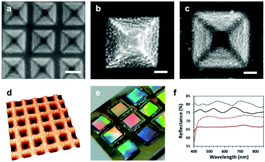 | ||
| Fig. 1 SEM micrographs of inverted (a and c) and positive (b) pyramid substrates. Scale bars are 1 μm for the array and 200 nm for single pyramid images. Non-contact AFM 3D reconstruction of Al-coated inverted pyramid arrays (d). Photograph of 5 × 5 mm Al-coated substrates (e). Reflection spectra of Al-coated inverted and positive pyramid substrates (solid and dashed curve, respectively; magnification in Fig. S2, ESI†), and corresponding uncoated substrates (red curves) (f). | ||
The combination of surface roughness and micrometer arrays is expected to affect the optical properties of the substrates. Reflection spectra of Al-coated surfaces are compared with those of the corresponding bare substrates in Fig. 1f. The transformation from a purely dielectric to a metallic periodically-modulated surface allows the propagation of surface plasmon polaritons, and contributes to the appearance of a series of well-defined dips superimposed on the constant reflectivity profile expected from flat Al films.20 Although only the collection of dispersion curves would unambiguously prove the nature of the plasmons,23 a simpler speculation may alternatively support their origin. Within this concise account, the observation of reflectance dips at 590 and 780 nm, closely matching those observed for inverted pyramids with a 300 nm gold coating,21 may also indicate in our system their nature of Bragg resonances coupled through the periodic lattice. We experimentally relate the other reflectance dips at lower wavelengths, not visible in gold-coated substrates,9 to the LSPRs of the grainy Al surface, as they are also present in the high spatial resolution electron energy-loss spectroscopy (EELS) measurements discussed later on.
The SERS performance of the substrates in the wavelength range of interest was established using rhodamine 6G (R6G) and coumarin 440 as target analytes, and 514 and 785 nm excitations (spectra are shown in Fig. 2, and further examples in Fig. S4–S9, ESI†). A small amount of dilute ethanol solution (around 0.025 μL) was dropped onto the substrate and formed a dried sample area of around 0.2 mm2. As the laser spot area is around 60 μm2, the measurements were carried out in the central part of the droplet to avoid taking measurements from any aggregated regions at the edges. Spectra of both analytes from solutions in the concentration range of 1 × 10⁻⁶–1 × 10⁻¹⁵ M showed their distinctive peaks with relative changes in the intensity of some peaks, usually attributed to changes in orientation and enhancement.19 The surface enhancement factor, EF, was calculated following the schematization by Le Ru et al.24 As presented in Table S1 (ESI†), in the case of inverted pyramid arrays EF values that exceed 107 are obtained upon illumination of the substrates at 785 nm, and produce higher enhancements up to >109 (inverse pyramid arrays, for R6G) out of the Bragg resonance, i.e. when illuminated by the 514 nm laser. On average, positive pyramids produce lower corresponding EFs, but nevertheless in the range 106–108. These EFs are higher than values observed for smooth gold-coated pyramidal features,9,21 and consistent with those reported for other demanding gold or silver-coated 3D substrates.8b,c,11
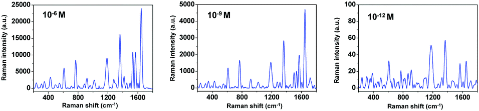 | ||
| Fig. 2 Raman spectra of R6G from solutions with different concentrations at 514 nm excitation wavelength on an inverted pyramid SERS device (10 s exposure time, power 0.09 mW). | ||
Finite difference time domain (FDTD) simulation of the electric field intensity distribution offers a first insight into the near-field phenomena responsible for the observed enhanced emission. The simulated spatial distribution of the electric field intensity corresponding to the vertical cross-sections of smooth Al-coated inverted pyramids illuminated with a plane wave at 514 nm is shown in Fig. 3. The enhancement of the scattered electrical field has a very similar spatial distribution in response to both the 514 and 785 nm wavelengths, although with different relative intensity, and is especially visible in the lower part of the smooth sidewalls of the inverted pyramids. The higher intensity of the enhancement calculated at 785 nm excitation wavelength supports the nature of the corresponding surface plasmon polariton mode excited through the 2D lattice. On the contrary, the lower values of the electric field intensity obtained for 514 nm incident light possibly indicates that there are no plasmon resonances directly due to the 2D grating at this wavelength, as also discussed earlier in relation to the reflectance spectra. Hot spots at the gaps and edges of the surface due to the roughness of the Al film are expected here to play an important role.8b,11 However, a precise simulation of LSPR modes onto a discontinuous surface is not trivial, due to the random distribution of Al grains, and was not considered further in this introductory exploration.
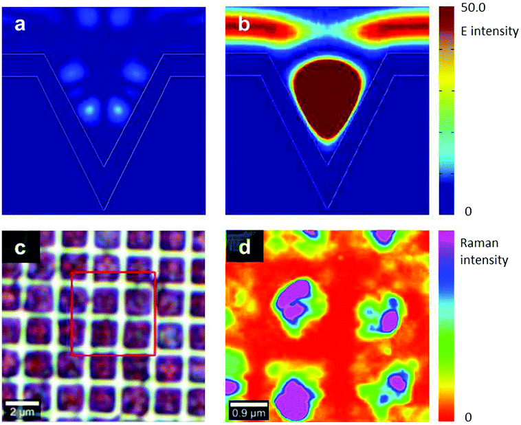 | ||
| Fig. 3 FDTD simulated electric field intensity distribution in the ideal Al-coated inverted pyramid arrays excited with a plane wave at 514 nm (a) and 785 nm (b), and confocal Raman imaging map of R6G from 1 × 10⁻⁶ M solution at 514 nm excitation wavelength on an inverted pyramid SERS device (d) obtained from the red square area of the photograph (c). | ||
In the case of our substrates, confocal Raman imaging can obtain the first experimental indication of the approximate SERS activity of R6G as shown in Fig. 3d which reveals intense Raman signals in the sidewalls of the pyramids, with a good reproducibility at different locations for all of the area corresponding to the extent of the sample solution droplet. Conversely, a negligible Raman response is detected in the flat areas between the pyramids, even though the analyte is also present there. Additionally, we have studied the spatial distribution of the surface plasmons supported by our substrates using EELS.
EELS carried out on a (scanning) transmission electron microscope ((S)TEM) allows the mapping of surface plasmons with nanometer resolution,25 since unlike optical measurements, EELS measurements are not limited by the diffraction limit of light. Our EELS measurements were acquired using an aberration corrected FEI Titan (S)TEM instrument fitted with a monochromator, and operated at 120 kV accelerating voltage, giving spatial and energy resolutions of approximately 0.5 nm and 0.15 eV, respectively. The Al free-standing layer was examined after removing the polymer from an inverted pyramids substrate by acetone dissolution. A high-angle annular dark-field (HAADF) STEM image of the inverted Al pyramids is presented in Fig. 4a. The core-loss EELS signal from the examined pyramids confirms that the sample contains only a very thin oxide layer (as visible in Fig. S10, ESI†), which is expected to significantly affect neither the magnitude of the surface enhancement nor the plasmonic resonance frequency.19 EEL spectra from an approximately 2 × 2 μm area across the pyramid in Fig. 4b were acquired using a step size of 15 nm. EEL spectra showing surface plasmon resonances at 1.35 eV and 2.5 eV, matching approximately the laser excitation wavelengths at 785 nm and 514 nm giving strong SERS signals, are presented in Fig. 4c and e, respectively. The intensity maps of the surface plasmon resonances at 1.35 eV and 2.5 eV, produced by integrating the EEL signal over a 0.3 eV energy window, are presented in Fig. 4d and f, respectively. Strikingly, the intensity map for the excitation at 1.35 eV reveals some localization along the diagonals of the pyramid (Fig. 4d). In contrast, the EELS intensity map of the 2.5 eV surface plasmon mode corresponds more closely to the surface roughness of the Al film (Fig. 4f). In both cases, little signal intensity is detected in the flat regions between the pyramids.
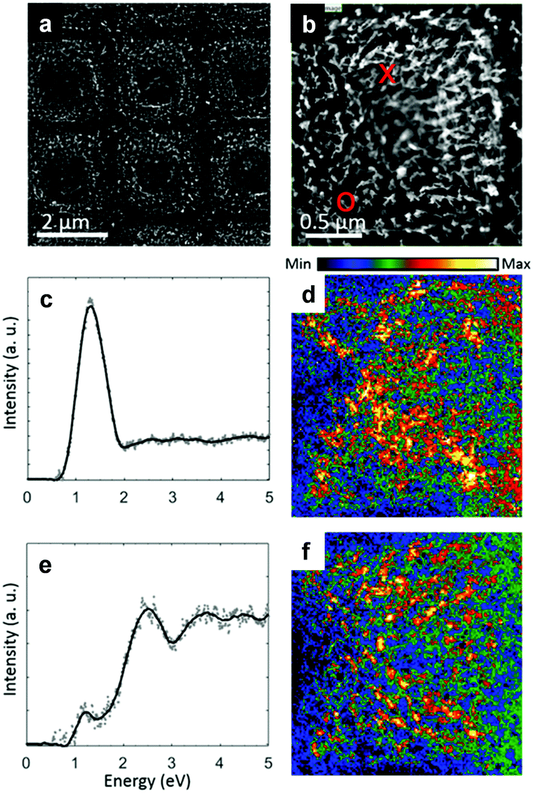 | ||
| Fig. 4 HAADF STEM image of the Al layer with inverted pyramids (a). HAADF STEM image of a single pyramid, where the EELS measurements were recorded from (b). EEL spectra showing intense surface plasmon signals at 1.35 eV (c) and 2.5 eV (e), as collected from the points with red X and O marks, respectively, in image (b). Corresponding intensity maps with integrated intensity in the energy range of 1.2–1.5 eV (d) and 2.35–2.65 eV (f), respectively. | ||
On one side, it is clear that the roughness of Al in the inter-pyramid flat region is not enough to sustain LSPR, but when the rough surface inside the pyramidal pits is illuminated by the radiation within the range 1.2–1.6 eV (an energy corresponding approximately to the 785 nm wavelength) the surface plasmon polaritons launched through the grating periodicity excite resonances at the edges of the Al grains. In a similar way, one may suppose that the loss of energy in the 2.35–2.65 eV range, experimentally verified by the Raman measurements at 514 nm excitation, is due to a hybrid plasmon resonance resulting from the coupling of the Bragg modes and the strong scattering effect of the surface roughness. A similar effect has been observed on rough silver-coated substrates.8b Additionally, the common features of high-field confinements around the diagonals may be justified because of the well-known phenomena of light trapping within this geometry,26 in which higher intensities of both the Bragg and the hybrid resonances are supposed to be obtained when the light wave reaches the edges of the sidewalls of the pyramids. Such enhancement heterogeneity is intrinsic in SERS substrates,2 and also in this case it is an accepted notion that the local effects are mediated onto the large area of the measurements.
In conclusion, we showed that the coupling of Bragg surface plasmon polariton resonances originated by submicrometer 3D structures with the characteristic scattering effect due to the nanometer-sized surface roughness of the Al coating may produce SERS substrates active in the visible range. Their cost-effective fabrication using the soft lithography method combined with controlled Al deposition over millimeter-sized dimensions meets the development trend of producing sustainable SERS platforms. Finally, also by comparison with available gold-coated substrates with pyramidal features, the better values of EF, proved long term stability and the limited requirements of analyte preparation make these SERS substrates suitable for demanding analytical purposes, e.g., in forensic science and cultural heritage studies.27
The European Union (Project NANORESTART: H2020-NMP-21-2014/646063 and European Regional Development Fund) and the Xunta de Galicia (Centro singular de investigación de Galicia accreditation 2016–2019, ED431G/09) supported this work. The A. P. Møller and Chastine Mc-Kinney Møller Foundation are gratefully acknowledged for their contribution towards the establishment of the Centre for Electron Nanoscopy in the Technical University of Denmark.
Conflicts of interest
There are no conflicts to declare.Notes and references
- M. Fleischmann, P. J. Hendra and A. J. McQuillan, Chem. Phys. Lett., 1974, 26, 163 CrossRef.
- M. Moskovits, Phys. Chem. Chem. Phys., 2013, 15, 5301 RSC.
- (a) P. K. Aravind, A. Nitzan and H. Metiu, Surf. Sci., 1981, 110, 189 CrossRef; (b) M. Moskovits, Rev. Mod. Phys., 1985, 57, 783 CrossRef; (c) E. Prodan, C. Radloff, N. J. Halas and P. A. Nordlander, Science, 2003, 302, 419 CrossRef PubMed.
- J. F. Li, Y. F. Huang, Y. Ding, Z. L. Yang, S. B. Li, X. S. Zhou, F. R. Fan, W. Zhang, Z. Y. Zhou, D. Y. Wu, B. Ren, Z. L. Wang and Z. Q. Tian, Nature, 2010, 464, 392 CrossRef PubMed.
- (a) K. Kneipp, H. Kneipp and J. Kneipp, Acc. Chem. Res., 2006, 39, 443 CrossRef PubMed; (b) A. Gutés, C. Carraro and R. Maboudian, J. Am. Chem. Soc., 2010, 132, 1476 CrossRef PubMed; (c) J. Langer, S. M. Novikov and L. M. Liz-Marzan, Nanotechnology, 2015, 26, 322001 CrossRef PubMed; (d) W. Xie and S. Schlücker, Chem. Commun., 2018, 54, 2326 RSC.
- (a) S. Mubeen, S. Zhang, N. Kim, S. Lee, S. Krämer, H. Xu and M. Moskovits, Nano Lett., 2012, 12, 2088 CrossRef PubMed; (b) H. S. Fateixa, H. I. S. Nogueira and T. Trindade, Phys. Chem. Chem. Phys., 2015, 17, 21046 RSC.
- C. H. Lee, L. Tian and S. Singamaneni, ACS Appl. Mater. Interfaces, 2010, 2, 3429 CrossRef PubMed.
- (a) Z. Xu, H.-Y. Wu, S. U. Ali, J. Jiang, B. T. Cunningham and G. L. Liu, J. Nanophotonics, 2011, 5, 053526 CrossRef; (b) G. Macias, M. Alba, L. F. Marsal and A. Mihi, J. Mater. Chem. C, 2016, 4, 3970 RSC; (c) J. Jiang, Z. Xu, A. Ameen, F. Ding, G. Lin and G. L. Liu, Nanotechnology, 2016, 27, 385205 CrossRef PubMed.
- F. Shao, Z. Lu, C. Liu, H. Han, K. Chen, W. Li, Q. He, H. Peng and J. Chen, ACS Appl. Mater. Interfaces, 2014, 6, 6281 CrossRef PubMed.
- T. Ding, D. O. Sigle, L. O. Herrmann, D. Wolverson and J. J. Baumberg, ACS Appl. Mater. Interfaces, 2014, 6, 17358 CrossRef PubMed.
- T.-W. Chang, S. Seo, H. Jin, X. Wang and G. L. Liu, J. Phys. Chem. C, 2014, 118, 18693 CrossRef.
- M. Essone Mezeme and C. Brosseau, Opt. Express, 2012, 20, 17591 CrossRef PubMed.
- D. Gérard and S. K. Gray, J. Phys. D: Appl. Phys., 2015, 48, 180301 CrossRef.
- C. Langhammer, M. Schwind, B. Kasemo and I. Zoric, Nano Lett., 2008, 8, 1461 CrossRef PubMed.
- M. J. McClain, A. E. Schlather, E. Ringe, N. S. King, L. Liu, A. Manjavacas, M. W. Knight, I. Kumar, K. H. Whitmire, H. O. Everitt, P. Nordlander and N. J. Halas, Nano Lett., 2015, 15, 2751 CrossRef PubMed.
- M. L. Tseng, J. Yang, M. Semmlinger, C. Zhang, P. Nordlander and N. J. Halas, Nano Lett., 2017, 17, 6034 CrossRef PubMed.
- C. L. Lay, C. S. L. Koh, J. Wang, Y. H. Lee, R. Jiang, Y. Yang, Z. Yang, I. Y. Phang and X. Y. Ling, Nanoscale, 2018, 10, 575 RSC.
- C. C. Zhao, Y. Zhu, Y. Q. Su, Z. Y. Guan, A. Q. Chen, X. Ji, X. C. Gui, R. Xiang and Z. K. Tang, Adv. Opt. Mater., 2015, 3, 248 CrossRef.
- (a) D. O. Sigle, E. Perkins, J. J. Baumberg and S. Mahajan, J. Phys. Chem. Lett., 2013, 4, 1449 CrossRef PubMed; (b) A. Taguchi, N. Hayazawa, K. Furusawa, H. Ishitobi and S. Kawata, J. Raman Spectrosc., 2009, 40, 1324 CrossRef; (c) S. K. Jha, Z. Ahmed, M. Agio, Y. Ekinci and J. F. Löffler, J. Am. Chem. Soc., 2012, 134, 1966 CrossRef PubMed.
- K. B. Mogensen, M. Gühlke, J. Kneipp, S. Kadkhodazadeh, J. B. Wagner, M. Espina Palanco, H. Kneipp and K. Kneipp, Chem. Commun., 2014, 50, 3744 RSC.
- N. M. B. Perney, J. J. Baumberg, M. E. Zoorob, M. D. B. Charlton, S. Mahnkopf and C. M. Netti, Opt. Express, 2006, 14, 847 CrossRef PubMed.
- (a) M. Gómez and M. Lazzari, Microelectron. Eng., 2012, 97, 208 CrossRef; (b) M. Gómez and M. Lazzari, Mater. Today, 2014, 17, 358 CrossRef.
- As a matter of fact, a detailed study of the dispersion characteristics of these and other periodically-modulated substrates will be the subject of a full paper.
- E. C. Le Ru, E. Blackie, M. Meyer and P. G. Etchegoin, J. Phys. Chem. C, 2007, 111, 13794 CrossRef.
- (a) F. J. Garcia de Abajo, Rev. Mod. Phys., 2010, 82, 209 CrossRef; (b) S. Kadkhodazadeh, J. B. Wagner, V. Joseph, J. Kneipp, H. Kneipp and K. Kneipp, Plasmonics, 2013, 8, 763 CrossRef.
- A. Mavrokefalos, S. E. Han, S. Y. Yerci, M. S. Branham and G. Chen, Nano Lett., 2012, 12, 2792 CrossRef PubMed.
- M. Gómez, D. Reggio and M. Lazzari, J. Raman Spectrosc., in press Search PubMed.
Footnote |
| † Electronic supplementary information (ESI) available: Experimental details, a table and additional Fig. S1–S10. See DOI: 10.1039/c8cc04280b |
| This journal is © The Royal Society of Chemistry 2018 |