In situ synthesis of Bi nanoflakes on Ni foam for sodium-ion batteries†
Liubin
Wang
,
Chenchen
Wang
,
Fujun
Li
 *,
Fangyi
Cheng
 and
Jun
Chen

Key Laboratory of Advanced Energy Materials Chemistry (Ministry of Education), College of Chemistry, Nankai University & Collaborative Innovation Center of Chemical Science and Engineering, Tianjin 300071, P. R. China. E-mail: fujunli@nankai.edu.cn
First published on 21st November 2017
Abstract
We report a facile method to in situ synthesize Bi nanoflakes on Ni foam (Bi/Ni) via a replacement reaction, which can directly work as an anode for sodium-ion batteries (SIBs) without further treatment. The integrated nanoflake structure of the Bi/Ni effectively accommodates the dramatic volume changes of Bi during cycling, and favors both electron and Na+ transport through the electrode. This ensures high cycling performance and good rate capability. The sodiation/desodiation of Bi is revealed to be composed of two successive steps: Bi ↔ NaBi and NaBi ↔ Na3Bi. This facile strategy will encourage more investigations into the design and synthesis of integrated electrodes for high-performance SIBs.
The availability of scalable and high-performance anode materials is the key to promoting the development of sodium-ion batteries (SIBs).1,2 Attempts have been made ranging from carbon materials to metal oxides, metal sulfides, and alloys, etc.3–6 Unlike the Li+ counterpart, Na+ has a more positive redox potential and a larger radius, which rule out most of the candidates for Li storage. Among them, alloys have been recognized as one of the promising anodes for SIBs for multiple electron storage and hence large specific capacities.7–9 However, the dramatic volume change of alloys during sodiation and desodiation over 100% usually results in particle pulverization and cracking of electrodes, and therefore loss of electric contact and degradation of electrochemical performance.10,11 A rational design of the micro/nanostructures of alloys has been demonstrated to reduce such an effect on electrode performance,12,13 and is of significant importance to boost the performance of SIBs.
Nanostructured materials have been widely demonstrated to promote the electrochemical performance.14–16 They can efficiently reduce the strain caused by Na+ insertion/extraction into the electrode and thus maintain its integrity. As a promising anode candidate, Bi of various nanostructures has been created to improve its battery performance. Shao et al. developed a low-temperature hydrothermal method to prepare Bi nanotubes using aqueous hydrazine as the reductant.17 They showed improved kinetics and cycling stability for Mg storage. Bi nanorod bundles were obtained via a chemical dealloying process by Liu et al. for anodes of SIBs.18 Sottmann et al. revealed the crystallite size effect of Bi nanoparticles on the alloying with Na and then the cycling behavior.19 Supported by graphene, Bi nanoparticles exhibited two typical sodiation/desodiation plateaus with decaying capacities, as reported by Wang's group.20 Nano-networks of Bi generated during electrochemical processes effectively promoted its cycling stability.21 However, the integration of Bi with controllable nanostructures onto current collectors without binders and conductive agents and its contribution to reversible sodiation and desodiation have not ever been revealed.
Herein, we report a facile synthesis method to in situ produce Bi nanoflakes on Ni foam (Bi/Ni) via a replacement reaction, which are directly employed as an anode for SIBs without further treatment. The Bi nanoflakes are generated with a slow reduction of Bi3+ by Ni foam. The as-synthesized Bi/Ni features a three-dimensional (3D) structure with the Bi nanoflakes integrated on the Ni foam. Such a unique structure benefits the penetration of electrolyte, conduction of electrons, and tolerance towards the dramatic volume change of Bi during sodiation/desodiation. The Bi/Ni exhibits good cycling stability and rate capability. The facile method and high electrochemical performance of Bi/Ni will encourage more investigations into the design and synthesis of integrated electrodes for SIBs.
A facile process to produce the Bi/Ni anode is schematically shown in Scheme 1. When submerging Ni foam into an ethylene glycol solution of Bi3+, the color of the Ni foam slowly changes from silver white to dark grey, and simultaneously the solution changes to light green, as shown in Scheme 1a. These results indicate the formation of Bi metal and Ni2+ ions in the solution. The replacement reaction between Ni and Bi3+ is warranted by the lower redox potential of Ni2+/Ni than Bi3+/Bi (−0.246 vs. 0.308 V against normal hydrogen electrode, NHE),22–24 as depicted in Scheme 1b and c. The Ni foam serves not only as a reducing agent for the conversion of Bi3+ to Bi, but also as a substrate for the growth of Bi nanoflakes (Scheme 1b). The microstructures and thickness of Bi can be facilely controlled by the concentration of Bi3+, synthesis temperature, and reaction duration. The 3D architecture of the parent Ni foam is well preserved in the Bi/Ni anode and depicted in Scheme 1.
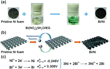 | ||
| Scheme 1 (a) Photographs of the synthesis processes of Bi/Ni, (b) schematic diagram of the synthesis route for Bi/Ni, and (c) redox potentials and chemical reaction of Ni and Bi3+. | ||
The as-synthesized Bi/Ni was characterized using X-ray diffraction (XRD). As shown in Fig. 1a, the characteristic diffraction peaks, corresponding to the facets of (012), (104), (110), (202), (024), and (122), are ascribed to the rhombohedral Bi (JCPDS No. 85-1329). The residual three diffraction peaks at 44.5°, 51.8°, and 76.4° are attributed to the face-centered cubic Ni. The formation of Bi/Ni in the replacement reaction was further confirmed using Raman spectroscopy in Fig. S1 (ESI†). Two typical peaks are observed in the Raman spectroscopy, which are assigned to the rocking and stretching vibrations of the Bi–Bi bonds, respectively.25 The scanning electron microscopy (SEM) image of Bi/Ni in Fig. 1b reveals that the uniform Bi nanoflakes of ∼100 nm in size and ∼25 nm in thickness are produced on the Ni foam. The d-spacing of Bi is estimated to be 0.33 nm in the high-resolution transmission electron microscopy (HRTEM) image in Fig. 1c, which matches well with its facet of (012) and is in good agreement with the XRD pattern in Fig. 1a. Moreover, the energy-dispersive X-ray spectroscopy (EDS) and elemental mappings of the Bi/Ni in Fig. 1d indicate a uniform distribution of Bi on the Ni foam. These results imply that uniform Bi nanoflakes are in situ produced on the Ni foam via the replacement reaction.
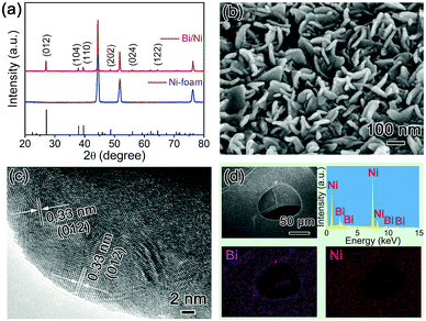 | ||
| Fig. 1 (a) XRD patterns of the as-synthesized Bi/Ni and pristine Ni foam, (b) SEM image, (c) high-resolution TEM image, and (d) EDS and elemental mappings of the Bi/Ni. | ||
The morphological evolution processes of the Bi/Ni were investigated by using SEM. Fig. 2a shows the SEM images of the Bi/Ni at different stages of the replacement reaction between Bi3+ and Ni foam for various reaction times. At the initial stage, the Bi atoms are reduced by the Ni nucleate on the smooth surface of the Ni foam, as shown in Fig. 2a, and then grow into Bi nanoseeds of ∼20 nm in size after 3 h, as shown in Fig. 2b. After the reaction for 6 h, as shown in Fig. 2c, the Bi nanoseeds develop into nanoflakes along the preferred orientation of the low-energy (012) plane.26,27 For the prolonged reaction for 18 h, the Bi grows by filling the void spaces between its nanoflakes, resulting in large blocks on the micrometer scale, as shown in Fig. 2d. This bottom-up growth process for Bi/Ni is schematically depicted in Fig. 2e. The growth of Bi starts from the surface of Ni foam when it contacts with Bi3+ ions. The Bi nanoseeds initiate the formation of Bi nanoflakes, and then thermodynamically evolve into large blocks after long-term submerging in the solution of Bi3+. The microstructure of Bi on Ni foam can also be tuned by the concentration of Bi3+, the reaction temperature and duration, as shown in Fig. S2 (ESI†).
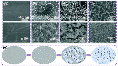 | ||
| Fig. 2 SEM images of the Bi/Ni at different react times: (a) pristine Ni foam, (b) 3 h, (c) 6 h, (d) 18 h; and (e) schematic diagram of the growth process of Bi/Ni. | ||
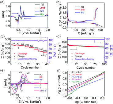
The as-synthesized Bi/Ni with nanoflakes was directly used as an electrode against Na metal with 1.0 M of NaPF6 in diethylene glycol dimethyl ether (DEGDME) as the electrolyte in coin cells. The mass loading of Bi is calculated to be 0.8–1.5 mg cm−2. Fig. 3a shows the typical cyclic voltammetry (CV) curves of the Bi/Ni electrode over the first 8 cycles from 0.1 to 2.0 V at a scan rate of 0.1 mV s−1. In the first cathodic scan, three reduction peaks are found at around 0.67, 0.47 and 0.38 V, which are ascribed to the gradual sodiation of Bi. This is different from the bulk Bi with one broad sodiation peak,19,21 in which the reduction peak at ∼0.41 V splits into two peaks at ∼0.47 and 0.38 V, as shown in Fig. 3a. This is speculated to be related to the two-dimensional structure of nanoflakes, as presented in Fig. 1b. The cathodic peaks in the following cycles shift positively and remain consistent over cycles. In the anodic scans, the two typical oxidation peaks at 0.61 and 0.78 V, corresponding to the desodiation and in agreement with the bulk Bi,21 are found to be overlapped. These results indicate the good cycling stability of the Bi/Ni electrode.
The first three galvanostatic discharge/charge curves of the Bi/Ni electrode at 20 mA g−1 are shown in Fig. 3b. In the discharge/charge processes, two plateaus are obtained to indicate two typical two-phase reactions beyond the first cycle. The discrepancy between the discharge/charge and CV curves is ascribed to the integrated nanoflake structure of the Bi/Ni electrode.19 Of note, the capacity ratio of the two plateaus in both discharge and charge processes is 1![[thin space (1/6-em)]](https://www.rsc.org/images/entities/char_2009.gif) :
:![[thin space (1/6-em)]](https://www.rsc.org/images/entities/char_2009.gif) 2, which is resulted from the gradual formation and decomposition of NaBi and Na3Bi in two distinct steps.11 The rate performance of the Bi/Ni electrode at varied current densities from 20 to 2000 mA g−1 is presented in Fig. 3c. It delivers reversible capacities of 377.1, 374.5, 359.1, 338.4, 318.0, 282, 239.7 and 206.4 mA h g−1 at 20, 40, 80, 200, 400, 800, 1200 and 2000 mA g−1, respectively. The corresponding discharge and charge profiles at each current density are shown in Fig. S3 (ESI†). The small polarization in the discharge/charge processes persisted with greatly increased current densities, which is attributed to the good electron conduction and electrolyte penetration in the integrated nanoflake structure of the Bi/Ni electrode. Furthermore, a high capacity of 302.4 mA h g−1 at 200 mA g−1 can be obtained after 100 cycles with a Coulombic efficiency of ∼100%, corresponding to a capacity retention of 89% in Fig. 3d. The electrochemical impedance spectroscopy (EIS) of the charged Bi/Ni electrode during cycles was measured, as shown in Fig. S4 (ESI†). It can be found that the resistance of the electrode is highly stable after the initial cycles, which is consistent with the discharge/charge profiles in Fig. 3. Such good rate capability and cycling stability of the Bi/Ni electrode are ascribed to the integrated nanoflake structure of the Bi/Ni electrode.
2, which is resulted from the gradual formation and decomposition of NaBi and Na3Bi in two distinct steps.11 The rate performance of the Bi/Ni electrode at varied current densities from 20 to 2000 mA g−1 is presented in Fig. 3c. It delivers reversible capacities of 377.1, 374.5, 359.1, 338.4, 318.0, 282, 239.7 and 206.4 mA h g−1 at 20, 40, 80, 200, 400, 800, 1200 and 2000 mA g−1, respectively. The corresponding discharge and charge profiles at each current density are shown in Fig. S3 (ESI†). The small polarization in the discharge/charge processes persisted with greatly increased current densities, which is attributed to the good electron conduction and electrolyte penetration in the integrated nanoflake structure of the Bi/Ni electrode. Furthermore, a high capacity of 302.4 mA h g−1 at 200 mA g−1 can be obtained after 100 cycles with a Coulombic efficiency of ∼100%, corresponding to a capacity retention of 89% in Fig. 3d. The electrochemical impedance spectroscopy (EIS) of the charged Bi/Ni electrode during cycles was measured, as shown in Fig. S4 (ESI†). It can be found that the resistance of the electrode is highly stable after the initial cycles, which is consistent with the discharge/charge profiles in Fig. 3. Such good rate capability and cycling stability of the Bi/Ni electrode are ascribed to the integrated nanoflake structure of the Bi/Ni electrode.
The Na+ transport properties of the Bi/Ni electrode are further studied by using CVs at different scan rates from 0.2 to 5 mV s−1, as displayed in Fig. 3e. They all exhibit three reduction peaks (R1, R2, and R3) and two oxidation peaks (O1 and O2), but R2 and R3 seem to merge as the scan rate is increased to 5 mV s−1. The relationship between the peak current (i) and the scan rate (v) can be described as i = avb, where a and b are positive variables. Typically, when b = 0.5, the electrochemical process is controlled by ion diffusion; and when b = 1, it is dominated by pseudocapacitance.24,28 As linearly fitted in Fig. 3f, the b values of the CV peaks of the Bi/Ni electrode are approximately 0.5, suggesting that the discharge/charge process is a Faradaic one and depends on the diffusion of Na+. The peak currents (i) of Fig. 3e are further plotted against the square roots of scanning rates, which complies with the Randles–Sevcik equation, as depicted in Fig. S5 (ESI†).29 Accordingly, the diffusion coefficients of DNa+(O1), DNa+(O2), DNa+(R1), DNa+(R2), and DNa+(R3) are calculated to be 2.01 × 10⁻¹⁰, 2.29 × 10⁻¹⁰, 0.66 × 10⁻¹⁰, 1.55 × 10⁻¹⁰, and 2.42 × 10⁻⁹ cm2 s−1, respectively. The high diffusion coefficients ensure the good rate performance and cyclic stability.
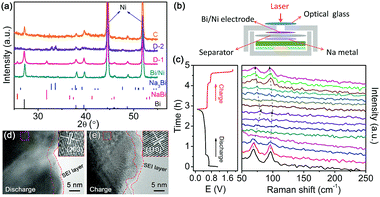
The sodiation/desodiation processes of the Bi/Ni electrode are understood by ex situ XRD, HRTEM, and in situ Raman spectroscopy, as displayed in Fig. 4. The crystalline structure evolution of Bi upon insertion/extraction of Na+ is monitored by XRD, as shown in Fig. 4a. When the electrode is discharged to 0.5 V (D-1), four new diffraction peaks at 25.7°, 31.8°, 36.6°, and 41.3° belonged to NaBi (JCPDS No. 65-2805) appear, in addition to those of Bi. After full discharge to 0.1 V (D-2), only the diffraction peaks at 32.9°, 33.7°, 39.3° and 47.7° are found, which are attributed to the new phase of Na3Bi (JCPDS No. 65-3525). The reversible formation of Bi after full charge is revealed by the XRD pattern (C) in Fig. 4a. Such sodiation/desodiation processes of Bi are further presented in an in situ cell in Fig. 4b and c, in which the reversible disappearance and re-appearance of the characteristic Raman bands of Bi are captured. This confirms the reversible reactions of Bi during discharge and charge, and agrees well with the XRD patterns in Fig. 4a. The discharged and charged products, Na3Bi and Bi, are confirmed by the well-developed facets of (203) and (110) in Fig. 4d and e, respectively. The thin films of the solid electrolyte interface (SEI) depicted in Fig. 4d and e are consistent with the limited irreversible capacity in Fig. 3b.30 Therefore, the electrochemical reaction mechanism of Bi during discharge and charge can be described as the following equations in two successive steps:
| Bi + Na+ + e− ↔ NaBi | (1) |
| NaBi + 2Na+ + 2e− ↔ Na3Bi | (2) |
In summary, we have successfully synthesized Bi nanoflakes integrated on Ni foam via replacement reactions. The 3D interconnected structure of the as-synthesized Bi/Ni can accommodate the huge volume change during sodiation and desodiation, and facilitate the diffusion of Na+ and electrolyte through the electrode. It is revealed that the Bi nanoflakes are sodiated and desodiated in two successive steps of Bi ↔ NaBi and NaBi ↔ Na3Bi. The Bi/Ni electrode exhibits attractive electrochemical performance for SIBs. Specifically, the electrode delivers 302.4 mA h g−1 after 100 cycles at 200 mA g−1 with a Coulombic efficiency of ∼100%, and good rate capability. The good electrochemical performance of the Bi/Ni is ascribed to the unique structure of Bi nanoflakes integrated on Ni foam. This investigation will shed light on the design and synthesis of integrated electrodes for high performance SIBs.
This work was supported by the National Key R&D Program of China (2017YFA0206700 and 2016YFB0901500), the National Natural Science Foundation of China (Grant No. 21603108 and 51671107), the 111 project of B12015, and the Natural Science Foundation of Tianjin (Grant No. 17JCQNJC06200).
Conflicts of interest
There are no conflicts to declare.References
- D. Kundu, E. Talaie and L. F. Nazar, Angew. Chem., Int. Ed., 2015, 54, 3431–3448 CrossRef CAS PubMed.
- J.-Y. Hwang, S.-T. Myung and Y.-K. Sun, Chem. Soc. Rev., 2017, 46, 3529–3614 RSC.
- Y. Li, Y.-S. Hu, M.-M. Titirici, L. Chen and X. Huang, Adv. Energy Mater., 2016, 6, 1600659 CrossRef.
- X. Han, F. Cheng, C. Chen, F. Li and J. Chen, Inorg. Chem. Front., 2016, 3, 866–871 RSC.
- Y. Zhao and A. Manthiram, Chem. Commun., 2015, 51, 13205–13208 RSC.
- J. Mao, X. Fan, C. Luo and C. Wang, ACS Appl. Mater. Interfaces, 2016, 8, 7147–7155 CAS.
- H. Xie, W. P. Kalisvaart, B. C. Olsen, E. J. Luber, D. Mitlin and J. M. Buriak, J. Mater. Chem. A, 2017, 5, 9661–9670 CAS.
- Y. Liu, N. Zhang, L. Jiao and J. Chen, Adv. Mater., 2015, 27, 6702–6707 CrossRef CAS PubMed.
- Y. Zhao and A. Manthiram, Chem. Mater., 2015, 27, 3096–3101 CrossRef CAS.
- J. W. Wang, X. H. Liu, S. X. Mao and J. Y. Huang, Nano Lett., 2012, 12, 5897–5902 CrossRef CAS PubMed.
- L. D. Ellis, B. N. Wilkes, T. D. Hatchard and M. N. Obrovac, J. Electrochem. Soc., 2014, 161, A416–A421 CrossRef CAS.
- Z. Liu, X.-Y. Yu, X.-W. Lou and U. Paik, Energy Environ. Sci., 2016, 9, 2314–2318 CAS.
- S. Liu, Z. Luo, J. Guo, A. Pan, Z. Cai and S. Liang, Electrochem. Commun., 2017, 81, 10–13 CrossRef CAS.
- M. Moradi, Z. Li, J. Qi, W. Xing, K. Xiang, Y.-M. Chiang and A. M. Belcher, Nano Lett., 2015, 15, 2917–2921 CrossRef CAS PubMed.
- L. Liang, Y. Xu, H. Dong, M. Zhou, H. Zhao, U. Kasier and Y. Lei, J. Mater. Chem. A, 2017, 5, 1749–1755 CAS.
- S. A. Webb, L. Baggetto, C. A. Bridges and G. M. Veith, J. Power Sources, 2014, 248, 1105–1117 CrossRef CAS.
- Y. Shao, M. Gu, X. Li, Z. Nie, P. Zuo, G. Li, T. Liu, J. Xiao, Y. Cheng, C. Wang, J.-G. Zhang and J. Liu, Nano Lett., 2014, 14, 255–260 CrossRef CAS PubMed.
- S. Liu, J. Feng, X. Bian, J. Liu and H. Xu, J. Mater. Chem. A, 2016, 4, 10098–10104 CAS.
- J. Sottmann, M. Herrmann, P. Vajeeston, Y. Hu, A. Ruud, C. Drathen, H. Emerich, H. Fjellvåg and D. S. Wragg, Chem. Mater., 2016, 28, 2750–2756 CrossRef CAS.
- D. Su, S. Dou and G. Wang, Nano Energy, 2015, 12, 88–95 CrossRef CAS.
- C. Wang, L. Wang, F. Li, F. Cheng and J. Chen, Adv. Mater., 2017, 29, 1702212 CrossRef PubMed.
- K. Liao, T. Zhang, Y. Wang, F. Li, Z. Jian, H. Yu and H. Zhou, ChemSusChem, 2015, 8, 1429–1434 CrossRef CAS PubMed.
- A. J. Bard, R. Parsons and J. Jordan, Standard Potentials in Aqueous Solution, CRC Press, New York, 1985 Search PubMed.
- L. Wang, C. Wang, N. Zhang, F. Li, F. Cheng and J. Chen, ACS Energy Lett., 2017, 2, 256–262 CrossRef CAS.
- K. Trentelman, J. Raman Spectrosc., 2009, 40, 585–589 CrossRef CAS.
- V. Bansal, H. Jani, J. Du Plessis, P. J. Coloe and S. K. Bhargava, Adv. Mater., 2008, 20, 717–723 CrossRef CAS.
- S. Kim, W. J. Dong, S. Gim, W. Sohn, J. Y. Park, C. J. Yoo, H. W. Jang and J.-L. Lee, Nano Energy, 2017, 39, 44–52 CrossRef CAS.
- K. Zhang, M. Park, L. Zhou, G.-H. Lee, J. Shin, Z. Hu, S.-L. Chou, J. Chen and Y.-M. Kang, Angew. Chem., Int. Ed., 2016, 55, 12822–12826 CrossRef CAS PubMed.
- J. J. Van Benschoten, J. Y. Lewis, W. R. Heineman, D. A. Roston and P. T. Kissinger, J. Chem. Educ., 1983, 60, 772–776 CrossRef CAS.
- B. Zhang, G. Rousse, D. Foix, R. Dugas, D. Corte and J.-M. Tarascon, Adv. Mater., 2016, 28, 9824–9830 CrossRef CAS PubMed.
Footnote |
| † Electronic supplementary information (ESI) available: Experimental details, Raman spectra, SEM images, discharge/charge curves, EIS spectra, and plot of peak currents (ip) vs. square roots of scanning rates of the CVs and the corresponding linear fittings of Bi/Ni. See DOI: 10.1039/c7cc08341f |
| This journal is © The Royal Society of Chemistry 2018 |

