
 Open Access Article
 This Open Access Article is licensed under a
 Creative Commons Attribution 3.0 Unported Licence
Transparent conducting n-type ZnO:Sc – synthesis, optoelectronic properties and theoretical insight†
Sebastian C.
Dixon
 a,
Sanjayan
Sathasivam
a,
Benjamin A. D.
Williamson
b,
David O.
Scanlon
bc,
Claire J.
Carmalt
a and
Ivan P.
Parkin
*a
a,
Sanjayan
Sathasivam
a,
Benjamin A. D.
Williamson
b,
David O.
Scanlon
bc,
Claire J.
Carmalt
a and
Ivan P.
Parkin
*a
aMaterials Chemistry Centre, Department of Chemistry, University College London, 20 Gordon Street, London WC1H 0AJ, UK. E-mail: i.p.parkin@ucl.ac.uk; Fax: +44 (0)20 769 7463; Tel: +44 (0)20 7679 4669
bKathleen Lonsdale Materials Chemistry, Department of Chemistry, University College London, 20 Gordon Street, London WC1H 0AJ, UK
cDiamond Light Source Ltd, Diamond House, Harwell Science and Innovation Campus, Didcot, Oxfordshire OX11 0DE, UK
First published on 19th July 2017
Abstract
A joint theoretical-experimental study has been carried out for Sc-doped ZnO (SZO), one of the lesser-studied n-type transparent conducting oxide materials. Density functional theory has been used to create a computational model of SZO, in order to provide a theoretical basis for experimentally-observed phenomena where growth conditions, dopability and electronic properties are concerned. Meanwhile a range of thin films of SZO have been synthesised via chemical vapour deposition in an attempt to (i) observe experimentally the theoretically predicted properties, thereby providing mutual validation of the studies; (ii) seek the optimum dopant quantity for minimal electrical resistivity, and; (iii) demonstrate that transparent and electrically conductive SZO can be synthesised by chemical vapour deposition means. The films exhibit resistivities as low as ρ = 1.2 × 10⁻³ Ω cm, with carrier density n = 7.2 × 1020 cm−3 and charge carrier mobility μ = 7.5 cm2 V−1 s−1. Low resistivity of the films was retained after 12 months in storage under ambient conditions, indicating strong atmospheric stability. The films exhibit a high degree of transparency with 88% transmission in the visible range (400–750 nm). A correction to the Tauc method was applied to estimate band gaps of Eoptg = 3.45 ± 0.03 eV in the most conductive SZO sample and Eoptg = 3.34 ± 0.03 eV in nominally undoped ZnO.
1. Introduction
Transparent conducting oxide (TCO) thin films are widely adopted in optoelectronic devices as transparent electrodes. The unique properties of these indispensable materials are unusual by traditional principles; the wide band gap required for optical transparency (Eg > 3.1 eV) which separates the valence band (VB) from the conduction band (CB) leads to highly resistive semiconductor behaviour in pure stoichiometric ZnO, due to the low probability of electron excitation across this threshold. However, doping of the material offers a solution to this dilemma; extrinsic doping by artificial introduction of substitutional impurities such as Al(III)1 or Ga(III)2 on Zn(II) crystallographic sites results in an effective local excess of electrons at the defect sites. This produces an electron donor level close to the CB minimum (CBM), which facilitates donation of electrons into the CB to confer electrical conductivity to the material whilst the wide optical band gap is retained. In this way, it is possible to synthesise transparent and conducting inorganic materials such as ZnO:(Al,1 Ga,2 F,3 Sc4) and SnO2:F5 by extrinsic doping of the semiconductor.6 The most widely used TCO material is In2O3:Sn (ITO), which is a high-performance material demonstrating high optical transmission in the visible (>90% at 550 nm) and low electrical resistivities (ρ = 10−4 − 10−5 Ω cm).7 However, due to its low natural abundance and localised geological distribution, the commercial supply of indium is expensive and in a perpetual state of risk, which is problematic for various reasons.8 As such, it has naturally become desirable to seek an alternative to ITO as a commercial TCO, which is evident from the amount of research dedicated to this end in recent years.Computational modelling of potential TCO systems has become an important and indispensable method for their high-throughput screening,9 often working side-by-side with experimental synthesis work to quickly seek ideal doping scenarios and provide a more complete picture of the origin of observable physical properties.10 While Al-doped and Ga-doped ZnO have received much attention as extrinsically n-type doped ZnO systems in recent years, reports on other trivalent dopants are reported considerably less often. In particular, Sc-doped ZnO (SZO) has shown promise as an alternative TCO material with low resistivity and high visible transmittance,4,11 however with relatively few deposition studies having been carried out and still fewer theoretical studies developing an understanding of this material. Development of a computational model to describe the behaviour of Sc doping in ZnO is crucial to achieving this. The present work represents the first such instance, in which density functional theory has been applied to construct a theoretical model of the doping behaviour of Sc in ZnO. The theoretical model is developed alongside a strongly correlated experimental synthesis of ZnO:Sc via aerosol-assisted chemical vapour deposition.
Chemical vapour deposition (CVD) is a commonly adopted means by which to achieve deposition of TCO thin films, which is performed by delivery of a well-mixed vapour containing precursors of the host and dopant oxides to the heated substrate, whereupon thermal decomposition occurs to yield the desired material from the vapour. Traditional CVD, usually referred to as thermal, metal–organic or atmospheric-pressure CVD (APCVD), generates these vapours from thermal heating of volatile precursors such as diethyl zinc3 with an oxygen source such as ethanol and a dopant source such as trifluoroethanol (in the case of F-doped ZnO deposition).3 However, in order for this technique to be effective there is a fundamental requirement that the (often liquid) precursor has an appreciable vapour pressure, which, aside from restricting the scope of precursor selection for a given target material, also naturally leads to precursors with inherent hazards such as flammability, pyrophoricity, explosivity, corrosivity and respiratory and environmental toxicity. This leads to obvious complications regarding their transport, storage, usage and disposal.12 Such considerations have given rise to a more versatile method of CVD in recent years known as aerosol-assisted CVD (AACVD), in which a solution of the precursor is aerosolised in order to generate the vapour.13 This alternative enables use of a much more diverse range of potential precursors, whose only requirements are: (a) that the precursor decomposes below the set deposition temperature to yield the desired material, and (b) that the precursor is soluble in a suitable solvent (e.g. methanol, chloroform, toluene).12 As such, a popular choice for AACVD precursor selection is an inorganic or organic salt of the desired element such as indium chloride or zinc acetate (in the case of ZnO:In films),14 which is often cheap, readily available and usually comes with fewer significant associated physical hazards compared to its volatile liquid counterpart. In addition to this, AACVD permits ‘one-pot’ depositions, where precursors with similar solubility can be dissolved in a common solvent and deposited together from a single precursor flask. Such a method is ideal for doping studies, where it is desirable to produce a well-mixed vapour with a highly controllable chemical composition. As such, it is the method of choice in the present study for Sc-doping of ZnO.
2. Methodology
2.1. Materials
Zinc(II) acetate ([Zn(OAc)2]) and scandium(III) acetate ([Sc(OAc)3]) were obtained from Sigma-Aldrich. Nitrogen carrier gas (N2, 99.99%) was obtained from BOC. Methanol (99.5%) was obtained from Merck Millipore. All of the above chemicals were used as supplied. Float glass with a 25 nm SiO2 barrier layer was provided by NSG Pilkington Ltd and cut manually into substrates (50 × 145 × 4 mm).2.2. Experimental procedure
In a typical deposition, zinc(II) acetate (0.69 g, 3.0 mmol) was dissolved in methanol (35 mL) with stirring. Scandium(III) acetate was dissolved in a minimum volume of deionised water (ca. 5 mL) with swirling. The methanol solution was added to the aqueous solution followed by stirring for ca. 10 min. Varying molar ratios of the Sc to Zn precursor were used to deposit a range of films with varying Sc content. In the 3 mol% Sc:Zn film, the amount of scandium(III) acetate to use (0.021 g, 0.090 mmol) was calculated from the amount of zinc(II) acetate in the solution. Precursor solutions containing 0.0, 1.0, 2.0, 3.0 and 4.0 mol% Sc:Zn content were prepared in this manner. Higher proportions of aqueous Sc precursor presented miscibility issues with the alcoholic Zn precursor solution, therefore placing an upper limit to the quantity of dopant deliverable by this method.The precursor solution was transferred to a glass AACVD bubbler for deposition. Silica barrier glass substrates were cleaned prior to deposition with detergent, isopropyl alcohol and acetone, whereupon they were positioned atop a graphite block within the cold-walled horizontal-bed reactor chamber. The graphite block contained a Whatman cartridge heater regulated by a Pt–Rh thermocouple. A sheet of stainless steel (45 × 150 mm) was supported at a height of 8 mm above the substrate to assist with laminar flow of the precursor aerosol over the substrate. This arrangement was enclosed by a quartz tube. Polytetrafluoroethylene tubing (PTFE, 8 mm internal diameter) served to deliver the aerosol from the precursor vessel to a brass baffle manifold which homogenised the flow of aerosol into the attached reaction chamber. Nitrogen carrier gas was passed throughout, arriving first at the precursor vessel then travelling along the tubing, through the baffle and into the reactor chamber between the glass and copper plates, then at last out of the far exhaust. The nitrogen was allowed to flow in this way for ca. 10 min prior to aerosolisation of the precursor in order to allow for equilibration of the deposition environment. The reaction chamber was heated at a rate of 15 °C min−1 to its target temperature of 600 °C, at which point aerosolisation of the precursor was commenced using a Johnson Matthey Liquifog® piezoelectric ultrasonic humidifier approximately half-filled with deionised water. The carrier gas transported the aerosol at a fixed rate of 2.0 L min−1. The deposition process was allowed to proceed in this manner until all of the precursor solution had been aerosolised, at which point the humidifier and heating elements were shut off and the substrate allowed to cool under continual flow of nitrogen. Once the reactor had reached below 100 °C, the samples were removed from the reactor and handled in air.
2.3. Characterisation details
X-ray diffractometry was conducted at glancing angle (θ = 0.8°) in air using a Bruker D8 Discover diffractometer in the range 2θ = 10–66° with monochromatic Cu Kα1 and Kα2 radiation (1.54056 and 1.54439 Å respectively) under voltage 40 kV and current 40 mA. X-ray photoelectron spectroscopy was conducted using a Thermo Scientific K-alpha spectrometer with monochromated Al Kα radiation (1486.68 eV), a dual-beam charge compensation system and a constant pass energy of 50 eV with spot size 400 μm. Survey scans were collected for the binding energy range 0–1200 eV. Data was calibrated against C 1s (284.5 eV) and fitted using CASA XPS software. UV-visible spectra were taken using a Perkin Elmer Lambda 950 UV/Vis/NIR Spectrophotometer in transmission mode. A Labsphere reflectance standard was used as a reference. Scanning electron microscopy was conducted on a JEOL 6700F SEM using an acceleration voltage of 20 kV, with an attached Oxford Instruments INCA Energy EDXA system operated at 15 kV. Hall effect measurements were taken using the Van der Pauw four-point probe configuration at room temperature to measure the resistivity of the films, their free charge carrier concentrations and mobilities. Measurements were performed using an Ecopia HMS-3000 instrument with a 0.58 T permanent magnet and a current of 1 mA, using square-cut coupons (ca. 1 × 1 cm) of the deposited films. Silver paint obtained from Agar Scientific was used at each of the four corners on the films to enhance Ohmic contact between the Au electrodes and the film. Thermogravimetric analysis (TGA) and differential scanning calorimetry (DSC) were performed under helium using a Netzsch STA 449 C Jupiter Thermo-microbalance in an open aluminium oxide crucible.2.4. Computational methodology
All density functional theory (DFT) calculations were carried out using the Vienna ab initio simulation package (VASP).15–18 Within this code a plane-wave basis set is used to describe the valence electronic states and the projector-augmented wave (PAW)19 method which maps the core electrons (treated with pseudopotentials) onto the valence electrons (treated explicitly) for computational efficiency, giving results akin to an all electron method. ZnO crystallises in the wurtzite crystal structure (P63mc). In order to counteract the self-interaction error (SIE) and thus band gap errors typical to standard DFT functionals, the hybrid functional Heyd–Scuzeria–Ernzerhoff (HSE)20 was employed for all calculations.Hybrid functionals improve on standard functionals in improving geometric and electronic structure compared to experiment.21–41 Standard DFT functionals such as generalised gradient approximation (GGA) or local density approximation (LDA) fall short in their description of the self-interaction error which typically leads to underestimated band gaps, this is known to affect the defect thermodynamics.42–44 The HSE06 approach adds 25% of HF exchange (α = 0.25) however HSE with 37.5% exchange has been reported to yield geometric and electronic structures in good agreement with experiment.30,45
The lattice parameters (a, b, c), enthalpy of formation (ΔHf) and band gap (Edirg) for bulk ZnO compared to experiment and other DFT studies are shown in Table 1. It is clear that using HSE with 37.5% HF exchange gives structural, electronic and thermodynamic results closest to experimental low temperature studies.45–48 The direct fundamental band gap (Edirg) calculated in this work matches to within 1.5% of the experimentally defined band gap for ZnO, similar to the study carried out by Oba et al.30 which also used 37.5% HF exchange. The enthalpy of formation (ΔHf) also matches the experimental value to within 10% despite the calculations being carried out at the athermal limit (T = 0 K).
In order to simulate the effect of intrinsic defects and extrinsic dopants in ZnO, a 3 × 3 × 2 supercell containing 72 atoms was created. Each calculation was spin polarised and the ions were relaxed using an energy cutoff of 450 eV and a 2 × 2 × 2 Γ-centred k-point mesh. When the forces on all the atoms were less than 0.01 eV, the system was deemed to be converged.
 | (1) |
| μZn + μO = ΔHZnOf = −3.25 eV | (2) |
The Zn-rich/O-poor conditions (which typically favour the formation of n-type defects) are determined by the formation of metallic Zn i.e. ΔμZn = 0; ΔμO = −3.25 eV. Likewise for Zn-poor/O-rich conditions (where p-type defect formation is favoured) the limit is determined by the formation of O2 gas, ΔμO = 0; ΔμZn = −3.25 eV. Alongside this, the solubilities of the dopant-related species are limited by the formation of the secondary phase Sc2O3, as shown in eqn (3), while the limited solubility of Sc in ZnO has also been noted in previous experimental study.55 Therefore, under Zn-poor/O-rich conditions and O-poor/Zn-rich conditions the Sc chemical potentials can be calculated to be ΔμSc = −9.75 eV and ΔμSc = −4.87 eV respectively. It should be noted that the uppermost dopant quantity used in this study represents the miscibility limit of the aqueous Sc precursor with the methanolic Zn precursor in the one-pot precursor vial, rather than the chemical solubility limit described here.
 | (3) |
The thermodynamic transition (ionisation) levels of a given defect illustrate the Fermi level position at which that defect changes from charge state q to q′, which is calculated as per eqn (4). These transition levels are shown in Fig. 3. These ionisation levels are experimentally important as they can be observed using techniques such as deep level transient spectroscopy (DLTS).
 | (4) |
3. Results and discussion
3.1. Computational study
The density of states (DOS) and band structure for bulk ZnO are shown in Fig. 1 and 2 respectively. In the DOS, the VBM is predominantly made up of O 2p states with some Zn p and d mixing, typical of wide band gap metal oxide semiconductors such as In2O3, SnO2, TiO2 and BaSnO3.41,56,57 The CBM is made up of primarily Zn s states with O s and p states. The band structure shown of ZnO displays a direct band gap at Γ (3.39 eV) with the characteristically highly disperse CBM. The effective electron mass is ca. 0.27 me in both the Γ–K and Γ–M directions, which compares well with experimental values of 0.28 me.58 There is also a large CBM to CBM + 1 intraband spacing (ca. 4 eV) present allowing for the accommodation of extra charge carriers whilst retaining the high optical transparency.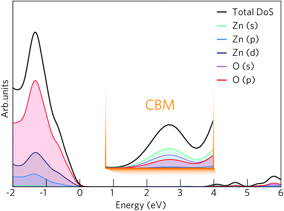 | ||
| Fig. 1 The calculated density of states (DOS) for ZnO shown with an expanded view of the conduction band minimum (CBM) inset. The VBM is centred at 0 eV. | ||
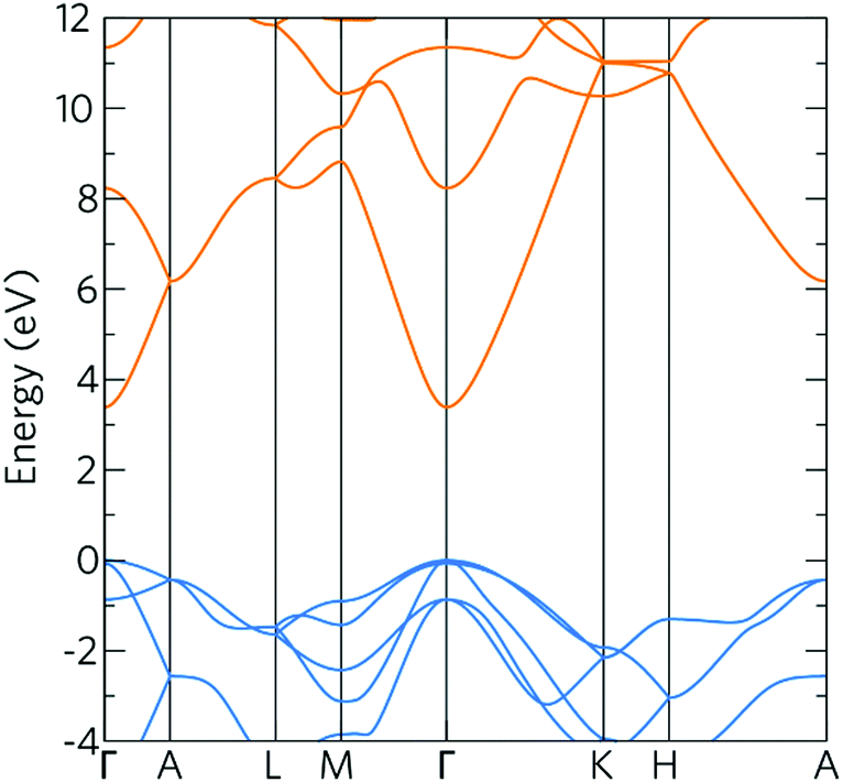 | ||
| Fig. 2 The calculated band structure for bulk ZnO, calculated using the HSE hybrid functional with 37.5% HF exchange. The valence bands are indicated in blue and the conduction bands in orange. The valence band maximum is set to 0 eV. | ||
Fig. 3 shows defect formation energies within Sc-doped ZnO as a function of Fermi energy position under (a) Zn-rich/O-poor and (b) Zn-poor/O-rich conditions. Under typical n-type conditions (Zn-rich/O-poor), the formation energies of positively charged defects should be lower in energy than those of negatively charged defects. Under these conditions the dominant intrinsic donor defect is VO at Fermi energies just below the CBM which acts as a deep donor (i.e. the 2+/0 transition level occurs ca. 1.15 eV below the CBM) which is consistent with experimental and theoretical studies alike,30,32,49,59–64 meaning that VO does not contribute to the conductivity of ZnO. This type of “negative U” type behaviour of VO in wide band gap TCOs is well known.21 The high conductivity of “undoped” ZnO has since been attributed to the presence of unintentional hydrogen doping from synthesis forming a shallow donor state below the CBM at formation energies as low as VO and has been confirmed experimentally using muon spectroscopy.30,65,66 However, the ScZn defect appears to possess a somewhat significant formation energy (ca. 1.55 eV at the CBM) while acting as a resonant donor, injecting its excess electron directly into the conduction band. Importantly, this defect does not seem to be compensated for by any intrinsic acceptor defects until well above the CBM under these growth conditions. From this it is expected that incorporation of a high concentration of Sc would be quite difficult under equilibrium conditions, indicating that non-equilibrium growth techniques such as molecular beam epitaxy (MBE) or sputtering could be sensible methods to achieve a higher level of doping. The VZn intrinsic defect states are very high in energy and as such concentrations of this defect will be negligible under these conditions (the formation energy of the neutral charge state is ca. 6.97 eV which compares well with the hybrid DFT work carried out by Oba et al.30 and with LDA work by Van de Walle and coworkers49). Scint also acts as a shallow donor, however under Zn-rich/O-poor conditions we can see it has a particularly high formation energy. Therefore, Sc will be incorporated preferentially on the Zn site, such that occurrence of Scint is unlikely in the AACVD samples prepared here.
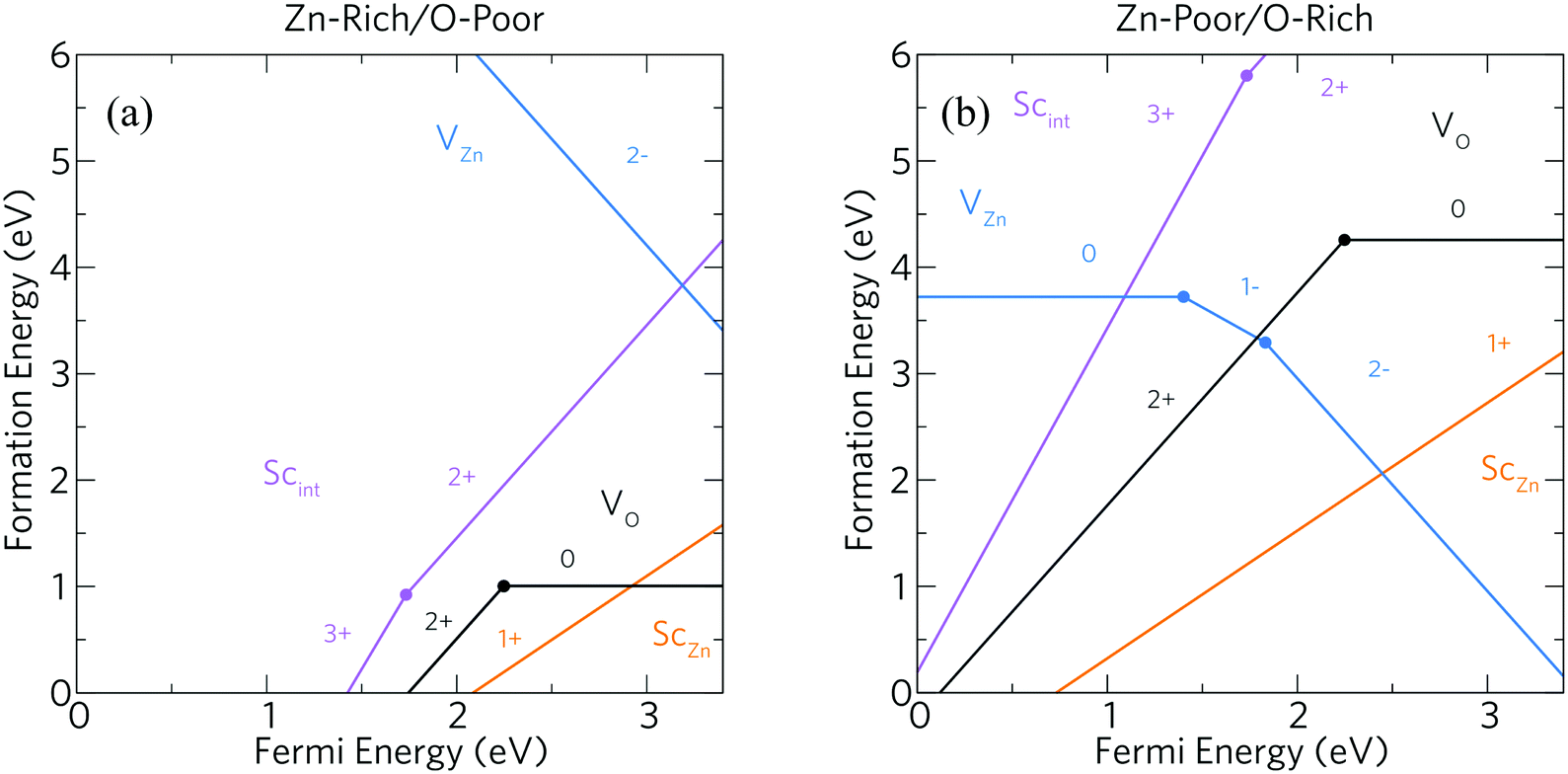 | ||
| Fig. 3 Calculated formation energies as a function of Fermi energy for intrinsic defects (VO, black and VZn, blue) alongside Sc dopant states, substitutional ScZn (orange) and interstitial Scint (pink) under (a) Zn-rich/O-poor and (b) Zn-poor/O-rich conditions. The solid dots indicate the transition levels ε(q/q′). | ||
Fig. 3(b) displays the Zn-poor/O-rich conditions favouring the growth of acceptor defects and has the effect of pushing the donor defects (VO, ScZn and Scint) higher in energy. Here, the formation energy of the neutral charge state of VZn is reduced and is shown to be a deep acceptor with the 0/1-transition level appearing at ca. 1.5 eV above the VBM, at a relatively high formation energy of ca. 3.7 eV. The 1-/2-transition state level occurs ca. 1.8 eV above the VBM with a formation energy of ca. 3.3 eV. These results are in contrast to the transition levels calculated in other theoretical works which shows the 0/1- and 1-/2-levels to occur ca. 0.8 eV and ca. 2.5 eV above the VBM respectively with formation energies of ca. 4 eV and ca. 2 eV.30,40,49,60 Our calculations propose that the 0/1-transition level is 0.7 eV deeper than previously thought whereas the 1-/2-level is in fact shallower by ca. 0.7 eV. One plausible reason for the deeper acceptor levels in our calculations is due to the correct description of hole localisation on the neighbouring O atoms as shown in Fig. 4; (a) shows the localisation of two holes for the neutral charge state of VZn, and (b) shows the removal of one hole to form the 1-charge state. This localisation is important for correct lattice relaxation and therefore affects the total energy of the system.67 This reduces the neutral vacancy and 1-charge state pushing the transition state energies deeper into the band gap. The only work found where this hole localisation is addressed is in work by Clark et al., where calculations using a “screened exchange” functional show a small localisation on the 1-charge state, however this localisation is small and which will not change the thermodynamic picture much from previous works.40
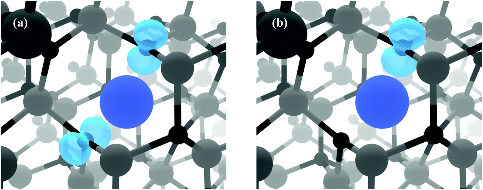 | ||
| Fig. 4 A close up view of the VZn for (a) the neutral charge state and (b) the 1-charge state. These diagrams show the localised holes (blue charge isosurface with a density of 0.02 eV Å−1) associated with the deep VZn states. The Zn vacancy is shown by the large blue sphere, whilst Zn and O atoms are depicted as grey and black spheres respectively. | ||
Under Zn-poor/O-rich conditions, ScZn is the dominant donor defect close to the CBM but is fully compensated for by VZn, thereby pinning the Fermi level ca. 0.9 eV below the CBM; as such, under these conditions no favourable scandium doping will be achieved. Thus, it is clear that Sc-doped ZnO samples grown close to the limit of O-rich conditions will be insulating, and some degree of O-poor conditions are necessary to achieve efficient n-type conductivity.
3.2. Synthesis and characterisation
Thermogravimetric analysis (TGA) and differential scanning calorimetry (DSC) were carried out under helium on the [Sc(OAc)3] precursor in order to observe its response to the temperatures applied in the deposition. The TGA shown in Fig. 5 indicates that the [Sc(OAc)3] begins to decompose towards Sc2O3 at around 300 °C, with the transition largely complete by around 380 °C. DSC indicates that this decomposition is sharply endothermic, and seems to feature an overlapping between a peak at 340 °C and a stronger peak at 360 °C, while a weaker endothermic feature is also apparent at 500–600 °C. While a previous study of the thermal decomposition of [Sc(OAc)3] is difficult to find, the thermal decomposition of rare earth metal acetates ([Ln(OAc)3]) is well-documented.68 Assuming a similar decomposition pathway for [Sc(OAc)3], these endothermic stages can be ascribed to the following processes:| 2[Sc(OAc)3] → Sc2(CO3)3 + 3CH3COCH3 at 340 °C; |
| Sc2(CO3)3 → Sc2O3·CO2 + 2CO2 at 360 °C, then; |
| Sc2O3·CO2 → Sc2O3 + CO2 at 500–600 °C. |
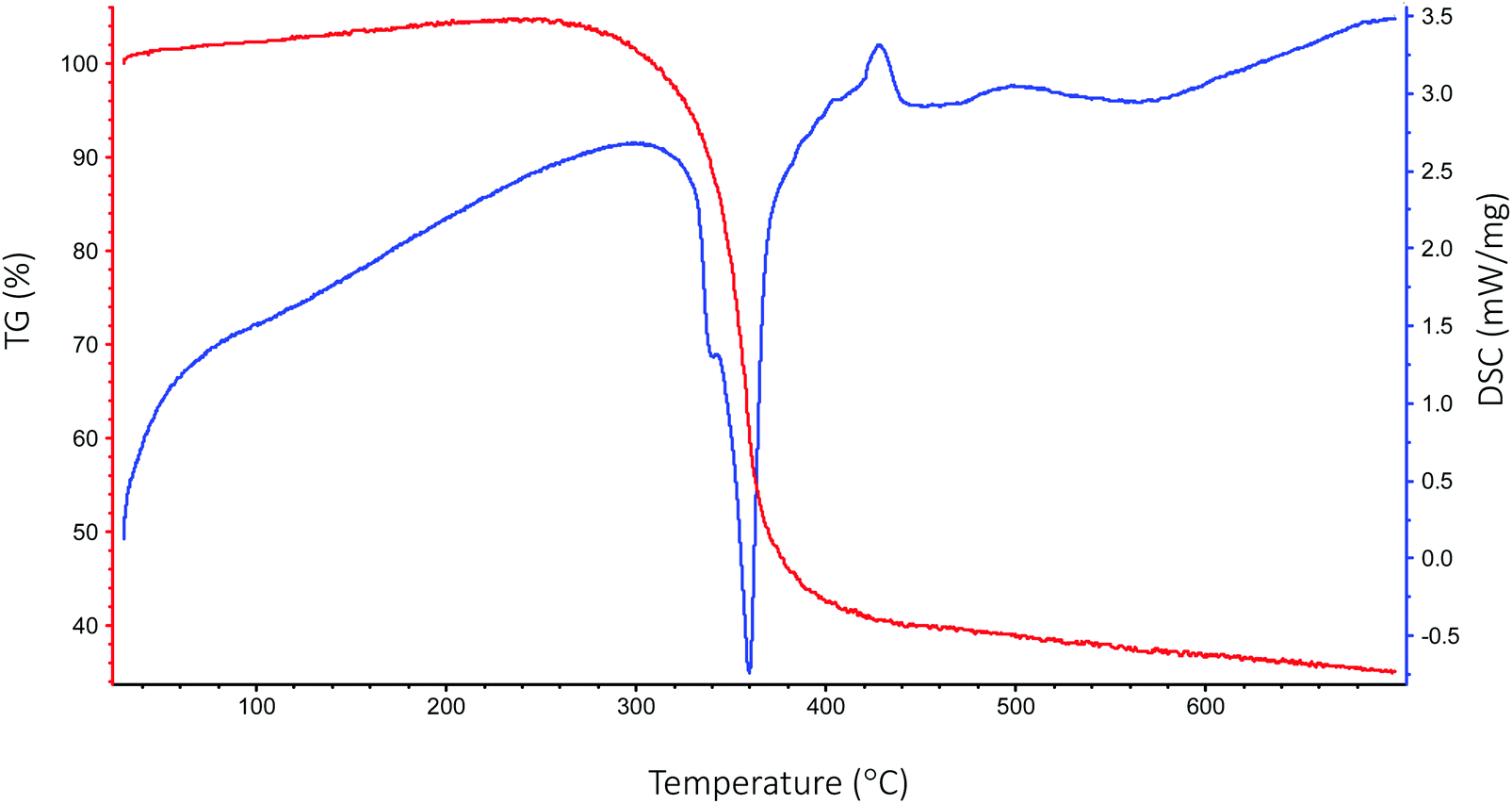 | ||
| Fig. 5 TGA and DSC curves of the [Sc(OAc)3] precursor obtained under helium. | ||
A similar result has also previously been observed in the thermal decomposition of scandium formate ([Sc(HCO2)3]), which also followed an endothermic decomposition pathway leading through an intermediate Sc2O3·CO2 formed at 380 °C accompanied by an outgassing of CO2, followed by a more gradual outgassing of CO2 at higher temperature.69 As for the [Zn(OAc)2] precursor, previous study has found that this decomposes in an exothermic reaction around 300 °C.70
Zinc oxide thin films incorporating a range of Sc dopant concentrations were deposited via AACVD from one-pot precursor solutions containing Zn(II) and Sc(III) acetates in a methanol–water solvent mixture. The films adhered strongly to the substrate, fully resisting removal by a steel scalpel and by Scotch® tape. Bottom-plate deposition occurred to yield the hexagonal wurtzite films which were visibly transparent and electrically conductive.
The films were analysed for their elemental content via energy-dispersive X-ray spectroscopy (EDX) and X-ray photoelectron spectroscopy (XPS). In the XPS (local and survey scans shown in Fig. S1 in ESI†), the Sc 2p and Zn 2p environments were probed. The Zn 2p3/2 peak occurred at 1021.3 eV at low doping levels, agreeing with the 1021.5 eV obtained for ZnO thin films deposited via AACVD in previous studies.71 This blue-shifted slightly to 1021.4 eV for films with bulk Sc doping over 1 at% relative to Zn (as determined by EDX). Zn(II) and Sc(III) were revealed as being the only oxidation states present, with no occurrence of metallic Zn(0) or Sc(0). It should be noted that the apparent shoulder at 398 eV occurring adjacent to the Sc(III) peaks arises from the N 1s environment.
The efficiency of dopant incorporation for the thin film fabrication was calculated to be 42 ± 6% (where 6% is the standard error), from the bulk Sc![[thin space (1/6-em)]](https://www.rsc.org/images/entities/char_2009.gif) :Zn ratios for all films as obtained from EDX measurements, and the ratio of Sc and Zn precursors in the initial mixtures. It is unsurprising that the quantity of Sc going into the films is consistently lower than ‘expected’ from the precursor ratios, given that the Sc(OAc)3 precursor decomposes at a higher temperature than Zn(OAc)2; it ought to therefore be expected that at a given deposition temperature, the Zn precursor decomposes faster than the Sc precursor, such that the quantity of Sc being incorporated into the film is proportional, but not equivalent to, the ratio of Sc to Zn precursors in the aerosol. As such, this particular measurement is unique to this synthesis, i.e. in which acetates of Sc(III) and Zn(II) are combined in a one-pot water–methanol mixture and deposited under nitrogen onto a 600 °C barrier glass substrate, etc. The incorporation efficiency of 42 ± 6% therefore does not necessarily apply to other methods for Sc-doping of ZnO.
:Zn ratios for all films as obtained from EDX measurements, and the ratio of Sc and Zn precursors in the initial mixtures. It is unsurprising that the quantity of Sc going into the films is consistently lower than ‘expected’ from the precursor ratios, given that the Sc(OAc)3 precursor decomposes at a higher temperature than Zn(OAc)2; it ought to therefore be expected that at a given deposition temperature, the Zn precursor decomposes faster than the Sc precursor, such that the quantity of Sc being incorporated into the film is proportional, but not equivalent to, the ratio of Sc to Zn precursors in the aerosol. As such, this particular measurement is unique to this synthesis, i.e. in which acetates of Sc(III) and Zn(II) are combined in a one-pot water–methanol mixture and deposited under nitrogen onto a 600 °C barrier glass substrate, etc. The incorporation efficiency of 42 ± 6% therefore does not necessarily apply to other methods for Sc-doping of ZnO.
Elemental analysis also indicated a stronger presence of Sc at the surface than in the bulk, as evident in the XPS depth profile shown in Fig. 6. It is likely that surface Sc(III) corresponds to both substitutional ScZn dopant environments and an amorphous secondary phase Sc2O3, which has been observed to nucleate at the ZnO grain boundaries in previous studies72 and which our theoretical model indicates competes with substitutional ScZn as Sc loading increases (see Section 2.4.2). Such a nucleation results in a decrease in grain size with increasing dopant concentration due to competing growth processes, which was observed in the SEM (vide infra).
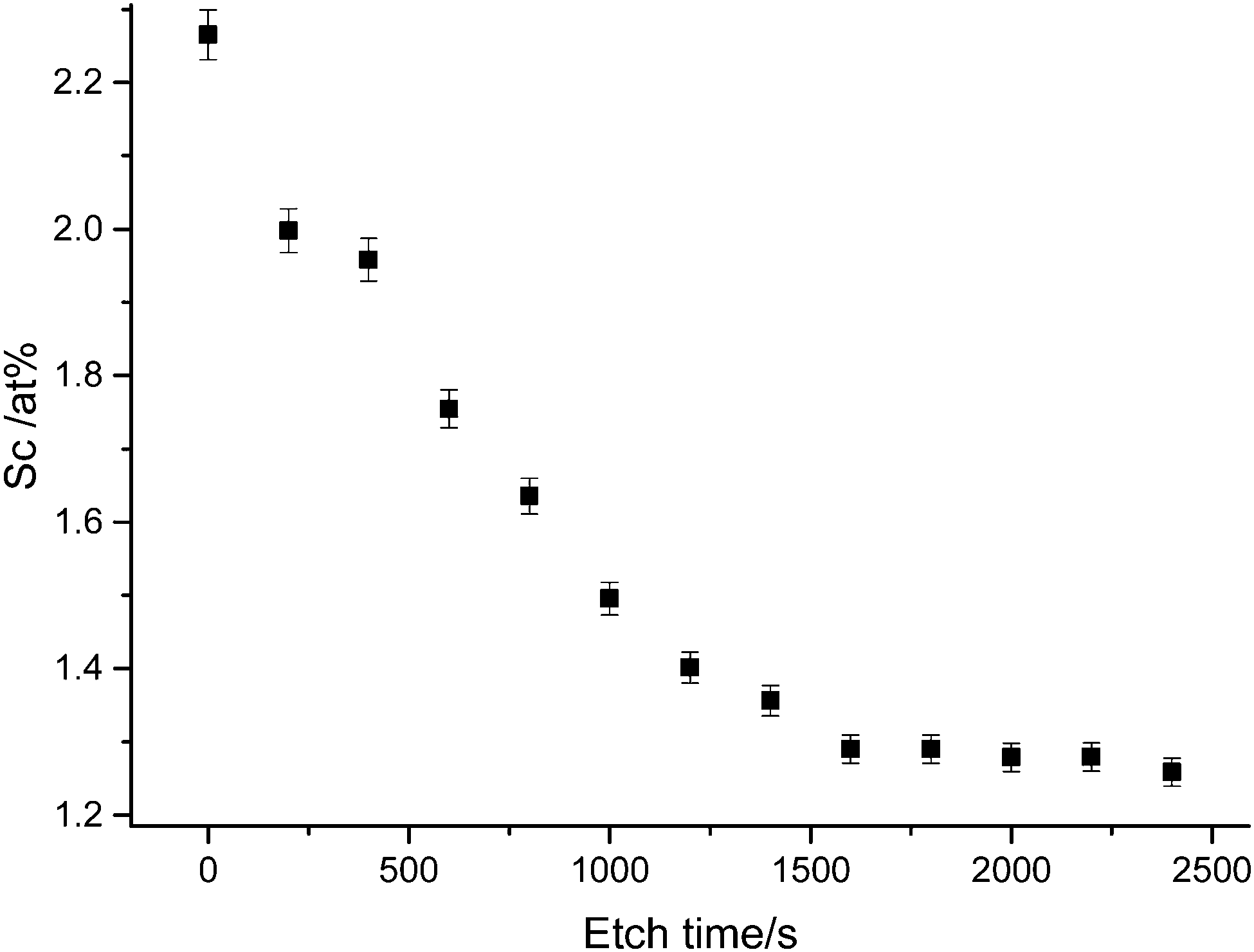 | ||
| Fig. 6 XPS depth profile of ZnO:Sc film illustrating accumulation of Sc(III) species at the film surface. Vertical bars represent the standard deviation of peak area calculations. | ||
X-ray diffraction measurements of the deposited films were made to obtain their crystallographic characteristics. The diffractograms are shown in Fig. 7. The first thing to notice is that all films show a typical hexagonal wurtzite ZnO pattern, with c-axis preferential orientation along the (002) direction.2 There is no apparent secondary crystalline phase, however this does not rule out the presence of small amounts of amorphous Sc2O3 growing at the grain boundaries. There appears in Fig. 7 to be very little shifting of the (002) peak with increased Sc doping, suggestive of a lack of change in the unit cell parameter. This is to be expected, given that the close matching of the crystallographic radii of Sc3+ and Zn2+ (rSc3+ = 0.745 Å and rZn2+ = 0.740 Å) is likely to exert very little expansive strain in the lattice,73 while similar observations have also been made in sol–gel derived ZnO:Sc films in previous study.72 This is supported by the lack of any discernible shift of the E2 phonon mode in the Raman arising from doping (see Fig. S3, ESI†).
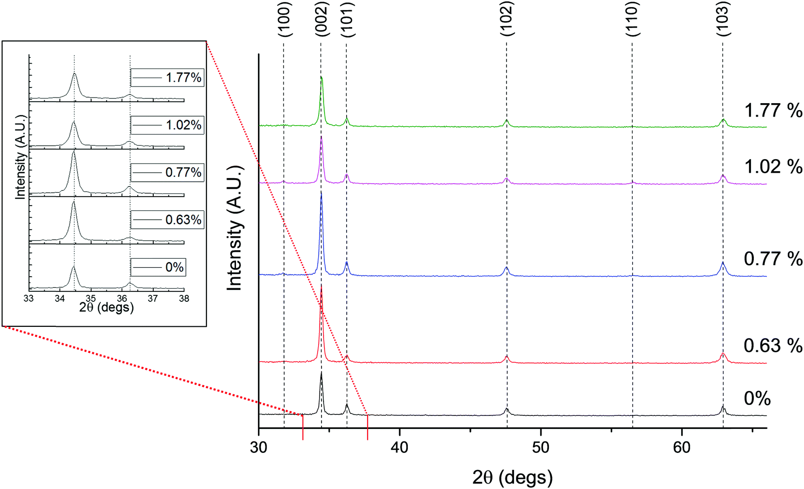 | ||
| Fig. 7 X-ray diffractograms of ZnO:Sc containing varying at% Sc relative to Zn, and (inset) close-up on the shift of the (002) and (101) peaks. | ||
Crystallite sizes were estimated from the width of the (002) peak using Scherrer's formula (see eqn (S1) in ESI†).74 A similar trend was observed in the Scherrer-calculated crystallite diameters with increasing Sc loading as seen in the grain sizes in the microscopy. The estimated crystallite diameters, as shown in Fig. 8, decreased monotonically from around 41 nm for the undoped ZnO to around 34 nm for the film containing 1.77 at% Sc, correlating with a shrink in grain sizes visible from the microscopy (Fig. 9). Crystallite diameters estimated using the Scherrer equation should generally be treated with caution, particularly when the values lie as closely as they do here (i.e. within a 7 nm range); however, we find that the agreement between XRD and microscopy helps to support this observation, as well as the 75% mean agreement of the values in the linear fit (the vertical error in Fig. 8 represents the standard deviation of the data points from a linear fit).
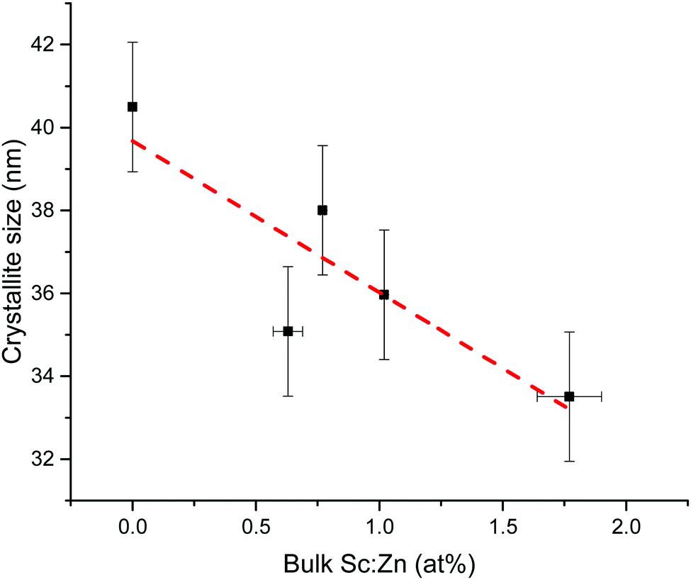 | ||
| Fig. 8 Plot showing effect on crystallite diameter of increased Sc doping in ZnO, as calculated using the Scherrer formula. Sc abundance is expressed relative to Zn in the films. Coefficient of determination R2 = 0.75. | ||
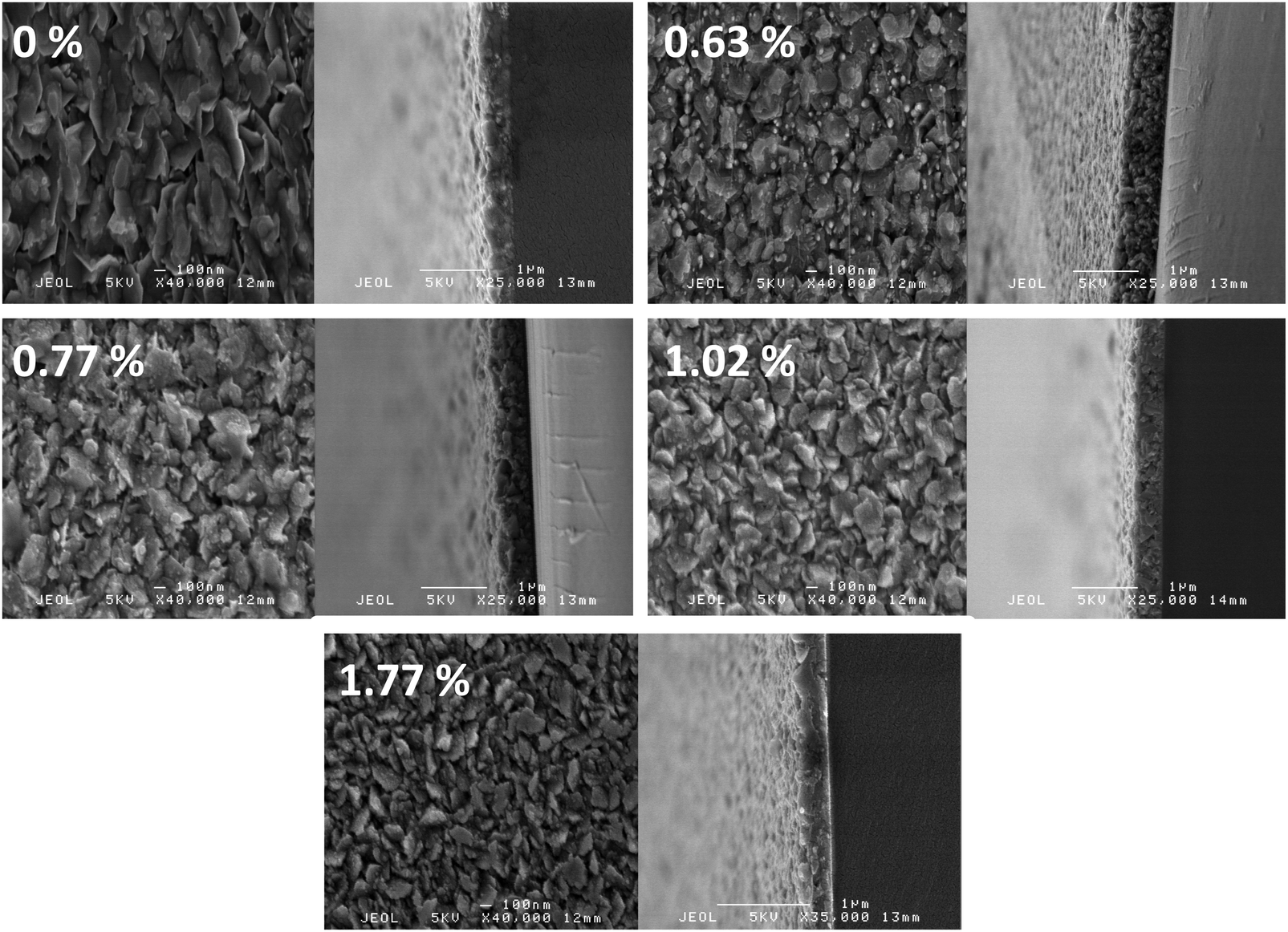 | ||
| Fig. 9 Top-down and side-on scanning electron micrographs of increasingly Sc-doped ZnO samples, expressed in at% relative to Zn. | ||
Lattice parameters for the ZnO:Sc films were calculated using the standard equation for hexagonal lattices (see eqn (S2) in the ESI†). Since peak shift was insignificant in the doped films, there was little significant change in the calculated unit cell parameters, which in the undoped ZnO film were calculated using the (002) and (101) peaks as a = 3.251 Å and c = 5.202 Å. These are in strong agreement with accepted literature experimental values of a = 3.2501 Å and c = 5.2071 Å.75
The texture coefficient (TC(hkl)) for each of the six diffraction peaks in the ZnO:Sc films was calculated from their intensities relative to eachother and to the standard powder pattern (ICSD 29272), as per eqn (S3) in the ESI.† The calculated TC(hkl) are plotted in Fig. S2 in the ESI† against the bulk Sc concentrations in the ZnO:Sc films as obtained by EDX. Although a trend is not clearly apparent for the variation in TC(hkl) with increased doping (as likewise observed by other authors for ZnO:Sc76), there is a clear preference for c-axis orientation as indicated by the consistently strong texture coefficient for the (002) reflection.
Scanning electron microscopy (SEM) of the films, shown in Fig. 9, revealed a clear trend of decreasing grain diameter with increased Sc loading. Thicknesses of the films were measured from the side-on micrographs to be within the range 320–640 nm. From the pure ZnO micrograph it is apparent that the ZnO is growing in a platelet-like morphology, similar to that observed in ZnO:Al films grown via AACVD in previous study.71 As Sc loading increases, this morphology is retained by the ZnO crystallites though there is the distinct appearance of a secondary phase forming at the fringes of the ZnO. As well as having been predicted by our model (see eqn (3)), previous studies suggest that this is probably the amorphous secondary phase Sc2O3, which grows in competition with the doped ZnO:Sc phase.77 The competitive growth of this secondary phase is likely the cause for the reduction in ZnO:Sc grain and crystallite size.
Hall effect measurements were carried out on the films to determine their electrical resistivities and their charge carrier densities and mobilities. It was found that 1.0 at% Sc:Zn in the film was the optimum doping level, exhibiting the lowest resistivity recorded at ρ = 1.2 × 10⁻³ Ω cm, in contrast to ρ = 1.3 × 10⁻¹ Ω cm for the undoped ZnO film, which appears to be the lowest resistivity recorded for a ZnO:Sc film synthesised on glass via a chemical deposition route. The same film exhibited ρ = 2.0 × 10⁻³ Ω cm after having spent 12 months stored under ambient conditions, demonstrating excellent atmospheric stability compared to the infamously unstable Al-doped ZnO.78 The dramatic reduction in resistivity between undoped and Sc-doped ZnO was accompanied by an increase in the carrier density and mobility from n = 2.1 × 1019 cm−3 and μ = 2.3 cm2 V−1 s−1 to n = 7.2 × 1020 cm−3 and μ = 7.5 cm2 V−1 s−1, respectively. Further doping effected a reverse of these properties, such that a slight increase in resistivity and reductions in the charge carrier densities and mobilities were observed (see Fig. 10). A similar pattern was previously observed in ZnO:Sc films deposited via magnetron sputtering.11 This is a common pattern for extrinsic n-type doping of semiconductors. The carrier density pattern is typically attributed to a trade-off between the increasing number of charge carriers being introduced at low dopant levels, with a reduction in carrier density occurring beyond some critical doping point on account of an increasing concentration of compensating vacancy VZn defects arising from their shrinking formation energy accompanied by a rising formation energy for ScZn, as supported by our calculations (see Fig. 3) and previous work.32 In the case of mobility, the reduction occurs at higher doping levels due to an increase in the probability of propagating electrons being scattered at dopant sites and a shrinking crystallite size. The cause for the initial increase in mobility is unclear, though previous ZnO:Al doping study has noted an increase in the carrier mean free path at low dopant levels, in spite of a shrinking crystallite diameter relative to the undoped material.79 The ionised impurity scattering is typically the dominant scattering mechanism at higher dopant levels (n = 1020–1021 cm−3), though grain boundary scattering becomes more significant at low dopant levels (n = 1019–1020 cm−3).80 ZnO films grown previously via AACVD have yielded closely comparable mobilities (μ = 9.7 cm2 V−1 s−1 in ZnO:Al, F).71
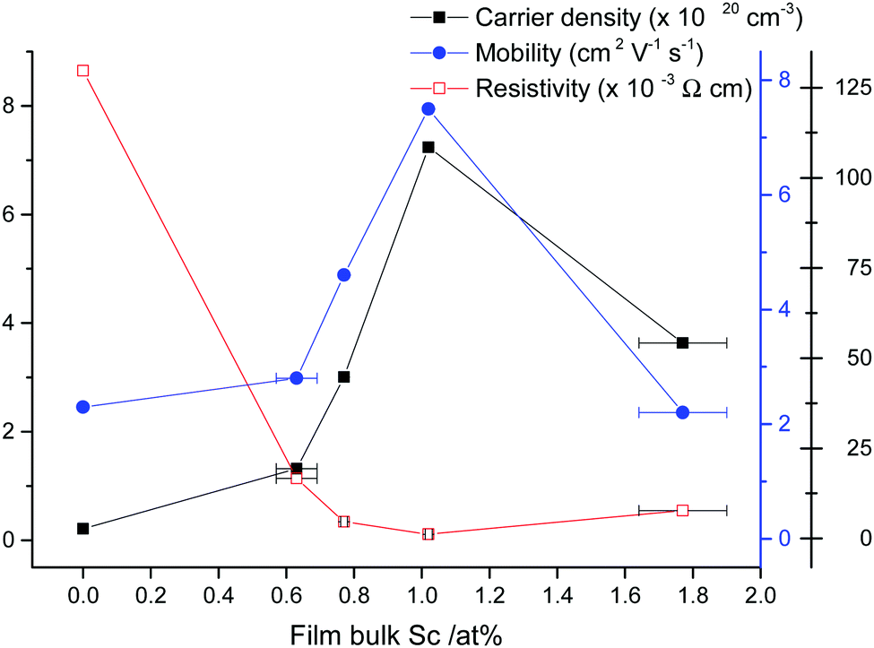 | ||
| Fig. 10 Electrical properties for SZO films as obtained by Hall effect measurements. | ||
It is also interesting to note that those nominally undoped ZnO films, deposited also via AACVD but from a diethyl zinc precursor as opposed to the zinc acetate precursor used here, exhibit low resistivities similar to those measured for Al-doped ZnO in the same study (ρZnO ≈ ρZnO:Al = 2.2 × 10⁻³ Ω cm),71 while undoped ZnO deposited here from zinc acetate has ρ = 1.3 × 10⁻¹ Ω cm. It is often argued that conductivity in nominally undoped ZnO originates from nonstoichiometry which gives rise to electron-donating oxygen vacancies VO and interstitial Znint in the ZnO.1,32 However, since our calculations (and others’30) suggest that VO is a relatively deep donor (see Section 3.1) while Znint has been shown to have a relatively high formation energy,30 we consider that this effect is due to a difference in the degree of hydrogen doping of the ZnO by interstitial Hint, a shallow donor which should therefore be the dominant donor defect in these films.30,65,66 First-principles work by Oba et al.30 suggests that such defects are likewise preferentially formed under an oxygen-poor deposition environment, which helps to rationalise the trend that lower resistivities are observed in nominally undoped ZnO films deposited from the oxygen-poor diethyl zinc precursor ([Zn(CH2CH3)2]),71 when compared with those obtained from the zinc acetate precursor ([Zn(OCOCH3)2]), which is richer in oxygen, in the present work. It should be noted that overall, we consider the deposition environment used in the present study to be largely oxygen-poor, having been carried out under inert gas with the only sources of oxygen for oxide formation being the molecular acetate precursors and in the solvents present.
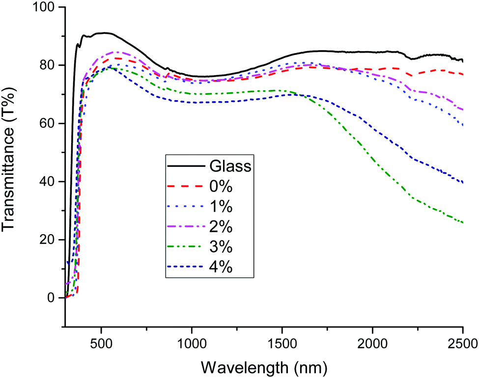
UV-visible transmission measurements of the doped ZnO:Sc samples are plotted in Fig. 11. The films were visibly transparent and uncoloured. It is evident that an increased level of doping leads to a reduction in the transmittance of the films in the infrared, resulting in a minimum transmittance occurring in the near-infrared at 2500 nm in the ZnO:Sc film with the highest charge carrier density. This is a commonly observed phenomenon in n-type TCOs and is related to an increasing low-energy surface plasmon resonance (SPR) effect at high carrier densities, where increased charge carrier density is directly correlated with increased infrared reflectivity.5 A further increase in Sc doping beyond the optimum level in the ZnO:Sc was observed in the Hall measurements to effect a reduction in the charge carrier density, which (as expected) is directly observed to reduce the infrared reflectivity. There is a high degree of transmission in the visible range (400–750 nm) in all films, with 88% visible transmission in the most electrically conductive sample and the highest visible transmission occurring in pure ZnO at 91%. The doping has the effect of marginally reducing the visible transmission, as expected according to the principle of free carrier absorption (FCA).6
 | ||
| Fig. 11 UV-visible transmission spectra of plain glass and increasingly Sc-doped ZnO films. | ||
Optical band gaps of thin film TCOs are often estimated using the Tauc method, in which a plot is constructed from optical absorption data near to the absorption edge of the material (here appearing around 380 nm). Where α is the optical absorption coefficient, h is Planck's constant and ν is the incident photon frequency, for a direct band gap material such as ZnO a plot of (αhν)2vs. hν is drawn, such that the steepest gradient occurring along the absorption edge is linearly extrapolated to the x-intercept to find the film's optical band gap Eoptg.81 However, it is generally found that band gaps estimated using the Tauc method for degenerate polycrystalline semiconductors are underestimated when compared with band gaps found using other methods such as spectroscopic ellipsometry (SE). For instance, applying the uncorrected Tauc method here yields a band gap of Eoptg = 3.28 eV for nominally undoped ZnO, which agrees with numerous previous experimental Tauc band gaps for undoped ZnO of Eoptg = 3.27 ± 0.02 eV.76,82,83 However, SE data suggests that ZnO thin films should have a band gap of Eoptg = 3.37 eV.84 In a recent discussion on this dilemma, Dolgonos et al. suggest that the issue arises from the fact that the Tauc method was originally developed for estimation of the band gap of amorphous Ge, a nondegenerate semiconductor.85 Aside from the fact that assumptions regarding localisation of energy states in an amorphous material might not necessarily hold for a polycrystalline material (which instead contains far greater long-range order), accurate extraction of Eg information from absorption data is further complicated by broadening of initial and final electron–hole pair states upon photon absorption arising from time-dependent perturbation theory effects. Dolgonos et al. argue that a broadening term Γ for this effect can be estimated from optical absorption data, such that the separation of the x-intercepts of tangents drawn from α and α2 curves gives  , which can be added to the Tauc-estimated band gap to give a more accurate, corrected estimate for the band gap.85 This correction was carried out on absorption data in the present work, in order to obtain more accurate band gap estimates for degenerate ZnO:Sc (see Fig. 12). Assuming a linear relationship between increased Sc content and optical band gap (coefficient of determination R2 = 0.81),86 at 0% Sc doping (i.e. for pure ZnO) this correction yields Eoptg = 3.34 ± 0.03 eV, while the most electrically conductive ZnO:Sc sample at 1.02 at% bulk Sc:Zn has Eoptg = 3.45 ± 0.03 eV (see Fig. 13). Such an observation would be consistent with the Moss-Burstein band-gap widening principle which attributes this effect to an increasing occupation of the lowest states of the CB with increased doping.6 The same trend has been observed previously for ZnO:Sc thin films.4 These estimates are significantly closer to the experimental values obtained from SE (3.37 eV for ZnO),30 while we acknowledge that error in the corrected Tauc method is still inherent due to the necessary extrapolation step. Aside from this, variation in calculated ZnO band gaps arises between studies from effects such as varying degrees of crystallinity and degeneracy in nominally undoped ZnO films due to intrinsic n-type doping.
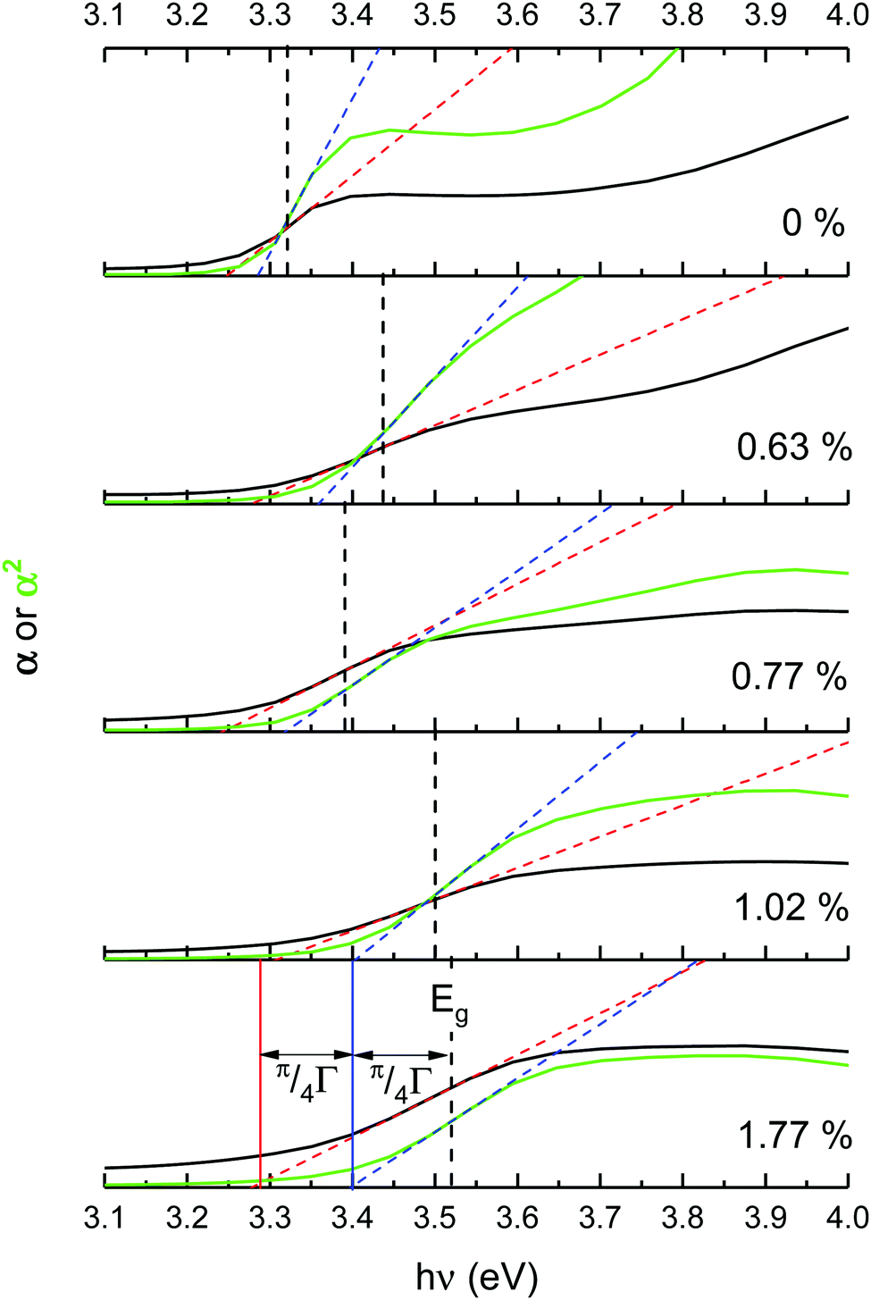 | ||
| Fig. 12 Corrected Tauc optical band gap plots calculated from UV/vis transmission spectra at the absorption edge, for Sc-doped ZnO films containing increasing amounts of bulk Sc (expressed relative to Zn in at%). | ||
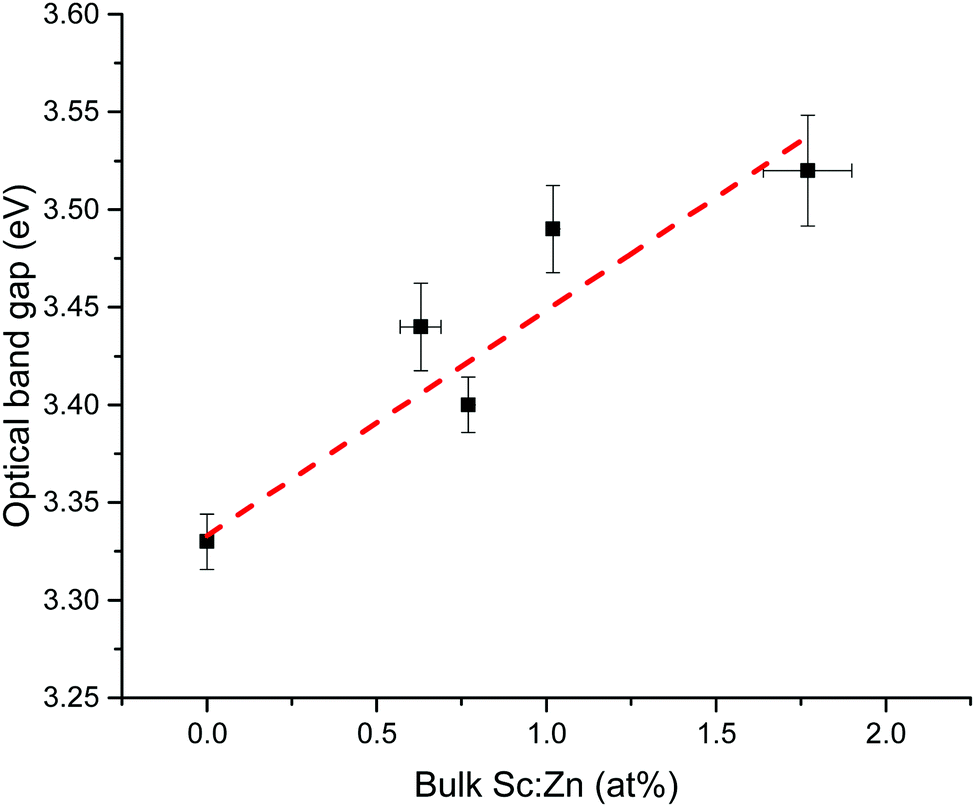 | ||
| Fig. 13 Linear trend in corrected Tauc optical band gap vs. amount of bulk Sc (expressed relative to Zn in at%). | ||
4. Conclusions
A computational model for Sc doping of ZnO has been constructed using hybrid density functional theory calculations alongside a synthetic experimental study of ZnO:Sc thin films. Strong correlation between the theoretical and experimental results has offered an insight into the defect landscape of Sc-doped ZnO and helped to rationalise the trends observed in the Hall effect measurements, while showing that substitutional Sc (ScZn) acts as a shallow donor in ZnO and indicating that oxygen-poor deposition conditions are necessary for achieving efficient n-type doping. Transparent and n-type conducting Sc-doped ZnO thin films were successfully deposited via a one-pot aerosol-assisted chemical vapour deposition onto silica barrier glass substrates. It can therefore be concluded that the deposition under nitrogen from acetates of Zn(II) and Sc(III) provides sufficiently O-poor growth conditions for efficient ScZn donor doping. Future experimental work might seek to explore the ZnO:Sc growth environment further by tweaking the balance of Zn and O abundance during film growth. A range of films containing various Sc quantities were synthesised in order to demonstrate growth behaviours and optimal deposition conditions. All syntheses were carried out in a single-step deposition from an alcoholic solution of the organometallic salt precursors, using a range of Sc:Zn precursor ratios between 0.0 and 4.0 mol%. Optimal electrical properties were obtained in the film containing 1.0 at% bulk Sc relative to Zn; this film exhibited the lowest resistivity at ρ = 1.2 × 10⁻³ Ω cm, in contrast to ρ = 1.3 × 10⁻¹ Ω cm for the undoped ZnO film. This appears to be the lowest resistivity recorded for a ZnO:Sc film on glass via a chemical deposition route, and indeed the only reported instance of electrically conductive ZnO:Sc having been deposited via chemical vapour deposition. That same film also had carrier density n = 7.2 × 1020 cm−3 and electron mobility μ = 7.5 cm2 V−1 s−1, and was highly transparent in the visible with 88% transmission (400–750 nm). Storage of the sample for 12 months under ambient conditions effected only a slight increase of resistivity, to ρ = 2.0 × 10⁻³ Ω cm, suggesting excellent atmospheric stability. Increased Sc doping led to reduced ZnO grain and crystallite sizes and widened band gaps, with Eoptg = 3.45 ± 0.03 eV in the most conductive sample and Eoptg = 3.34 ± 0.03 eV in nominally undoped ZnO, as estimated using a corrected Tauc method. No observable shift in unit cell dimensions occurred with doping, as attributed to the close matching of the Sc(III) and Zn(II) ionic radii. In summary, in spite of having thus far received relatively little attention in the materials research community, Sc-doped ZnO has been shown to be a highly promising transparent conducting oxide warranting further investigation, for which it is hoped that this paper will serve as a useful reference.Acknowledgements
Thanks are due to Dr Chris Blackman, Dr Steve Firth and Sultan Ben Jaber for assistance with Raman spectroscopy. The authors would also like to acknowledge and thank NSG Pilkington Glass Ltd. and the EPSRC for studentship funding (S. C. D.) through the M3S Doctoral Training Centre (grant EP/G036675) and also for grant EP/N01572X/1. This work made use of the ARCHER UK National Supercomputing Service (http://www.archer.ac.uk) via our membership of the UK's HEC Materials Chemistry Consortium, which is also funded by the EPSRC (EP/L000202). The UCL Legion and Grace HPC Facilities (Legion@UCL and Grace@UCL) were also used in the completion of this work.References
- R. Pandey, S. Yuldashev, H. D. Nguyen, H. C. Jeon and T. W. Kang, Curr. Appl. Phys., 2012, 12, S56–S58 CrossRef.
- R. S. Ajimsha, A. K. Das, P. Misra, M. P. Joshi, L. M. Kukreja, R. Kumar, T. K. Sharma and S. M. Oak, J. Alloys Compd., 2015, 638, 55–58 CrossRef CAS.
- H. M. Yates, J. M. Gaskell, M. E. Thomson, D. W. Sheel, B. Delaup and M. Morales-Masis, Thin Solid Films, 2015, 590, 260–265 CrossRef CAS.
- R. Sharma, K. Sehrawat and R. M. Mehra, Curr. Appl. Phys., 2010, 10, 164–170 CrossRef.
- N. Noor, C. K. T. Chew, D. S. Bhachu, M. R. Waugh, C. J. Carmalt and I. P. Parkin, J. Mater. Chem. C, 2015, 3, 9359–9368 RSC.
- S. C. Dixon, D. O. Scanlon, C. J. Carmalt and I. P. Parkin, J. Mater. Chem. C, 2016, 419, 462–465 Search PubMed.
- U. Betz, M. Kharrazi Olsson, J. Marthy, M. F. Escolá and F. Atamny, Surf. Coat. Technol., 2006, 200, 5751–5759 CrossRef CAS.
- European Commission, Report on critical raw materials for the EU, Report of the Ad hoc Working Group on defining critical raw materials, 2014.
- G. Hautier, A. Miglio, D. Waroquiers, G.-M. Rignanese and X. Gonze, Chem. Mater., 2014, 26, 5447–5458 CrossRef CAS.
- D. S. Bhachu, D. O. Scanlon, G. Sankar, T. D. Veal, R. G. Egdell, G. Cibin, A. J. Dent, C. E. Knapp, C. J. Carmalt and I. P. Parkin, Chem. Mater., 2015, 27, 2788–2796 CrossRef CAS.
- T. Minami, T. Yamamoto and T. Miyata, Thin Solid Films, 2000, 366, 63–68 CrossRef CAS.
- P. Marchand, I. A. Hassan, I. P. Parkin and C. J. Carmalt, Dalton Trans., 2013, 42, 9406 RSC.
- S. C. Dixon, W. J. Peveler, N. Noor, J. C. Bear and I. P. Parkin, RSC Adv., 2016, 6, 31146–31152 RSC.
- M. G. Nolan, J. A. Hamilton, S. O’Brien, G. Bruno, L. Pereira, E. Fortunato, R. Martins, I. M. Povey and M. E. Pemble, J. Photochem. Photobiol., A, 2011, 219, 10–15 CrossRef CAS.
- G. Kresse and J. Hafner, Phys. Rev. B: Condens. Matter Mater. Phys., 1993, 47, 558–561 CrossRef CAS.
- G. Kresse and J. Hafner, Phys. Rev. B: Condens. Matter Mater. Phys., 1994, 49, 14251–14269 CrossRef CAS.
- G. Kresse, J. Furthmu, J. Furthmüller, G. Kresse and J. Furthmu, Phys. Rev. B: Condens. Matter Mater. Phys., 1996, 54, 11169 CrossRef CAS.
- G. Kresse and J. Furthmüller, Comput. Mater. Sci., 1996, 6, 15–50 CrossRef CAS.
- P. E. Blochl, Phys. Rev. B: Condens. Matter Mater. Phys., 1994, 50, 17953–17979 CrossRef.
- J. Heyd, G. E. Scuseria and M. Ernzerhof, J. Chem. Phys., 2003, 118, 8207–8215 CrossRef CAS.
- D. O. Scanlon and G. W. Watson, J. Mater. Chem., 2012, 22, 25236 RSC.
- A. M. Ganose and D. O. Scanlon, J. Mater. Chem. C, 2016, 4, 1467–1475 RSC.
- J. Buckeridge, K. T. Butler, C. R. A. Catlow, A. J. Logsdail, D. O. Scanlon, S. A. Shevlin, S. M. Woodley, A. A. Sokol and A. Walsh, Chem. Mater., 2015, 27, 3844–3851 CrossRef CAS.
- B. A. D. Williamson, J. Buckeridge, J. Brown, S. Ansbro, R. G. Palgrave and D. O. Scanlon, Chem. Mater., 2017, 29, 2402–2413 CrossRef CAS.
- D. O. Scanlon, A. Regoutz, R. G. Egdell, D. J. Morgan and G. W. Watson, Appl. Phys. Lett., 2013, 103, 262108 CrossRef.
- D. S. Bhachu, S. Sathasivam, G. Sankar, D. O. Scanlon, G. Cibin, C. J. Carmalt, I. P. Parkin, G. W. Watson, S. M. Bawaked, A. Y. Obaid, S. Al-Thabaiti and S. N. Basahel, Adv. Funct. Mater., 2014, 24, 5075–5085 CrossRef CAS.
- D. O. Scanlon, J. Buckeridge, C. R. A. Catlow and G. W. Watson, J. Mater. Chem. C, 2014, 2, 3429 RSC.
- D. O. Scanlon and G. W. Watson, Chem. Mater., 2009, 21, 5435–5442 CrossRef CAS.
- D. O. Scanlon, C. W. Dunnill, J. Buckeridge, S. A. Shevlin, A. J. Logsdail, S. M. Woodley, C. R. A. Catlow, M. J. Powell, R. G. Palgrave, I. P. Parkin, G. W. Watson, T. W. Keal, P. Sherwood, A. Walsh and A. A. Sokol, Nat. Mater., 2013, 12, 798–801 CrossRef CAS PubMed.
- F. Oba, A. Togo, I. Tanaka, J. Paier and G. Kresse, Phys. Rev. B: Condens. Matter Mater. Phys., 2008, 77, 245202 CrossRef.
- A. Walsh, J. L. F. Da Silva, Y. Yan, M. M. Al-Jassim and S. Wei, Phys. Rev. B: Condens. Matter Mater. Phys., 2009, 79, 73105 CrossRef.
- S. Lany and A. Zunger, Phys. Rev. Lett., 2007, 98, 45501 CrossRef PubMed.
- A. Janotti, J. B. Varley, P. Rinke, N. Umezawa, G. Kresse and C. G. Van De Walle, Phys. Rev. B: Condens. Matter Mater. Phys., 2010, 81, 85212 CrossRef.
- J. L. Lyons, A. Janotti and C. G. Van De Walle, J. Appl. Phys., 2014, 115, 12014 CrossRef.
- P. Deák, B. Aradi and T. Frauenheim, Phys. Rev. B: Condens. Matter Mater. Phys., 2011, 83, 1–7 CrossRef.
- J. B. Varley, A. Janotti and C. G. Van De Walle, Adv. Mater., 2011, 23, 2343–2347 CrossRef CAS PubMed.
- H. Chen and J. A. Dawson, J. Phys. Chem. C, 2015, 119, 15890–15895 CAS.
- H. A. Huy, B. Aradi, T. Frauenheim and P. Deák, Phys. Rev. B: Condens. Matter Mater. Phys., 2011, 83, 1–7 CrossRef.
- F. Oba, M. Choi, A. Togo, A. Seko and I. Tanaka, J. Phys.: Condens. Matter, 2010, 22, 384211 CrossRef PubMed.
- S. J. Clark, J. Robertson, S. Lany and A. Zunger, Phys. Rev. B: Condens. Matter Mater. Phys., 2010, 81, 1–5 CrossRef.
- D. O. Scanlon, Phys. Rev. B: Condens. Matter Mater. Phys., 2013, 87, 161201 CrossRef.
- S. Lany and A. Zunger, Phys. Rev. B: Condens. Matter Mater. Phys., 2008, 78, 17–20 Search PubMed.
- H. Peng, D. O. Scanlon, V. Stevanovic, J. Vidal, G. W. Watson and S. Lany, Phys. Rev. B: Condens. Matter Mater. Phys., 2013, 88, 1–7 Search PubMed.
- P. A. Schultz, Phys. Rev. Lett., 2006, 96, 246401 CrossRef PubMed.
- D. C. Reynolds, D. C. Look, B. Jogai, C. W. Litton, G. Cantwell and W. C. Harsch, Phys. Rev. B: Condens. Matter Mater. Phys., 1999, 60, 2340–2344 CrossRef CAS.
- H. Karzel, W. Potzel, M. Köfferlein, W. Schiessl, M. Steiner, U. Hiller, G. M. Kalvius, D. W. Mitchell, T. P. Das, P. Blaha, K. Schwarz and M. P. Pasternak, Phys. Rev. B: Condens. Matter Mater. Phys., 1996, 53, 11425–11438 CrossRef CAS.
- S. Desgreniers, Phys. Rev. B: Condens. Matter Mater. Phys., 1998, 58, 14102–14105 CrossRef CAS.
- R. R. Reeber, J. Appl. Phys., 1970, 41, 5063–5066 CrossRef CAS.
- A. Janotti and C. G. Van De Walle, Phys. Rev. B: Condens. Matter Mater. Phys., 2007, 76, 1–22 CrossRef.
- C. G. Van De Walle and J. Neugebauer, J. Appl. Phys., 2004, 95, 3851–3879 CrossRef CAS.
- N. D. M. Hine, K. Frensch, W. M. C. Foulkes and M. W. Finnis, Phys. Rev. B: Condens. Matter Mater. Phys., 2009, 79, 24112 CrossRef.
- R. M. Nieminen, Modell. Simul. Mater. Sci. Eng., 2009, 17, 84001 CrossRef.
- S. T. Murphy and N. D. M. Hine, Phys. Rev. B: Condens. Matter Mater. Phys., 2013, 87, 1–18 Search PubMed.
- C. Freysoldt, J. Neugebauer and C. G. Van De Walle, Phys. Rev. Lett., 2009, 102, 1–4 CrossRef PubMed.
- M. Lorenz, C. Schmidt, G. Benndorf, T. Böntgen, H. Hochmuth, R. Böttcher, A. Pöppl, D. Spemann and M. Grundmann, J. Phys. D: Appl. Phys., 2013, 46, 65311 CrossRef.
- O. Mryasov and A. Freeman, Phys. Rev. B: Condens. Matter Mater. Phys., 2001, 64, 2–4 CrossRef.
- S. K. Vasheghani Farahani, T. D. Veal, J. J. Mudd, D. O. Scanlon, G. W. Watson, O. Bierwagen, M. E. White, J. S. Speck and C. F. McConville, Phys. Rev. B: Condens. Matter Mater. Phys., 2014, 90, 1–9 CrossRef.
- K. J. Button, D. R. Cohn, M. Von Ortenbert, B. Lax, E. Mollwo and R. Helbig, Phys. Rev. Lett., 1972, 28, 1637–1639 CrossRef CAS.
- F. Oba, S. R. Nishitani, S. Isotani, H. Adachi and I. Tanaka, J. Appl. Phys., 2001, 90, 824 CrossRef CAS.
- A. Janotti and C. G. Van De Walle, J. Cryst. Growth, 2006, 287, 58–65 CrossRef CAS.
- S. B. Zhang, S.-H. Wei and A. Zunger, Phys. Rev. B: Condens. Matter Mater. Phys., 2001, 63, 75205 CrossRef.
- X. J. Wang, L. S. Vlasenko, S. J. Pearton, W. M. Chen and I. A. Buyanova, J. Phys. D: Appl. Phys., 2009, 42, 175411 CrossRef.
- D. M. Hofmann, D. Pfisterer, J. Sann, B. K. Meyer, R. Tena-Zaera, V. Munoz-Sanjose, T. Frank and G. Pensl, Appl. Phys. A: Mater. Sci. Process., 2007, 88, 147–151 CrossRef CAS.
- L. S. Vlasenko, Appl. Magn. Reson., 2010, 39, 103–111 CrossRef CAS.
- C. G. Van de Walle, Phys. Rev. Lett., 2000, 85, 1012–1015 CrossRef CAS PubMed.
- S. F. J. Cox, E. A. Davis, S. P. Cottrell, P. J. C. King, J. S. Lord, J. M. Gil, H. V. Alberto, R. C. Vilão, J. Piroto Duarte, N. Ayres de Campos, A. Weidinger, R. L. Lichti and S. J. C. Irvine, Phys. Rev. Lett., 2001, 86, 2601–2604 CrossRef CAS PubMed.
- S. Lany and A. Zunger, Phys. Rev. B: Condens. Matter Mater. Phys., 2009, 80, 1–5 CrossRef.
- K. C. Patil, G. V. Chandrashekhar, M. V. George and C. N. R. Rao, Can. J. Chem., 1968, 46, 257–265 CrossRef CAS.
- M. Yoshio and S. Shunsuke, J. Inorg. Nucl. Chem., 1980, 42, 299–301 CrossRef.
- Y. Yang, H. Chen, B. Zhao and X. Bao, J. Cryst. Growth, 2004, 263, 447–453 CrossRef CAS.
- S. D. Ponja, S. Sathasivam, I. P. Parkin and C. J. Carmalt, RSC Adv., 2014, 4, 49723–49728 RSC.
- J. Chen, D. Chen, J. He, S. Zhang and Z. Chen, Appl. Surf. Sci., 2009, 255, 9413–9419 CrossRef CAS.
- K.-C. Peng, J.-C. Lin, C. A. Tseng and S.-L. Lee, Surf. Coat. Technol., 2008, 202, 5425–5430 CrossRef CAS.
- A. L. Patterson, Phys. Rev., 1939, 56, 978–982 CrossRef CAS.
- E. H. Kisi and M. M. Elcombe, Acta Crystallogr., Sect. C: Cryst. Struct. Commun., 1989, 45, 1867–1870 CrossRef.
- A. Yumak, G. Turgut, O. Kamoun, H. Ozisik, E. Deligoz, P. Petkova, R. Mimouni, K. Boubaker, M. Amlouk and S. Goumri-Said, Mater. Sci. Semicond. Process., 2015, 39, 103–111 CrossRef CAS.
- J.-C. Lin, K.-C. Peng, H.-L. Liao and S.-L. Lee, Thin Solid Films, 2008, 516, 5349–5354 CrossRef CAS.
- C. Zhu, J. Li, Y. Yang, X. Zhao, W. Zou, R. Tan and W. Song, Thin Solid Films, 2017, 634, 155–159 CrossRef CAS.
- R. Bel Hadj Tahar, J. Eur. Ceram. Soc., 2005, 25, 3301–3306 CrossRef.
- T. Minami, H. Sato, K. Ohashi, T. Tomofuji and S. Takata, J. Cryst. Growth, 1992, 117, 370–374 CrossRef CAS.
- J. Tauc, R. Grigorovici and A. Vancu, Phys. Status Solidi, 1966, 15, 627–637 CrossRef CAS.
- S.-S. Lin, J.-L. Huang and P. Šajgalik, Surf. Coat. Technol., 2005, 191, 286–292 CrossRef CAS.
- A. Jain, P. Sagar and R. M. Mehra, Solid-State Electron., 2006, 50, 1420–1424 CrossRef CAS.
- P. L. Washington, H. C. Ong, J. Y. Dai and R. P. H. Chang, Appl. Phys. Lett., 1998, 72, 3261–3263 CrossRef CAS.
- A. Dolgonos, T. O. Mason and K. R. Poeppelmeier, J. Solid State Chem., 2016, 240, 43–48 CrossRef CAS.
- J. Sans, J. Sánchez-Royo, A. Segura, G. Tobias and E. Canadell, Phys. Rev. B: Condens. Matter Mater. Phys., 2009, 79, 1–9 CrossRef.
Footnote |
| † Electronic supplementary information (ESI) available. See DOI: 10.1039/c7tc02389h |
| This journal is © The Royal Society of Chemistry 2017 |