
 Open Access Article
 This Open Access Article is licensed under a
 Creative Commons Attribution 3.0 Unported Licence
Band gap evolution and a piezoelectric-to-electrostrictive crossover in (1 − x)KNbO3–x(Ba0.5Bi0.5)(Nb0.5Zn0.5)O3 ceramics†
Cristina
Pascual-Gonzalez
a,
Giorgio
Schileo
b,
Amir
Khesro
b,
Iasmi
Sterianou
a,
Dawei
Wang
b,
Ian M.
Reaney
b and
Antonio
Feteira
 *a
*a
aChristian Doppler Lab on Advanced Ferroic Oxides, Materials and Engineering Research Institute, Sheffield Hallam University, Howard Street, S1 1WB, Sheffield, UK. E-mail: a.feteira@shu.ac.uk
bDepartment of Materials Engineering and Science, The University of Sheffield, S1 4JD, Sheffield, UK
First published on 24th January 2017
Abstract
The band gap of (1 − x)KNbO3–x(Ba0.5Bi0.5)(Nb0.5Zn0.5)O3 (0 ≤ x ≤ 0.25) ceramics narrows slightly from 3.22 eV for x = 0 to 2.89 eV for x = 0.25, in broad agreement with first-principles calculations [Phys. Rev. B, 2014, 89, 235105]. In addition, an unreported piezoelectric-to-electrostrictive crossover is observed in this compositional range, which is accompanied by a continuous decrease of the maximum electric field-induced strain due to the presence of a non-ferroelectric phase. An electrostriction coefficient of 0.023 m4 C−2 is measured for x = 0.05, whilst no electromechanical response is observed for non-ferroelectric x = 0.25, even under an applied electric field of 80 kV cm−1.
Introduction
Coupling of light absorption in ferroelectrics with properties such as photovoltage, photostriction and photocatalysis has been envisaged as a route to create novel photoactive devices.1–8 Spontaneous polarization in ferroelectrics offers an internal electric field to effectively separate photogenerated charge carriers, enabling them not only to reach the surface by interacting and reacting with molecules in the surrounding media but also to create photo-induced currents.9 Solar energy harvesting using ferroelectrics such as KNbO3 (KN) has been recently proposed as a potential route for sustainable, non-hazardous, and economically viable technologies to reduce our reliance on fossil fuels.10KN is a prototypical ferroelectric (FE) perovskite. In the classic work reported by Shirane et al.,11 the room-temperature spontaneous polarisation of single-domain KN was reported as 41 ± 2 μC cm−2. This large spontaneous polarisation was rationalised on the basis of the non-centrosymmetric position of Nb5+ cations within the NbO6 octahedra. This distortion is driven by the hybridisation of the empty d-orbitals of Nb5+ with the O2− p-orbitals. Upon cooling from high temperature, KN undergoes a series of structural phase transitions. A paraelectric-to-ferroelectric phase transition occurs at 410 °C when the crystal symmetry of KN changes from cubic centrosymmetric (Pm![[3 with combining macron]](https://www.rsc.org/images/entities/char_0033_0304.gif) m) to tetragonal non-centrosymmetric (P4mm). Two ferroelectric-to-ferroelectric phase transitions occur upon further cooling. At 220 °C the crystal symmetry changes from tetragonal (P4mm) to orthorhombic (Amm2) and at −55 °C it changes from orthorhombic (Amm2) to rhombohedral (R3m). These phase transitions are accompanied by anomalies in the temperature dependence of the relative permittivity, εr, of KN. The single-crystal KN exhibits a maximum εr of ∼4000 at the Curie temperature of 410 °C, whereas at room temperature it is ∼1000. In ceramics, the room-temperature εr was reported to vary between ∼300 and 800.12–15 This wide range of εr values is linked to several aspects of the final microstructures, such as variations in density, texture and grain size. The fabrication of KN ceramics is difficult with problems mainly associated with unsuccessful densification due to its low melting temperature (<1100 °C). In addition, the structural stability of KN ceramics encompassing residual K4Nb6O17 is dramatically affected by moisture. To minimise the detrimental effects of moisture, several authors studied the impact of processing conditions13,16,17 on KN and the prescribed remedial procedures.14,15 For example, Matsumoto et al.18 demonstrated that through careful processing, including the addition of 1.2 wt% of MnCO3 to reduce electrical conductivity and enhance densification, it is possible to prepare KN ceramics by the conventional solid-state reaction route that show a respectable 0.22% electric-field induced strain under a unipolar field of 80 kV cm−1. More recently, Lv et al.19 demonstrated the addition of ZnO to KN to simultaneously improve both the electrical properties and the resistance to moisture.
m) to tetragonal non-centrosymmetric (P4mm). Two ferroelectric-to-ferroelectric phase transitions occur upon further cooling. At 220 °C the crystal symmetry changes from tetragonal (P4mm) to orthorhombic (Amm2) and at −55 °C it changes from orthorhombic (Amm2) to rhombohedral (R3m). These phase transitions are accompanied by anomalies in the temperature dependence of the relative permittivity, εr, of KN. The single-crystal KN exhibits a maximum εr of ∼4000 at the Curie temperature of 410 °C, whereas at room temperature it is ∼1000. In ceramics, the room-temperature εr was reported to vary between ∼300 and 800.12–15 This wide range of εr values is linked to several aspects of the final microstructures, such as variations in density, texture and grain size. The fabrication of KN ceramics is difficult with problems mainly associated with unsuccessful densification due to its low melting temperature (<1100 °C). In addition, the structural stability of KN ceramics encompassing residual K4Nb6O17 is dramatically affected by moisture. To minimise the detrimental effects of moisture, several authors studied the impact of processing conditions13,16,17 on KN and the prescribed remedial procedures.14,15 For example, Matsumoto et al.18 demonstrated that through careful processing, including the addition of 1.2 wt% of MnCO3 to reduce electrical conductivity and enhance densification, it is possible to prepare KN ceramics by the conventional solid-state reaction route that show a respectable 0.22% electric-field induced strain under a unipolar field of 80 kV cm−1. More recently, Lv et al.19 demonstrated the addition of ZnO to KN to simultaneously improve both the electrical properties and the resistance to moisture.
Interest in KN has been renewed by a recent proposal on its potential as a base material for both nanogenerators20–22 and photovoltaic applications.10,23,24 Grinberg et al.10 reported the preparation of (1 − x)KNbO3–xBaNi0.5Nb0.5O3−δ (KBNNO) ceramics which exhibit high polarization (40 μC cm−2) and band gaps as low as 1.1 eV. The combination of a low band gap and high polarization is achieved through ferroelectrically active Nb5+ combined with Ni2+ and O vacancies. However, this new ferroelectric oxide relies on the presence of a large concentration of oxygen vacancies, detrimental to polarization switching, which can also trap photogenerated carriers and increase the charge recombination rate. According to first-principles calculations, KN doped with Zn2+ for Nb5+, charge compensated at A-sites with different combinations of higher valence cations, is a semiconducting ferroelectric with high spontaneous polarization. First-principles calculations for 0.75KNbO3–0.25(Ba0.5Bi0.5)(Nb0.5Zn0.5)O3 gave a value of ∼37 μC cm−2, which is typical for a robust ferroelectric material.25 Moreover, it was also calculated that the band gap drops from 3.15 eV for orthorhombic KNbO3 to 2.90 eV for 0.75KNbO3–0.25(Ba0.5Bi0.5)(Nb0.5Zn0.5)O3. It was argued that the Zn2+ substitution for higher-valence Nb5+ in KNbO3 gives rise to increased repulsion between the O 2p and Zn 3d states and thereby to a higher valence band maximum (VBM). The shift up of the VBM is driven by the repulsion between the non-bonding 3d10 orbitals of Zn2+ and the 2p6 orbitals of O2−. In addition, the conduction band minimum (CBM) which mainly consists of Nb 4d states is essentially preserved from the parent KNbO3. Hence, the CBM is dependent on the off-centering direction of the B-site cation.
In this work, a comprehensive characterisation of the (1 − x)KNbO3–x(Ba0.5Bi0.5)(Nb0.5Zn0.5)O3 (KN-BBNZ) system was carried out. Experimental results validate previous first-principles calculations of the band gap for x = 0.25, which also appeared to be non-ferroelectric. In addition, a piezoelectric-to-electrostrictive crossover was also unveiled. The normal-to-relaxor ferroelectric crossover in Pb-free ceramics is now well documented, and it has been recently reviewed by Shvartsman and Lupascu.26 Interestingly, heterovalent substitution in K0.5Na0.5NbO3 (KNN), which is isostructural with KN, induces quenched random fields due to the local charge imbalance and the local elastic fields. These fields hinder long-range ordering thus leading to polar nanometric-size regions, often referred to as PNRs. The degree of transformation into relaxor behavior varies between different systems, as observed for KNN-SrTiO327 and KNN-BiScO3.28 In the present system KN-BBZN, the frequency dependence of the dielectric properties decreases as the BBZN content increases.
Finally, the evolution of the optical band gap and of the dielectric behaviour was discussed on the basis of the average and local crystal chemistries.
Experimental
(1 − x)KNbO3–x(Ba0.5Bi0.5)(Nb0.5Zn0.5)O3 (KN-BBNZ) ceramics were prepared by the conventional mixed oxide route. The starting materials were high-purity grade K2CO3, Bi2O3, BaCO3, Nb2O5, and ZnO powders (≥99%, ≥99.9%, 98%, 99.9% and ≥99% purity, respectively, Sigma-Aldrich). In order to evaluate the impact of eventual K loss due to volatilisation during high temperature processing,29,30 KNbO3 and K0.95NbO3 (control samples to mimic a substantial K loss due to volatilisation) ceramics were prepared and characterised. These results are provided in the ESI† (Fig. S1–S5).The starting chemicals were weighed in the required molar ratios and thoroughly mixed in propanol using a ball mill and zirconia media. The dried slurries were subsequently calcined twice in air at 850 °C. Their purity and crystallinity were determined by X-ray diffraction (XRD) using a high-resolution diffractometer (CoKα, 1.7989 Å, D8 Empyrean XRD, PANalytical™, Almelo, The Netherlands) operated at 40 kV and 40 mA, in the 2θ range between 20 and 80, with 2θ increments of 0.013 degrees and a counting time of ∼600 s per step.
Calcined powders were finely milled and uniaxially pressed into pellets under an applied pressure of ∼150 MPa. These green pellets were fired in air for 4 hours at temperatures ranging from 1070 to 1100 °C, using a controlled heating rate of 5 °C min−1. The fired densities reached 96% of the theoretical density calculated from the XRD data. Ceramic microstructures (ESI,† Fig. S6) were examined using a scanning electron microscope (model: Nova Nano 200, FEI, Brno, Czech Republic) equipped with a field emission gun. The samples were carbon coated before SEM in order to avoid charging. Depolarised Raman spectra were recorded in the backscattering geometry with a spectrometer (InVia, Renishaw, New Mills, UK) equipped with a microscope objective of 50× magnification using a 520 nm laser. Capacitance measurements in the frequency range of 10 kHz to 1 MHz were carried out in unpoled ceramics using an LCR meter coupled with a tube furnace applying a heating/cooling rate of 1 °C min−1.
The electromechanical response was recorded at room temperature using a ferroelectric tester (aixACCT TF 2000) by applying a high voltage triangular signal and measuring the strain using a laser interferometer. Diffuse reflectance ultraviolet and visible (DRUV-vis) spectra of KBBNZ ceramics were acquired at room temperature in the range of 200–1600 nm using an UV-Vis-NIR Spectrophotometer (Shimadzu UV-3600). Fine BaSO4 powder was used as a non-absorbing standard. To calculate band gaps, the following procedure was carried out. First, the Kubelka–Munk (K–M) function given below was calculated:
| (hνα)1/n = A(hν − Eg) = [hνF(R)]1/n |
Results and discussion
Crystal structure
Room-temperature X-ray diffraction (XRD) data for KN-BBNZ (0 ≤ x ≤ 0.25) ceramics are shown in Fig. 1. All reflections for doped compositions shift continuously towards lower 2θ angles, indicating an increase of the unit cell size with increasing x. This supports the co-solubility of Ba, Bi and Zn in the KN lattice according to the K1−xBax/2Bix/2Nb1−x/2Znx/2O3 formula. The XRD patterns of KN (x = 0) ceramics exhibit well-defined sharp peaks, which can be indexed to an orthorhombic cell with Amm2 symmetry. Lattice parameters for KN ceramics were calculated as a = 3.9708(1) Å, b = 5.6932(1) Å and c = 5.7129(1) Å, which are in broad agreement with the ICDD card No. 00-032-0822. The inset of Fig. 1 shows the presence of a triplet for x = 0 associated with {400} and {222}, but within the resolution of our measurements only a single peak is visible for the other compositions.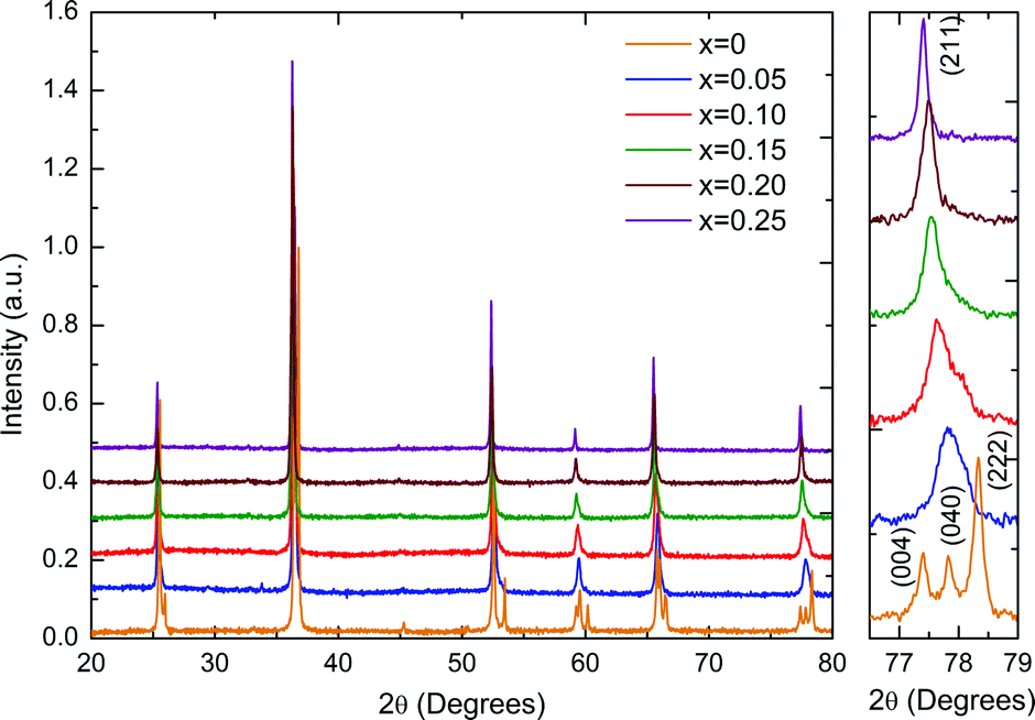 | ||
| Fig. 1 Room-temperature XRD data for (1 − x)KNbO3–x(Ba0.5Bi0.5)(Nb0.5Zn0.5)O3 ceramics (x increases from bottom to top). | ||
For x = 0.05, a shoulder is visible on the higher 2θ side indicating a distortion away from cubic symmetry. This composition still shows an average orthorhombic crystal symmetry. For x = 0.10 and 0.15, XRD data are consistent with the coexistence of an orthorhombic KN-based phase (space group Amm2) and a cubic phase (space group Pmm). The relative content of the orthorhombic phase falls from ∼70% for x = 0.10 to ∼30% for x = 0.15. In both ceramics, the existence of the ferroelectric orthorhombic KN-based phase is also corroborated by the appearance of two dielectric anomalies as a function of temperature, as discussed later. The anomalies are associated with the orthorhombic-to-tetragonal and the tetragonal-to-cubic structural phase transitions. For x = 0.20 and 0.25, the diffraction data are consistent with an average cubic crystal symmetry; however, Raman spectra presented in Fig. 3 demonstrate that actually none of these compositions show a local structure that is truly cubic. Average lattice metrics calculated from the Rietveld refinement of XRD data for all KN-BBNZ ceramics are given in Table S1 of the ESI.† The unit cell volume for the orthorhombic phase (Amm2) increases linearly up to x = 0.10, at this concentration, orthorhombic and cubic symmetries coexist, but beyond this concentration the unit cell volume for the cubic phase also increases linearly, as shown in Fig. 2. The variation in the cell volume for the single-phase compositions follows Vegard's law.
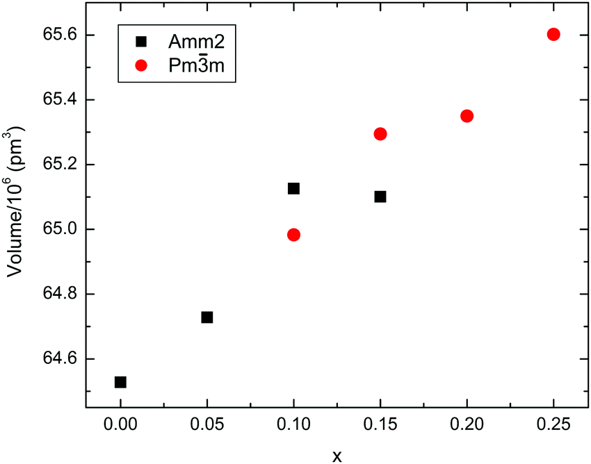 | ||
| Fig. 2 Compositional variation in the unit cell volume for (1 − x)KNbO3–x(Ba0.5Bi0.5)(Nb0.5Zn0.5)O3 (0 ≤ x ≤ 0.25) ceramics. | ||
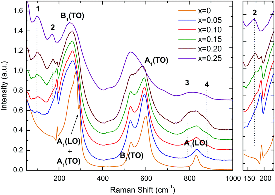 | ||
| Fig. 3 Room-temperature Raman spectra of (1 − x)KNbO3–x(Ba0.5Bi0.5)(Nb0.5Zn0.5)O3 (0 ≤ x ≤ 0.25) ceramics (x increases from bottom to top). | ||
Raman spectroscopy
Room-temperature Raman spectra from KN-BBNZ (0 ≤ x ≤ 0.25) ceramics are presented in Fig. 3. From a group theory analysis, orthorhombic KN (x = 0) exhibits 12 Raman active optical modes of 4A1 + 4B1 + 3B2 + A2 symmetries, which can be separated into translational modes of isolated K+ and internal modes of the NbO6 octahedra.Modes in the KN Raman spectra are labelled according to the single-crystal assignment by Quittet et al.:31 (i) a mixed sharp mode at 192 cm−1; (ii) a Fano-type interference dip at 197 cm−1; (iii) a broad B1(TO) mode centered at 250 cm−1; (iv) a B1(TO) mode at 272 cm−1; (v) a sharp mode at 278 cm−1; (vi) another mode at 294 cm−1; (vii) a B1(TO) mode at ∼532 cm−1; (viii) a A1(TO) mode at ∼600 cm−1 and (ix) a low intensity A1(LO) mode at 831 cm−1. The sharp mode at 192 cm−1 is a mixed B1(TO), A1(TO), A1(LO) and B2(TO) mode. Similarly, the mode at 278 cm−1 is due to a broad A1(TO) combined with a sharp A2, whilst the sharp mode at 294 cm−1 is due to A1(LO) and A1(TO). However because of the resolution limit of the instrument, they appear merged as a single peak. Upon doping new modes emerged, which here are labelled 1, 2, 3 and 4, because at this stage the information on their origin is purely speculative. Mode 1 emerges around ∼100 cm−1, whereas mode 2 appears at ∼175 cm−1, as a shoulder to the sharp mixed mode at 192 cm−1. These modes are fairly static, as they only shift by ∼1 cm−1 over the entire compositional range, but their relative intensity increases continuously. In the past, they have been associated with A–O vibrations within nanometer-sized clusters rich in either Bi3+ and/or K+ cations. Modes 3 and 4 appear on both sides of the high frequency A1(LO) mode. These have been previously associated with breathing of the BO6 octahedra, when occupied by different B-cations. Doping also leads to softening of some modes. For example, the A1(TO) mode at ∼600 cm−1 for x = 0 gradually softens to 585 cm−1 for x = 0.20 due to the increase in the unit cell volume, as shown in Fig. 2. Indeed, softening of this O–Nb–O symmetric stretching mode is known to occur in undoped KN with increasing temperature, as expected from the lattice thermal expansion, which implies a lowering of the force constants. In contrast, the B1(TO) mode at ∼532 cm−1 shows no compositional shift. The relative intensity of the A1(TO) mode in relation to the B1(TO) mode decreases continuously with increasing x. For x = 0.25, the A1(TO) mode is considerably less intense than the B1(TO) mode.
The occurrence of long-range polarisation in KN is ultimately associated with the presence of (i), (ii) and (vi) modes, which therefore can be used to monitor the polar nature of KN-based solid solutions, as shown by Luisman et al.32 Hence, the presence of (i), (ii) and (vi) modes in the spectra of KN-BBNZ ceramics supports the occurrence of spontaneous polarisation in ceramics with x ≤ 0.20. Later, it will be shown through polarisation vs. electric field (P–E) measurements that this polarisation is reversible. Hence, the presence of spontaneous polarisation even in x = 0.20 suggests the presence of some residual orthorhombic (Amm2) phases, but at a level below the detection limit of the in-house XRD. This is consistent with the decrease of the relative intensity of mode (ii) in comparison with mode 2, as illustrated in the expanded region of Fig. 3. The presence of this residual orthorhombic phase is also responsible for dielectric anomalies in x = 0.20 ceramics, as shown later. Finally, the absence of (i), (ii) and (vi) modes from the x = 0.25 spectrum suggests a complete lack of long-range polarisation, which completely rules out the occurrence of ferroelectricity in 0.75KNbO3–0.25(Ba0.5Bi0.5)(Nb0.5Zn0.5)O3. Again, the absence of ferroelectricity will be later corroborated through P–E measurements in combination with strain vs. electric (S–E) curves and dielectric data. Indeed, the absence of a measurable electromechanical response under an electric field as large as 80 kV cm−1, combined with a dielectric response free of anomalies, is consistent with ceramics exhibiting an average cubic crystal symmetry, as determined from XRD traces shown in Fig. 1.
Nevertheless, the presence of intense broad modes in the Raman spectrum of x = 0.25 ceramics, Fig. 3, provides ample evidence that their local crystal symmetry cannot be described by the cubic Pmm space group. The presence of K+, Ba2+ and Bi3+ in A-sites and Nb5+ and Zn2+ in B-sites induces local strains due to not only the difference in ionic radii but also the hybridization between the 6s2 lone-pair of electrons of Bi3+ with both empty 6p0 orbitals of Bi3+ and the 2p6 electrons of O2− which foreshortens the Bi–O covalent bonds. Bi3+ cations in perovskite compounds tend to off-center, often inducing rhombohedral distortions, thereby relieving the tensile bond strain of shorter Bi–O bonds. All the aforementioned local deformations allow for strong Raman scattering on materials, whose average crystal structure may be described by the cubic Pmm space group, since the ions are locally displaced away from the centre of inversion. Octahedral tilting due to smaller Bi3+, which is a common distortion mechanism for reducing the A–O bond strain in perovskites, can be partially counteracted by the equivalent concentration of larger Ba2+ in KN-BBNZ ceramics. In summary, the Raman spectrum for x = 0.25 provides a strong spectroscopic indication of the occurrence of short-range lattice deformations, which could not be resolved from the XRD data but also rules out spontaneous polarisation in those ceramics. In addition, in situ Raman analysis between −180 and 280 °C suggested that the crystal symmetry for x = 0.25 is unchanged in this temperature range, in contrast to KNbO3, as shown in Fig. S7 in the ESI.† Finally, the increasing broadening of modes in the Raman spectra with increasing x is consistent with increasing lattice disorder, which may be behind the dielectric response and the emergence of Urbach tails in optical response, as discussed later.
Dielectric and electromechanical properties
The temperature dependence of the permittivity, εr, for KN-BBNZ ceramics (x = 0, 0.05, 0.10, 0.15, 0.20 and 0.25) measured at 100 kHz is illustrated in Fig. 4. This gives a general overview on the impact of doping in phase transitions. Interestingly, all doped compositions exhibit a larger εr at lower temperatures than pure KN, but which decreases with increasing x.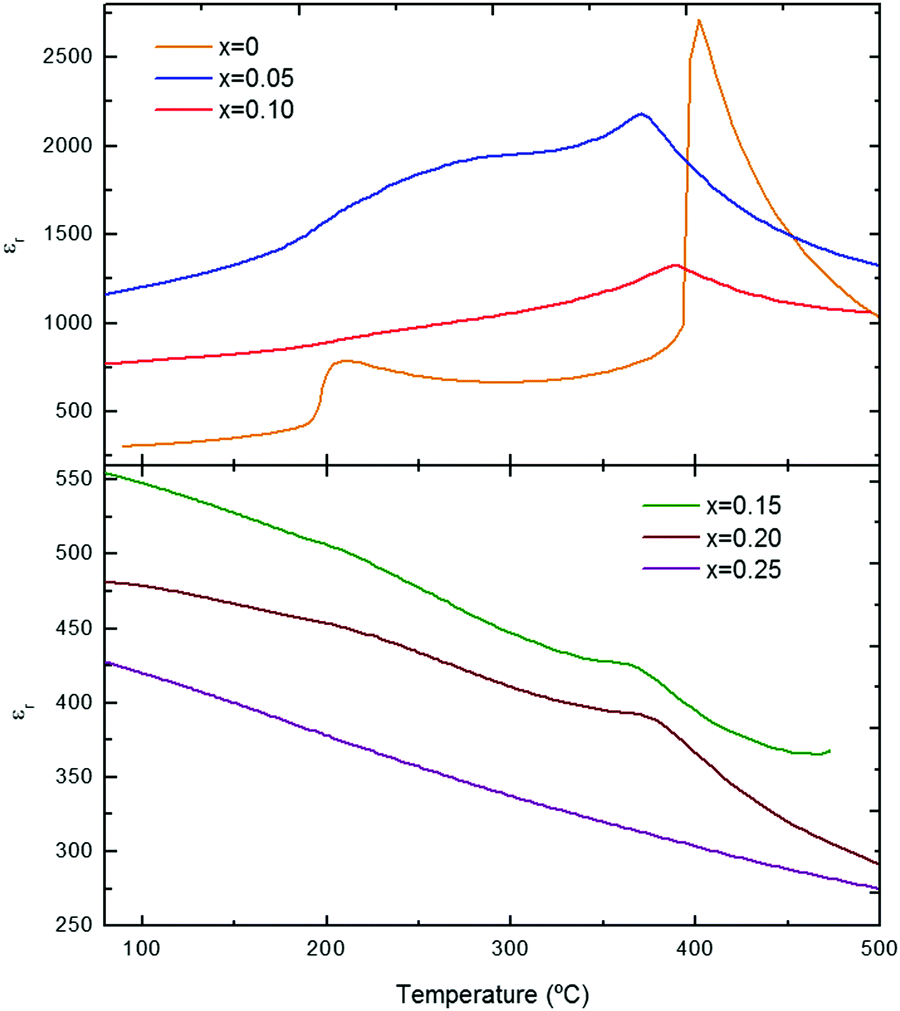 | ||
| Fig. 4 Temperature dependence of εr for (1 − x)KNbO3–x(Ba0.5Bi0.5)(Nb0.5Zn0.5)O3 (0 ≤ x ≤ 0.25) ceramics. | ||
KN (x = 0) shows two maxima at ∼205 °C and ∼400 °C, respectively. Those two dielectric anomalies are associated with the orthorhombic-to-tetragonal and the tetragonal-to-cubic structural phase transitions, respectively. The highest temperature maximum corresponds to the Curie temperature, Tc. Upon increasing x, Tc initially drops to ∼370 °C for x = 0.05, then it increases to ∼387 °C for x = 0.10, subsequently dropping to ∼370 °C for x = 0.15. This non-monotonic Tc variation occurs within the multiphase composition range, which suggests a non-homogeneous distribution of dopants between the orthorhombic and cubic phases. As aforementioned, x = 0.20 still shows dielectric anomalies due to a residual orthorhombic phase, which was not detected in the XRD traces because it is present at levels below the detection limit of the technique. Finally, for x = 0.25, εr decreases continuously upon increasing the temperature. No dielectric anomalies are detected in this temperature range, as expected from the XRD data, Fig. 1, which suggests that this composition has an average cubic crystal structure. Nevertheless, it is worth noting that the εr is considerably large for a truly cubic structure, in agreement with the Raman analysis, which points out the occurrence of local distortions. Frequency-dependent measurements of the relative permittivity and dielectric loss are provided for individual compositions in the ESI,† Fig. S8. KN (x = 0) shows a room-temperature εr of ∼300, as shown in Fig. S8a (ESI†). A strong frequency dependence of both εr and tan δ is observed for x = 0.05 and 0.10, as illustrated in Fig. S8b and c (ESI†), respectively. The temperature for the εr anomalies remains almost unaltered, but their magnitude decreases upon increasing the frequency. Since tan δ also decreases upon increasing the frequency, this frequency dependency is different from that observed for conventional relaxors such as Pb(Mg1/3Nb2/3)O3. Nevertheless, it is consistent with the results observed for some KNN-based solid solutions.27 For x ≥ 0.15, the frequency dependence is much less pronounced, as shown in Fig. S8d and e (ESI†).
Polarisation vs. electric field (P–E) and strain vs. electric field (S–E) loops of KN-BBNZ ceramics measured at room temperature under an electric field of 80 kV cm−1 are shown in Fig. 5. Undoped KN (x = 0) exhibits a P–E loop typical of a ferroelectric response, as shown in Fig. 5.
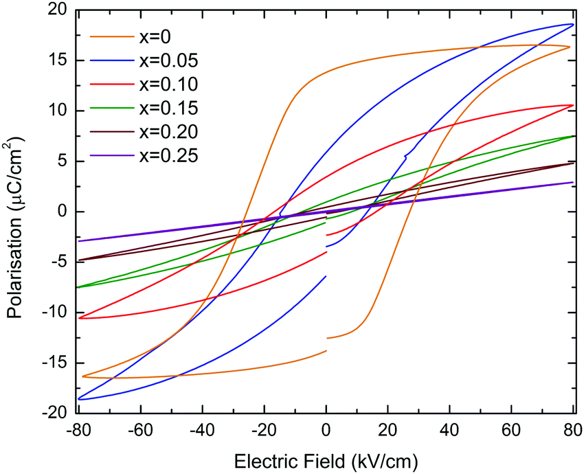 | ||
| Fig. 5 P–E measurements for (1 − x)KNbO3–x(Ba0.5Bi0.5)(Nb0.5Zn0.5)O3 (0 ≤ x ≤ 0.25) ceramics. | ||
KN ceramics show a maximum polarisation, Pmax, of ∼16.4 μC cm−2, a remnant polarization, Pr, of ∼13.8 μC cm−2 and a coercive field, Ec, of ∼26 kV cm−1. When (Ba0.5Bi0.5)(Nb0.5Zn0.5)O3 is substituted into the KN lattice, both Pr and Ec decrease dramatically and the P–E loops become increasingly slimmer as shown in Fig. 5, whereas the S–E curves evolve from a butterfly shape (which is typical for the FE response due to domain switching) to a parabolic shape (as expected for an electrostrictive response), as shown in Fig. 6.
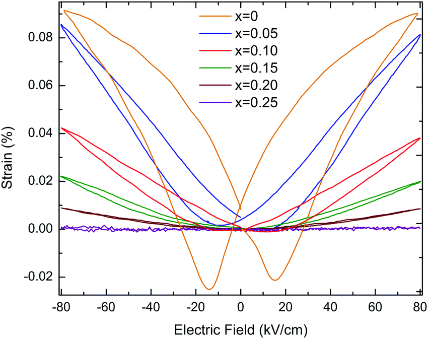 | ||
| Fig. 6 S–E measurements for (1 − x)KNbO3–x(Ba0.5Bi0.5)(Nb0.5Zn0.5)O3 (0 ≤ x ≤ 0.25) ceramics. | ||
The bipolar electric-field induced strain for KN (x = 0) reaches about 0.091% under a field of 80 kV cm−1, as shown in Fig. 6. The strain curve shows that the negative strain can reach ∼0.02%, which is due to the ferroelectric domain and domain wall switching. For x = 0.05, Pr is ∼6 μC cm−2, which is roughly 2.5 times smaller than for KN, the maximum achievable strain under an electric field of 80 kV cm−1 is ∼0.082%. For the multiphasic (orthorhombic + cubic) x = 0.10, 0.15 and 0.20, S–E responses show almost parabolic shapes, as shown in Fig. 6, and their maximum achievable strains drop to ∼0.041%, 0.021% and 0.009%, respectively (ESI,† Fig. S9). This electrostrictive-like response can be modelled according to the S = QP2 relationship, where S, Q and P represent the strain, electrostriction coefficient and polarisation, respectively. For example for x = 0.05, Q was calculated to be 0.023 m4 C−2 (ESI,† Fig. S10). This value is even larger than that of the well-known electrostrictive material 0.93Pb(Mg1/3Nb2/3)O3–0.07PbTiO3 (PMN-7PT) which has Q of 0.017 m4 C−2 with a maximum strain of 0.12% at 40 kV cm−1. However, the value of strain of x = 0.05 is comparatively low. Electrostriction in Pb-free materials has been investigated in recent years.33–36Q values ranging from 0.021 to 0.027 m4 C−2 were reported in Bi0.5Na0.5TiO3–BaTiO3–K0.5N0.5NbO3 ceramics.37 More recently, Pb-free ferroelectric ceramics have been reported to exhibit giant electrostrictive coefficients as large as 0.05 m4 C−2.38 The temperature dependence of the electric-field induced strain for x = 0.05 is moderate (∼13%), as illustrated by the unipolar measurements in the ESI,† Fig. S11. Finally, for single-phase x = 0.25 with an average cubic structure, the P–E curve is virtually linear (hysteresis free) and a maximum polarisation of ∼2.9 μC cm−2 is measured at 80 kV cm−1, as shown in Fig. 5. This composition does not show any measurable field-induced strain, as shown in Fig. 6. At this stage, it is still unclear why x = 0.05 shows a higher field-induced maximum polarisation than KN, but a lower field-induced strain. Many reasons such as grain size and orientation, domain size and density can be speculated to be at the origin of this counterintuitive result.
Hence, the piezoelectric response for KN (x = 0) arises from the macroscopic absence of a center of symmetry, and the butterfly-shaped S–E curves are due to domain switching, whereas for x = 0.05 the banana-shaped response is associated with nanoregions with fluctuating polarisation (which may be associated with Raman modes 1 and 2 in Fig. 3). Indeed, the lone-pair of electrons brought by Bi3+ may play an important role in this nanodomain process, possibly through the adjustment of the orientation of the lone-pair and the associated dipole moment with the applied electric field. The polar nanoregions respond to the applied electric field and may grow up to the microscale.
The piezoelectric-to-electrostrictive crossover in the KNbO3–(Ba0.5Bi0.5)(Nb0.5Zn0.5)O3 system can be interpreted by the competition induced by a mixture of covalent and ionic bonds and a distribution of effective cation radii which occurs due to the presence of K+, Bi3+ and Ba2+ in A-sites and Nb5+ and Zn2+ in B-sites of the perovskite structure. The incorporation of Zn2+ in B-site disrupts the Nb–O bonding, which is responsible for the long-range ordered displacement of Nb5+. This gives rise to a distribution of bond lengths, and this lattice disturbance affects the balance between long-range dipolar Coulombic forces and short-range repulsion forces, which determines the occurrence of ferroelectricity in the perovskite structure. Disruption of this balance is ultimately responsible for the disappearance of the long-range polar ordering, as indicated by the absence of the 192 cm−1 sharp mode from the Raman spectrum of x = 0.25. In the x = 0.10–0.20 range, the field-induced strain decreases because of the increasing volume fraction of the cubic phase which, in contrast to previous first-principles calculations, was proved to be non-ferroelectric.
Optical band gaps
The excitation across the band gap in KN-BBNZ ceramics is essentially a charge transfer from the O 2p states at the valence band maximum (VBM) to the transition-metal d states at the conduction band minimum (CBM). Some insight into the band structure and other charge transitions can be gathered from the response to photons of different energies. Here, diffuse reflectance spectroscopy was carried out using photons with wavelengths ranging from 200 to 1600 nm. The band gaps for KN-BBNZ ceramics were determined using the Tauc plot in Fig. 7 and are listed in Table S2 in the ESI.†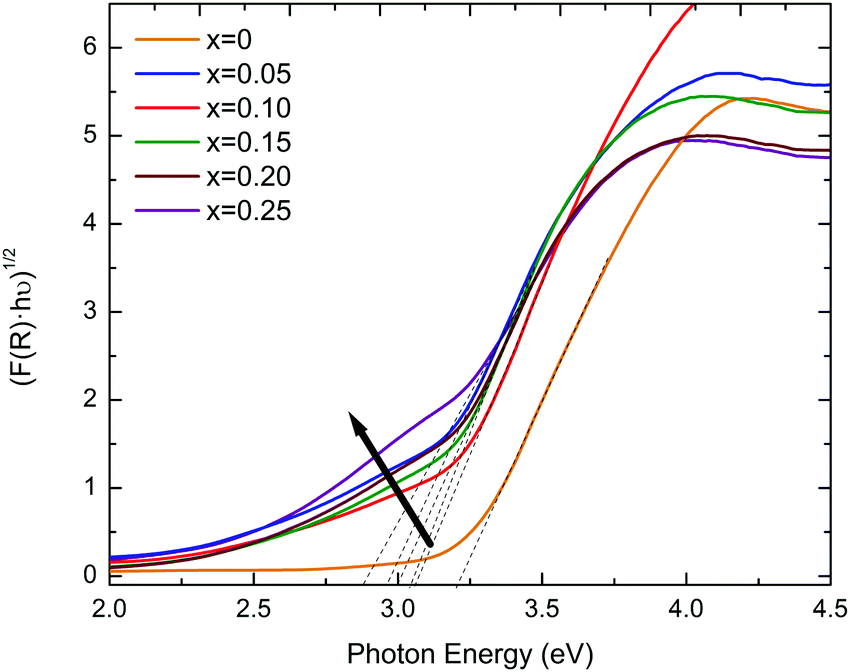 | ||
| Fig. 7 Tauc’s plot for indirect band gaps for (1 − x)KNbO3–x(Ba0.5Bi0.5)(Nb0.5Zn0.5)O3 (0 ≤ x ≤ 0.25) ceramics. | ||
The band gap energies were obtained from the intercept of the tangent line in the plot of [hνF(R)]1/2vs. energy. The indirect band gap of (1 − x)KNbO3–x(Ba0.5Bi0.5)(Nb0.5Zn0.5)O3 (0 ≤ x ≤ 0.25) ceramics varies from 3.22 eV for x = 0 to 2.89 eV for x = 0.25, in broad agreement with the first-principles calculations,25 and also with experimental results for KNbO3.4,39 Moreover, these band gaps are consistent with the ability of KN-BBNZ ceramics to withstand electric fields as high as 80 kV cm−1, as previously shown in Fig. 5 and 6.
Crystal chemistry arguments can be recalled to explain the moderate band gap narrowing as follows: (i) the replacement of Nb5+ by Zn2+ creates underbonded O2− ions adjacent to the Zn2+, which form ZnO6 octahedra, (ii) Bi3+ ions which tend to be off-center, create short, strong Bi–O (covalent) bonds that partially compensate for the aforementioned loss of B–O bonding and (iii) Ba2+ ions are not off-center and are less prone to compensate the decrease of B–O bonding. As a result, the repulsion between the non-bonding O charge densities and Zn 3d states is relatively weak, leading to a moderate upshift of valence band maxima (VBM), which is composed of O 2p and Zn 3d states.25
It is worth noting that the observed Raman shift of the broad A1(TO1), Fig. 3, may be a manifestation of the strong Bi–O bonds, whereas the general broadening of Raman modes results from an increased lattice disorder, which manifests itself by the emergence of Urbach tails, as indicated by an arrow in Fig. 7. From the analysis of the Urbach tails, it is possible to obtain the information pertaining to the dynamics of the electronic transitions, and in principle to evaluate the impact of defects on those transitions. For example, the Urbach energy, Eu, for KN-BBNZ when x = 0.25 was calculated as 0.22 eV.
In summary, a combination of competition between covalent and ionic bonds and a distribution of effective cation radii in the KNbO3–(Ba0.5Bi0.5)(Nb0.5Zn0.5)O3 system leads simultaneously to a piezoelectric-to-electrostrictive crossover and a modest narrowing of the optical band gaps.
Conclusions
The band gap evolution and the piezoelectric-to-electrostrictive crossover in the (1 − x)KNbO3–x(Ba0.5Bi0.5)(Nb0.5Zn0.5)O3 ceramics arise from a distribution of bond lengths brought in by the larger Ba2+ and K+ ions, which create oversized A-site cages for Bi3+ ions. This results in off-centering of Bi3+ in order to create shorter Bi–O bonds and thereby relieve the tensile bond strain. Zn2+ ions in B-sites also lead to substantial lattice disorder, resulting in a gradual disappearance of long-range reversal polarisation and a moderate narrowing of the optical band gap, by a moderate upshift of the VBM. The band gap of KN-BBNZ when x = 0.25 is 2.89 eV, which is in agreement with previous first-principles calculations;25 however, it is non-ferroelectric at room temperature.Acknowledgements
Cristina Pascual-Gonzalez acknowledges the financial support of a VC scholarship from SHU. Ian M. Reaney acknowledges the support of the Engineering and Physical Sciences Research Council through EP/L017563/1.References
- F. Wang, I. Grinberg, L. Jiang, S. Young, P. Davies and A. Rappe, Ferroelectrics, 2015, 483, 1–12 CrossRef CAS.
- T. Zhang, K. Zhao, J. Yu, J. Jin, Y. Qi, H. Li, X. Hou and G. Liu, Nanoscale, 2013, 5, 8375–8383 RSC.
- J. Lombardi, F. Pearsall, W. Li and S. O'Brien, J. Mater. Chem. C, 2016, 4, 7989–7998 RSC.
- P. Wu, G. Wang, R. Chen, Y. Guo, X. Ma and D. Jiang, RSC Adv., 2016, 6, 82409–82416 RSC.
- G. Wang, Y. Huang, A. Kuang, H. Yuan, Y. Li and H. Chen, Inorg. Chem., 2016, 55, 9620–9631 CrossRef CAS PubMed.
- Y. Wang, X. Kong, W. Tian, D. Lei and X. Lei, RSC Adv., 2016, 6, 58401–58408 RSC.
- A. Bhatnagar, A. Chaudhuri, Y. Kim, D. Hesse and M. Alexe, Nat. Commun., 2013, 4, 2835 CrossRef.
- Q. Fu, X. J. Wang, C. Y. Li, Y. Sui, Y. P. Han, Z. Lv, B. Song and P. Xu, RSC Adv., 2016, 6, 108883 RSC.
- B. Modak and S. Ghosh, RSC Adv., 2016, 6, 9958–9966 RSC.
- I. Grinberg, D. West, M. Torres, G. Gou, D. Stein, L. Wu, G. Chen, E. Gallo, A. Akbashev, P. Davies, J. Spanier and A. Rappe, Nature, 2013, 503, 509–512 CrossRef CAS PubMed.
- G. Shirane, H. Danner, A. Pavlovic and R. Pepinsky, Phys. Rev., 1954, 93, 672–673 CrossRef CAS.
- C. Pascual-Gonzalez, G. Schileo and A. Feteira, Appl. Phys. Lett., 2016, 109, 9132902 CrossRef.
- D. Kim, M. Joung, I. Seo, J. Hur, J. Kim, B. Kim, H. Lee and S. Nahm, J. Eur. Ceram. Soc., 2014, 34, 4193–4200 CrossRef CAS.
- H. Birol, D. Damjanovic and N. Setter, J. Am. Ceram. Soc., 2005, 88, 1754–1759 CrossRef CAS.
- K. Kakimoto, I. Masuda and H. Ohsato, J. Eur. Ceram. Soc., 2005, 25, 2719–2722 CrossRef CAS.
- J. Kim, D. Kim, I. Seo, J. Hur, J. Lee, B. Kim and S. Nahm, Sens. Actuators, A, 2015, 234, 9–16 CrossRef CAS.
- J. Acker, H. Kungl and M. Hoffmann, J. Eur. Ceram. Soc., 2013, 33, 2127–2139 CrossRef CAS.
- K. Matsumoto, Y. Hiruma, H. Nagata and T. Takenaka, Ceram. Int., 2008, 34, 787–791 CrossRef CAS.
- X. Lv, Z. Y. Li, J. G. Wu, D. Q. Xiao and J. G. Zhu, ACS Appl. Mater. Interfaces, 2016, 8, 30304–30311 CAS.
- M. R. Joung, H. B. Xu, I. T. Seo, D. H. Kim, J. Hur, S. Nahm, C. Y. Kang, S. J. Yoon and H. M. Park, J. Mater. Chem. A, 2014, 2, 18547–18553 CAS.
- Y. Yang, J. Jung, B. Yun, F. Zhang, K. Pradel, W. Guo and Z. Wang, Adv. Mater., 2012, 24, 5357–5362 CrossRef CAS PubMed.
- J. Jung, C. Chen, B. Yun, N. Lee, Y. Zhou, W. Jo, L. Chou and Z. Wang, Nanotechnology, 2012, 23, 375401 CrossRef PubMed.
- L. Yu, J. Jia, G. Yi, Y. Shan and M. Han, Mater. Lett., 2016, 184, 166–168 CrossRef CAS.
- F. Wang and A. Rappe, Phys. Rev. B: Condens. Matter Mater. Phys., 2015, 91, 165124 CrossRef.
- F. Wang, I. Grinberg and A. Rappe, Phys. Rev. B: Condens. Matter Mater. Phys., 2014, 89, 235105 CrossRef.
- V. V. Shvartsman and D. C. Lupascu, J. Am. Ceram. Soc., 2012, 95, 1–26 CrossRef CAS.
- Y. P. Guo, K. Kakimoto and H. Ohsato, Solid State Commun., 2004, 129, 279–284 CrossRef CAS.
- H. L. Du, W. C. Zhou, F. Luo, D. M. Zhu, S. B. Qu, Y. Li and Z. B. Pei, J. Appl. Phys., 2008, 104, 034104 CrossRef.
- S. Priya and S. Nahm, Lead-Free Piezoelectrics, Springer, New York, 2011 Search PubMed.
- J. Acker, H. Kungl, R. Schierholz, S. Wagner, R. Eichel and M. Hoffmann, J. Eur. Ceram. Soc., 2014, 34, 4213–4221 CrossRef CAS.
- A. Quittet, M. Bell, M. Krauzman and P. Raccah, Phys. Rev. B: Condens. Matter Mater. Phys., 1976, 14, 5068–5072 CrossRef CAS.
- L. Luisman, A. Feteira and K. Reichmann, Appl. Phys. Lett., 2011, 99, 192901 CrossRef.
- W. Bai, L. Li, W. Wang, B. Shen and J. Zhai, Solid State Commun., 2015, 206, 22–25 CrossRef CAS.
- F. Wang, C. Jin, Q. Yao and W. Shi, J. Appl. Phys., 2013, 114, 027004 CrossRef.
- R. Z. Zuo, H. Qi, J. Fu, J. F. Li, M. Shi and Y. D. Xu, Appl. Phys. Lett., 2016, 108, 142902 CrossRef.
- S. T. Zhang, F. Yan, B. Yang and W. W. Cao, Appl. Phys. Lett., 2010, 97, 142902 CrossRef.
- S. T. Zhang, A. B. Kounga, W. Jo, C. Jamin, K. Seifert, T. Granzow, J. Rodel and D. Damjanovic, Adv. Mater., 2009, 21, 4716–4720 CrossRef CAS.
- L. Jin, R. J. Huo, R. P. Guo, F. Li, D. W. Wang, Y. Tian, Q. Y. Hu, X. Y. Wei, Z. B. He, Y. Yan and G. Liu, ACS Appl. Mater. Interfaces, 2016, 8, 31109–31119 CAS.
- H. Shi, C. Zhang, C. Zhou and G. Chen, RSC Adv., 2015, 5, 93615–93622 RSC.
Footnote |
| † Electronic supplementary information (ESI) available: XRD, Raman, SEM water immersion test and Tauc plot data for stoichiometric KNbO3 and K-deficient K0.95NbO3 ceramics and XRD, Tauc plot, SEM, Raman, Permittivity and electromechanical data for KN-BBNZ ceramics. See DOI: 10.1039/c6tc05515j |
| This journal is © The Royal Society of Chemistry 2017 |