
Ambience dependent photoluminescence reveals the localization and trap filling effects in CH3NH3PbI3−xClx perovskite films†
Jing
Li
,
Qianqian
Yu
,
Bin
Lu
,
Haiping
He
 * and
Zhizhen
Ye
* and
Zhizhen
Ye
State Key Laboratory of Silicon Materials, School of Materials Science and Engineering, Zhejiang University, Hangzhou 310027, People's Republic of China. E-mail: hphe@zju.edu.cn
First published on 29th November 2016
Abstract
The photophysics of organolead trihalide perovskites are still not fully understood. Here we report that the photoluminescence (PL) lineshape, decay features, and intensity of solution-processed CH3NH3PbI3−xClx films are highly sensitive to the ambience. The radiative recombination actually consists of two decay channels corresponding to recombination of extended and localized states, respectively. The PL decay can be well described by a model considering the carrier localization, surface band bending, and trapping–detrapping of carriers.
Introduction
Organolead trihalide perovskite semiconductors CH3NH3PbX3 (X = I, Cl, Br) have continuously attracted extensive attention due to their unique and excellent properties for both photovoltaic1–4 and light-emitting devices.5–10 High luminescence efficiency is realized in this class of materials. Deschler et al.6 reported photoluminescence quantum efficiencies (PLQEs) as high as 70% at high excitation densities. Cho et al.8 demonstrated light-emitting diodes (LEDs) with an external quantum efficiency of 8.53%. Most strikingly, optically pumped lasing with very low thresholds was observed by several groups.6,11,12 Nevertheless, less is known about the mechanism of the high performance of perovskite-based devices, and fundamental studies on these materials are desired.Among those fundamental issues, the recombination of photocarriers is of critical importance. However, the photophysics of organolead trihalide perovskites are rather complicated. Recently there have been several reports13–17 assigning the PL to free carrier (FC) recombination. In such a framework, the decay features were interpreted using trap-involved models.14,17 Such models predict nearly exponential PL decay at excitation densities lower than the trap density. However, various shapes of PL decay curves were experimentally observed. Since CH3NH3PbX3 perovskites are usually processed from solutions close to room temperature, a high defect density is unavoidable.18 In such samples, disorder and carrier localization are expected to be present. Indeed, the localization effect has been revealed by terahertz photoconductivity19 and PL measurements.20 Therefore, more effects such as carrier localization and trapping–detrapping21 should be considered in the recombination dynamics. In this work, we carried out steady-state and time-resolved PL measurements both in air and in a vacuum to gain a deep understanding of the recombination of photocarriers. We find a clear non-exponential PL decay at an excitation density even as low as 1013 cm−3 and PL features highly sensitive to the ambience. We propose a model involving carrier localization and trap filling effects to interpret the experimental results.
Experimental section
The samples used for PL studies are CH3NH3PbI3−xClx films synthesized using a two-step solution process. All the ITO coated glass substrates were cleaned sequentially with deionized water, ethanol, acetone and oxygen plasma before spin-coating. Methylamine iodide (MAI) was prepared by reacting methylamine, 33 wt% in ethanol (Sigma-Aldrich), with hydroiodic acid (HI) 57 wt% in water (Sigma-Aldrich), at room temperature. HI was added dropwise while stirring. Upon drying at 100 °C, the resultant white powder was dried overnight in a vacuum oven and recrystallized from ethanol before use. To form the CH3NH3PbI3−xClx precursor solution, methylammonium iodide and lead(II) chloride (Sigma-Aldrich) were dissolved in anhydrous N,N-dimethylformamide (DMF) at a 3![[thin space (1/6-em)]](https://www.rsc.org/images/entities/char_2009.gif) :1 molar ratio of MAI to PbCl2, with final concentrations of 0.88 M lead chloride and 2.64 M methylammonium iodide. The precursor was filtered through a 220 nm PTFE filter head, and then spin-coated at 3000 rpm for 30 seconds on an ITO coated glass; finally, it was annealed at 95 °C for ∼10 min.
:1 molar ratio of MAI to PbCl2, with final concentrations of 0.88 M lead chloride and 2.64 M methylammonium iodide. The precursor was filtered through a 220 nm PTFE filter head, and then spin-coated at 3000 rpm for 30 seconds on an ITO coated glass; finally, it was annealed at 95 °C for ∼10 min.
To minimize the degradation induced by air exposure, the films were prepared and kept in a glove box before PL measurements. The steady-state and time-resolved PL measurements were performed on a FLS920 fluorescence spectrophotometer (Edinburgh Instruments). In order to obtain information about defects correctly, and to avoid any effects induced by high density free carriers, we restrict our experiments to the low excitation level. A semiconductor pulsed laser working at a wavelength of 638.8 nm, a pulse width of 86.4 ps, and a repeating frequency of 200 kHz–20 MHz was used as the excitation source. The excitation fluence used for steady-state and time-resolved PL measurements is 4 and 0.04 nJ cm−2, which corresponds to a photocarrier density of ∼1015 and ∼1013 cm−3, respectively. Such excitation densities are relatively low and comparable to the working regime of photovoltaic devices.13,17 PL decay was recorded using the time-correlated single photon counting (TCSPC) technique. The measurements in air are carried out with a humidity of 40–50%. After that the sample chamber is pumped to 1 Pa in 10 min for vacuum measurements. All measurements were performed at room temperature. The ultraviolet photoelectron spectroscopy (UPS) was performed on a KRATOS AXIS Ultra DLD spectrometer using He I (21.2 eV) as the excitation source.
Results and discussion
Interestingly, we found clear difference between the PL spectra recorded in air and in a vacuum. Although the PL peaks are almost the same, the high-energy wing of the PL in a vacuum is higher than that in air (Fig. 1a). In addition, the PL intensity in a vacuum is significantly lower than that in air. Most strikingly, the PL decay in air is remarkably different from that in a vacuum. Both of them can be well described by the thermalized stretching exponential decay.22 | (1) |
 | ||
| Fig. 1 (a) PL spectra of CH3NH3PbI3−xClx films in air and in a vacuum. The intensities have been normalized to show the change in the lineshape. The inset shows the two respective PL spectra revealing the relative intensity. (b) PL decay of the films in air and in a vacuum. The solid lines are stretched exponential fits. | ||
The results of Fig. 1 suggest that the PL in a vacuum actually consists of two components. In order to confirm this, we carried out a series of time-resolved PL measurements at various emission wavelengths, as shown in Fig. 2a. It is found that the weight of the fast decay component increases at higher emission energy. From Fig. 2a the PL spectra at different delay times can be acquired (Fig. 2b). At the initial stage after the excitation stops, the high-energy wing of the PL spectra is higher, resulting in an obvious asymmetric lineshape. As the delay time increases, it decreases quickly and becomes constant at t > 100 ns. For the PL in air, however, the PL spectra at different delay times are identical and do not show any increase of the high-energy wing (Fig. S1 in the ESI†). These results strongly indicate that the fast component in PL decay is from the high-energy wing of the PL, while the broad and nearly symmetric PL is responsible for the slow decay component. The fast component represents intrinsic recombination because of its higher emission energy, while the slow one is most likely associated with localized states induced by defects, impurities or disorder in the films. We note that defects in semiconductors can be either radiative or nonradiative, and the radiative localized states are different from the nonradiative traps which will be discussed later. Emissions from localized states have been widely reported for other semiconductors.22,23 We also note that the possible contribution of PbI2, which may be formed due to the decomposition of perovskite in the presence of water in air,24,25 to the higher-energy wing of PL can be neglected because no interband transition of PbI2 is detected near 2.3 eV and no PbI2 phase is detected by X-ray diffraction (Fig. S2, ESI†).
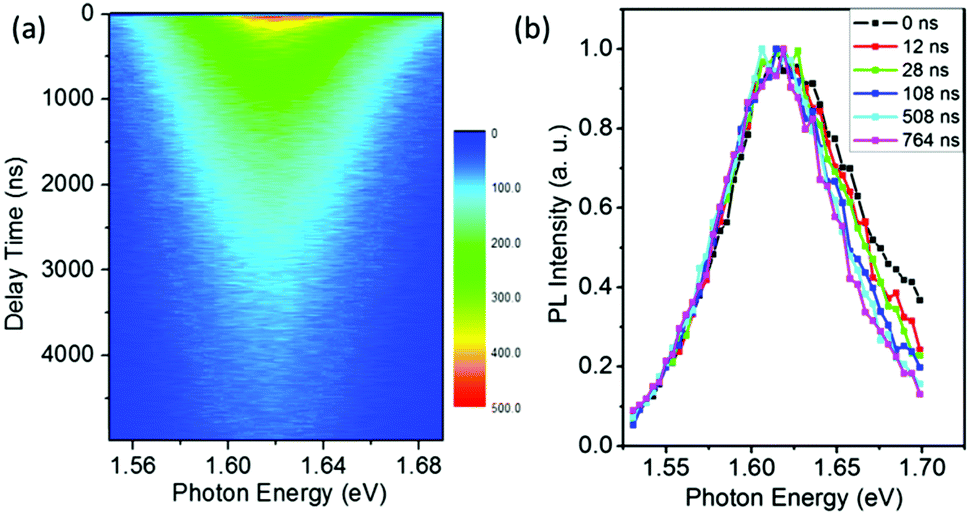 | ||
| Fig. 2 (a) Time-resolved emission spectra (TRES) of CH3NH3PbI3−xClx films in a vacuum. (b) Normalized PL spectra at various delay times. The peak of the decay curves is set at t = 0. The evolution of the high-energy wing at the initial stage of the PL decay is clearly seen, while the peak energy remains almost unchanged. | ||
To study the defects in the films, the time evolution of PL intensity under continuous excitation is recorded both in air and in a vacuum, as shown in Fig. 3. Very interestingly, the PL shows contrary development with illumination time. The PL in air gradually increases with illumination time and saturates when t > 100 s. Such behavior has been reported17,26 in organolead trihalide perovskites and is interpreted as trap filling by the photocarriers or photo-induced migration of halide. However, the PL in a vacuum reaches the maximum immediately after the excitation, then gradually decreases and is also stable when t > 100 s. The photo-induced migration of halide is hard to account for for such contrary phenomena. Both data can be fitted well by bi-exponential decay with similar characteristic times, indicating the same contributing trap states in air and in a vacuum. The long characteristic times on the order of seconds suggest the deep level of these trap states.27 The contrary behavior shown in Fig. 3 indicates that the time scale of the carrier trapping–detrapping process is between the fast and slow PL lifetimes. These results again support our conclusion that the vacuum PL consists of two components.
 | ||
| Fig. 3 Development of PL intensity of CH3NH3PbI3−xClx films in air and in a vacuum under continuous illumination. The PL intensity has been normalized to the maximum in each case. The solid curves represent bi-exponential fits to the data. | ||
The results of Fig. 3 indicate that the recombination of photocarriers is strongly affected by trap states. The actual trap density in our samples is unknown. However, we estimate a density of ∼1015 cm−3 or higher because the traps are not fully occupied quickly under an excitation density of 1015 cm−3. The estimation is reasonable because it is close to the reported value, ∼1016 cm−3, in solution-processed perovskites.11 Such a trap density is much greater than the photocarrier density in our lifetime measurements, 1013 cm−3 (0.04 nJ cm−2). According to the models of Yamada et al.14 and Stranks et al.,17 the PL decay at an excitation density much lower than the density of traps should be nearly exponential. This obviously fails to describe the one in a vacuum. Therefore, an additional mechanism should be considered to interpret the decay features.
The broadening of the high-energy wing in PL spectra is a characteristic feature of FC recombination, while the broad and nearly symmetric emission at lower energy with a much longer lifetime could be attributed to transitions involving localized states. A similar interpretation has been proposed recently by Saba et al.28 By considering the marked change when the measurements are switched from air to vacuum, and keeping in mind that the properties of organolead trihalide perovskites are highly sensitive to the surrounding ambience, we propose a model taking into account the surface band bending to interpret the experimental results. The surface band bending is confirmed by the UPS measurement. As shown in Fig. 4, the spectrum gives a work function of 4.9 eV and a Fermi level of 1.1 eV above the valence band. Taking an electron affinity and valence band maximum of 3.8 and −5.4 eV, respectively,7 the results indicate a slight downward surface band bending of 0.6 eV. We expect more marked bending when the samples are exposed to air, because the adsorption of water molecules may decompose the perovskites by accepting holes. Such hole traps could be, for example, the undercoordinated halides (X−) as suggested by Abate et al.29 On the other hand, the possible self-oxidation of PbII to PbIV also consumes holes.30 These processes result in marked downward surface band bending, leading to the accumulation of electrons in the surface region, as shown in Fig. 5. The localized states are assumed to be present mainly in the surface region considering the nanocrystalline nature of the film. The accumulated electrons can then easily relax into the localized states, followed by their recombination with holes in the valence band. At a low excitation level and in the presence of hole traps, the wavefunction overlap between holes and localized electrons is small, resulting in a low recombination rate and a long PL lifetime.
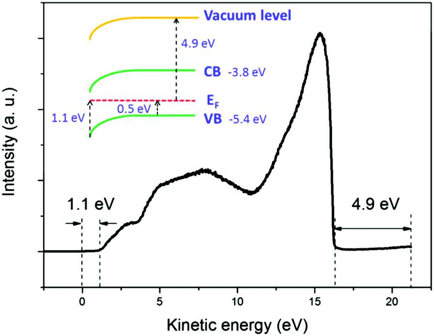 | ||
| Fig. 4 UPS spectrum of the CH3NH3PbI3−xClx film. The work function is determined to be 4.9 eV, and in the surface region the Fermi level locates at 1.1 eV above the valence band. The inset shows the energy diagram of the film. In this diagram, the electron affinity is taken as 3.8 eV and the valence band maximum is accordingly placed at −5.4 eV. The results reveal a downward surface band bending of 0.6 eV in a vacuum. | ||
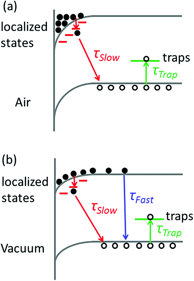 | ||
| Fig. 5 Proposed mechanism for photocarrier recombination (a) in air and (b) in a vacuum. The downward surface band bending induces electron accumulation in the surface region. At a low excitation level, the electron accumulation in (a) is complete. Electrons can relax into localized states and recombine with holes in the valence band (lifetime τSlow). In a vacuum, the surface band bending decreases and the weight of free carrier recombination (lifetime τFast) increases. Holes can suffer a trapping–detrapping process with characteristic time τTrap. | ||
When the samples are put in a vacuum, however, the surface band bending is expected to be reduced due to the isolation from water molecules. In this case, the electrons are no longer completely localized in the surface region, and the FC recombination coexists with the recombination between localized electrons and holes. The model can account for the decreased PL intensity in a vacuum, as shown in Fig. 1a, because the rate of FC recombination is reported to be low in CH3NH3PbI3−xClx perovskite films.31 The model can also interpret the time-evolution of PL intensity in Fig. 3 if we assume that the trapping–detrapping process of holes is slower than the FC recombination but faster than the recombination of localized states. In this case, the photocarriers will first recombine to emit photons before they are trapped. While in air, the photocarriers will be trapped before they can relax into localized states and give luminescence.
The immediate change in the PL lifetime when the ambience is switched to vacuum strongly favors the model of surface adsorption and band bending. This model predicts that the PL features will be reversible when the ambience is switched between air and vacuum. This effect is indeed observed, as evidenced by the PL lifetime measurements (Fig. S3, ESI†). When the ambience is switched back to air again, the PL decay trace can be recovered. This result reinforces the rationality of our proposed model.
Conclusions
In summary, we have studied the photocarrier recombination of solution-processed CH3NH3PbI3−xClx perovskites in air and in a vacuum by means of steady-state and time-resolved PL. We revealed that the PL lineshape and decay, as well as the PL development under continuous excitation, are highly sensitive to the ambience. Compared with the results in air, the PL in a vacuum shows an increased high-energy wing and non-exponential decay. At a low excitation level, the PL actually consists of two radiative recombination channels, i.e., the fast free carrier recombination with a lifetime in the nanosecond scale, and the slow localized state recombination with a lifetime in the microsecond scale. The overall PL features are well described by a simple model considering the electron localization, surface band bending, and single-carrier trapping. Our findings provide deep insights into the fundamental photophysics of organolead trihalide perovskite semiconductors, which will shed new light on the development of high efficiency optoelectronic devices based on this class of materials.Acknowledgements
This work was financially supported by the Natural Science Foundation of Zhejiang Province (No. LY17A040008) and the National Natural Science Foundation of China (No. 51372223 and 91333203).Notes and references
- A. Kojima, K. Teshima, Y. Shirai and T. Miyasaka, J. Am. Chem. Soc., 2009, 131, 6050 CrossRef CAS PubMed.
- G. Hodes, Science, 2013, 342, 317 CrossRef CAS PubMed.
- J. Burschka, N. Pellet, S.-J. Moon, R. Humphry-Baker, P. Gao, M. K. Nazeeruddin and M. Grätzel, Nature, 2013, 499, 316 CrossRef CAS PubMed.
- G. E. Eperon, D. Bryant, J. Troughton, S. D. Stranks, M. B. Johnston, T. Watson, D. A. Worsley and H. J. Snaith, J. Phys. Chem. Lett., 2015, 6, 129 CrossRef CAS PubMed.
- Z.-K. Tan, R. S. Moghaddam, M. L. Lai, P. Docampo, R. Higler, F. Deschler, M. Price, A. Sadhanala, L. M. Pazos, D. Credgington, F. Hanusch, T. Bein, H. J. Snaith and R. H. Friend, Nat. Nanotechnol., 2014, 9, 687 CrossRef CAS PubMed.
- F. Deschler, M. Price, S. Pathak, L. E. Klintberg, D. D. Jarausch, R. Higler, S. Hüttner, T. Leijtens, S. D. Stranks and H. J. Snaith, J. Phys. Chem. Lett., 2014, 5, 1421 CrossRef CAS PubMed.
- J. Wang, N. Wang, Y. Jin, J. Si, Z.-K. Tan, H. Du, L. Cheng, X. Dai, S. Bai, H. He, Z. Ye, M. L. Lai, R. H. Friend and W. Huang, Adv. Mater., 2015, 27, 2311 CrossRef CAS PubMed.
- H. Cho, S.-H. Jeong, M.-H. Park, Y.-H. Kim, C. Wolf, C.-L. Lee, J. H. Heo, A. Sadhanala, N. S. Myoung, S. Yoo, S. H. Im, R. H. Friend and T.-W. Lee, Science, 2015, 350, 1222 CrossRef CAS PubMed.
- J. C. Yu, D. B. Kim, E. D. Jung, B. R. lee and M. H. Song, Nanoscale, 2016, 8, 7036 RSC.
- W. Deng, X. Z. Xu, X. J. Zhang, Y. D. Zhang, X. C. Jin, L. Wang, S. T. lee and J. S. Jie, Adv. Funct. Mater., 2016, 26, 4797 CrossRef CAS.
- G. Xing, N. Mathews, S. S. Lim, N. Yantara, X. Liu, D. Sabba, M. Grätzel, S. Mhaisalkar and T. C. Sum, Nat. Mater., 2014, 13, 476 CrossRef CAS PubMed.
- B. R. Sutherland, S. Hoogland, M. M. Adachi, C. T. Wong and E. H. Sargent, ACS Nano, 2014, 8, 10947 CrossRef CAS PubMed.
- V. D’Innocenzo, G. Grancini, M. J. P. Alcocer, A. R. S. Kandada, S. D. Stranks, M. M. Lee, G. Lanzani, H. J. Snaith and A. Petrozza, Nat. Commun., 2014, 5, 3586 Search PubMed.
- Y. Yamada, T. Nakamura, M. Endo, A. Wakamiya and Y. Kanemitsu, J. Am. Chem. Soc., 2014, 136, 11610 CrossRef CAS PubMed.
- K. G. Stamplecoskie, J. S. Manser and P. V. Kamat, Energy Environ. Sci., 2015, 8, 208 CAS.
- J. S. Manser and P. V. Kamat, Nat. Photonics, 2014, 8, 737 CrossRef CAS.
- S. D. Stranks, V. M. Burlakov, T. Leijtens, J. M. Ball, A. Goriely and H. J. Snaith, Phys. Rev. Appl., 2014, 2, 034007 CrossRef.
- H. M. Zhu, K. Miyata, Y. P. Fu, J. Wang, P. R. Joshi, D. Niesner, K. W. Williams, S. Jin and X.-Y. Zhu, Science, 2016, 353, 1409 CrossRef CAS PubMed.
- C. La-o-vorakiat, T. Salim, J. Kadro, M.-T. Khuc, R. Haselsberger, L. Cheng, H. Xia, G. G. Gurzadyan, H. Su, Y. M. Lam, R. A. Marcus, M.-E. Michel-Beyerle and E. E. M. Chia, Nat. Commun., 2015, 6, 7903 CrossRef CAS PubMed.
- H. P. He, Q. Q. Yu, H. Li, J. Li, J. J. Si, Y. Z. Jin, N. N. Wang, J. P. Wang, J. W. He, X. K. Wang, Y. Zhang and Z. Z. Ye, Nat. Commun., 2016, 7, 10896 CrossRef CAS PubMed.
- J. Tilchin, D. N. Dirin, G. I. Maikov, A. Sashchiuk, M. V. Kovalenko and E. Lifshitz, ACS Nano, 2016, 10, 6363 CrossRef CAS PubMed.
- Y. J. Sun, O. Brandt, S. Cronenberg, S. Dhar, H. T. Grahn and K. H. Ploog, Phys. Rev. B: Condens. Matter Mater. Phys., 2003, 67, 041306 CrossRef.
- S. Chichibu, T. Azuhata, T. Sota and S. Nakamura, Appl. Phys. Lett., 1996, 69, 4188 CrossRef CAS.
- Q. Chen, H. Zhou, T.-B. Song, S. Luo, Z. Hong, H.-S. Duan, L. Dou, Y. Liu and Y. Yang, Nano Lett., 2014, 14, 4158 CrossRef CAS PubMed.
- L. Wang, C. McCleese, A. Kovalsky, Y. Zhao and C. Burda, J. Am. Chem. Soc., 2014, 136, 12205 CrossRef CAS PubMed.
- D. W. deQuilettes, W. Zhang, V. M. Burlakov, D. J. Graham, T. Leijtens, A. Osherov, V. Bulovic, H. J. Snaith, D. S. Ginger and S. D. Stranks, Nat. Commun., 2016, 7, 11683 CrossRef CAS PubMed.
- S. J. Xu, G. Li, S. J. Chua, X. C. Wang and W. Wang, Appl. Phys. Lett., 1998, 72, 2451 CrossRef CAS.
- M. Saba, M. Cadelano, D. Marongiu, F. Chen, V. Sarritzu, N. Sestu, C. Figus, M. Aresti, R. Piras, A. G. Lehmann, C. Cannas, A. Musinu, F. Quochi, A. Mura and G. Bongiovanni, Nat. Commun., 2014, 5, 5049 CrossRef CAS PubMed.
- A. Abate, M. Saliba, D. J. Hollman, S. D. Stranks, K. Wojciechowski, R. Avolio, G. Grancini, A. Petrozza and H. J. Snaith, Nano Lett., 2014, 14, 3247 CrossRef CAS PubMed.
- J. M. Frost, K. T. Butler, F. Brivio, C. H. Hendon, M. van Schilfgaarde and A. Walsh, Nano Lett., 2014, 14, 2584 CrossRef CAS PubMed.
- C. Wehrenfennig, G. E. Eperon, M. B. Johnston, H. J. Snaith and L. M. Herz, Adv. Mater., 2014, 26, 1584 CrossRef CAS PubMed.
Footnote |
| † Electronic supplementary information (ESI) available: Time-resolved photoluminescence spectra at various wavelengths, and low temperature photoluminescence spectra. See DOI: 10.1039/c6tc04411e |
| This journal is © The Royal Society of Chemistry 2017 |