
Surface texturing and dielectric property tuning toward boosting of triboelectric nanogenerator performance†
Zhenggang
Fang
a,
Kwok Hoe
Chan
a,
Xin
Lu
a,
Chuan Fu
Tan
a and
Ghim Wei
Ho
 *abc
*abc
aDepartment of Electrical and Computer Engineering, National University of Singapore, 4 Engineering Drive 3, Singapore 117583. E-mail: elehgw@nus.edu.sg
bEngineering Science Programme, National University of Singapore, 9 Engineering Drive 1, Singapore 117575
cInstitute of Materials Research and Engineering, A*STAR (Agency for Science, Technology and Research), 2 Fusionopolis Way, Singapore 138634
First published on 23rd November 2017
Abstract
Triboelectric nanogenerators (TENGs) have revealed widespread success in converting ambient mechanical energy into electric power. However, the challenge remains to improve the output performance for extensive applications. Herein, a strategy of combining surface texturing and dielectric constant control is developed to enhance the output performance of poly-dimethylsiloxane (PDMS)-based TENGs. The introduction of highly dielectric particles significantly enhanced the dielectric constant and surface charge potential of the PDMS film, supported by both experimental analysis and COMSOL simulation. With an optimized weight ratio, an output voltage of ∼390 V (peak to peak), a short-circuit current density of ∼170 mA m−2, and a charge density of ∼108 μC m−2 were obtained, corresponding to the peak power density of 9.6 W m−2, showing a 10-fold power improvement compared with flat PDMS-based TENGs. This work demonstrates a promising strategy for exploring high performance triboelectric generators.
Harvesting energy from renewable energy resources has been considered as one of the effective approaches to meet the growing global energy crisis.1–3 As an emerging energy-harvesting technology, triboelectric nanogenerators (TENGs) can convert ambient mechanical energy into electrical energy based on the contact electrification and electrostatic effects.4,5 Recently, a variety of TENGs with well-designed structures have been exploited for converting different types of mechanical energy into electricity.6–15 For practical applications, the output performance of TENGs should be as high as possible.16 Generally, two main factors that affect the output performance are the triboelectric materials and the effective contact area of the friction layers. The former depends on the surface charge density of the triboelectric material while the latter is determined by the structural morphologies of the friction surfaces.5,17
In the triboelectric series, a larger electronegativity difference between two friction materials contributes to a better output performance.5 Polytetrafluoroethylene (PTFE) and poly-dimethylsiloxane (PDMS) are commonly used as negative triboelectric materials, while metals (such as copper and aluminum) are widely employed as the positive triboelectric material.4,5,12,15 Recently, Lee and co-workers demonstrated that β-poly(vinylidenefluoride-co-trifluoroethylene) (β-P(VDF-TrFE)) exhibits higher positive triboelectric properties than usual positive triboelectric materials.18 Besides these pure materials, functional nanomaterials, for instance, gold,19 carbon nanotubes,20 and BaTiO3,21–23 have also been embedded in the polymer matrix to enhance the surface electrification and the permittivity of the materials so as to obtain more effective electrostatic induction.
In regard to the morphologies of the contact surfaces, the micro/nanopatterned surface can increase the effective contact area of the friction layers compared to a flat surface, thereby improving the triboelectric performance.4 However, to create such a patterned surface, plasma treatment or a template (silicon wafer with patterned structures prepared by ion etching or lithography) is needed,24–26 which increases the cost and complexity of the preparation process.
In this work, we report a facile strategy of surface micro/nano texturing and dielectric constant tuning to realize TENGs with good electrical output performance. The generator operates in the contact-separation mode (Fig. 1a). P(VDF-TrFE) and PDMS were selected as active triboelectric materials. Particles of a high dielectric constant material CaCu3Ti4O12 (CCTO)27 were embedded in the PDMS matrix to enhance its permittivity. Besides, the micro/nano-pattern was created on the surface of the PDMS–CCTO composite film using a simple template transfer method based on a textured fluorine-doped tin oxide (FTO) coated glass (Fig. S1†). Flat PDMS, PDMS with an FTO patterned structure, and BaTiO3 embedded PDMS with an FTO patterned structure were also prepared for comparison. The surface potential of the different surfaces was investigated by Kelvin probe force microscopy (KPFM) measurement. COMSOL Multiphysics simulation was also carried out to confirm the surface potential difference of each triboelectric pair. With the introduction of CCTO particles and surface texture, the TENG generated an output voltage of ∼390 V (peak to peak), a short-circuit current density of ∼170 mA m−2, and a charge density of ∼108 μC m−2. The peak power density of the TENG is as large as 9.6 W m−2, which is 10 times higher than that of a flat PDMS-based TENG. The generated electricity could power an electronic calculator, light commercial red LEDs, and charge a digital watch. Furthermore, the TENG exhibited a long term stability, with robust output performance even after 10![[thin space (1/6-em)]](https://www.rsc.org/images/entities/char_2009.gif) 000 cycles.
000 cycles.
 | ||
| Fig. 1 (a) Illustration of the contact-separation mode TENG with P(VDF-TrFE) and PDMS-high dielectric (PDMS-HD) particle composite films as the friction layers, alternating current is generated along with pressing and releasing. (b) SEM image of the as-prepared P(VDF-TrFE) film. (c) SEM image and (d) AFM image of the patterned PDMS surface. (e) XRD spectra of the BTO and CCTO particles. TEM images of BTO (f) and CCTO (g) particles, insets are the corresponding HRTEM images, respectively. | ||
Results and discussion
The TENG developed here is a contact-separation generator (Fig. 1a), that is electrons are generated upon contact and separation of the triboelectric layers. The specific working principle of the TENG is shown in Fig. S2.† At the initial state, there is neither charge transfer nor potential difference between the two layers. When the P(VDF-TrFE) film comes into contact and rubs with the PDMS composite film, due to the different electron affinities, the PDMS attracts electrons from P(VDF-TrFE) and is negatively charged, while P(VDF-TrFE) is positively charged. During the releasing process, the potential imbalance between the two layers causes a flow of electrons in the external circuit till an equilibrium state is reached. Then, when pressing is applied, the electrons move in an inverse way for a new electrical equilibrium. Consequently, alternating current is generated during the periodic contact and separation.The intrinsic properties of the triboelectric materials have an important effect on the output performance of TENGs.22 From the XRD and FTIR spectrum of the as-prepared P(VDF-TrFE) film (Fig. S3a and b†), the characteristic diffraction peak at 2θ = 19.24° and vibration peaks at 847 cm−1, 1285 cm−1, and 1400 cm−1 confirm the β phase of the polymer.28 Besides, rod-like crystalline grains were clearly observed on the surface of the P(VDF-TrFE) film (Fig. 1b and S3c†). The surface roughness (Ra) of the P(VDF-TrFE) film is 13.3 nm. The dipole alignment is very important for a ferroelectric-polymer-based nanogenerator.29,30 PFM measurement was performed to investigate the dipole alignment of the P(VDF-TrFE) film. A clear contrast between the positively and negatively poled areas could be distinguished in the phase image (Fig. S3d†), indicating good phase switching of the ferroelectric film.29 Given the above, the as-prepared P(VDF-TrFE) film possesses good crystallinity and dipole alignment. PDMS possesses the advantages of high electronegativity, transparency, flexibility, and nontoxicity,4 and hence is selected as the negative triboelectric material. In order to increase the contact area of the two layers, a micro-pattern was fabricated on the surface of PDMS. The commercially available FTO-coated glass was used as a template. The fabrication process was low-cost, simple, and readily scalable. The morphology of patterned PDMS is shown in Fig. 1c, which exhibits a uniformly formed pattern structure. The micro-pattern was further confirmed by the AFM image (Fig. 1d), and the average surface roughness is 29.7 nm.
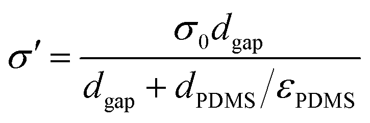
The effective contact between the triboelectric materials offers an opportunity for charge transfer, while the transferred charge density determines the output performance of TENGs. According to previous reports,16,19 the dielectric constant of the triboelectric material plays an important role in enhancing the charge density. The maximum transferred charge density (σ′) can be expressed as follows:16
 | (1) |
CaCu3Ti4O12 was intensively studied in recent years due to its unusually high dielectric constant.27,31,32 Herein, CaCu3Ti4O12 powder was prepared for enhancing the dielectric properties of the PDMS-based film. A common dielectric material BaTiO3 was also prepared for comparison. The XRD patterns of BTO and CCTO (Fig. 1e) indicate that the prepared particles are pure phase. The XRD peak splitting at 2θ = ∼45° (Fig. S4a†) and Raman spectrum of BTO (Fig. S4b†) suggest that BTO has a tetragonal phase.33 The BTO nanoparticles exhibit a rounded shape with sizes of 60–100 nm (Fig. S5a†). Besides, the TEM images of BTO nanoparticles (Fig. 1f) show that the distance of lattice strips is 1.8 Å, corresponding to the (210) plane of the tetragonal phase BTO. The morphology of CCTO particles is not uniform (Fig. S5b†). However, the lattice planes of CCTO are clearly visible with a d-spacing of 2.61 Å (Fig. 1g), which can be indexed to the (220) plane.
Fig. 2a depicts the dielectric constant of the PDMS-based composite films as a function of the BTO and CCTO contents (in weight percent). Obviously, the composite films exhibit a higher dielectric constant compared with the pure PDMS. The dielectric constant of the composite films increases almost linearly with the increment of the weight ratio of the embedded particles. In addition, when at the same weight ratio, the dielectric constant of PDMS–CCTO films is greater than those of PDMS–BTO films owing to the higher dielectric constant of CCTO.34 The enhanced dielectric constant may increase the transferred charge density; another parameter that can affect the output performance of TENGs is surface potential.16 It has been reported that there was a positive correlation between the surface charge potential of triboelectric materials and the output performance of the TENG.23 KPFM measurements were carried out to detect the surface potential of different surfaces (Fig. 2b). The average surface potential is −344.38 mV, 186.42 mV, 301.10 mV, and 448.30 mV for P(VDF-TrFE), PDMS, PDMS-30 wt% BTO (30BTO), and PDMS-30 wt% CCTO (30CCTO), respectively. Compared to the Pt-coated Si tip, the surface potential of the P(VDF-TrFE) film is negative. This may be caused by the intrinsic negative charges from the downward self-aligned region of dipoles in the spin-coated P(VDF-TrFE) thin film.35,36 The surface charge potential of PDMS is significantly enhanced after it was embedded with dielectric particles. The P(VDF-TrFE) and 30CCTO films have the largest surface potential difference, revealing better charge attracting properties.23
 | ||
| Fig. 2 (a) Dielectric constant of the composite films with different weight ratios. (b) KPFM images of the P(VDF-TrFE), PDMS, 30BTO and 30CCTO films, respectively. | ||
To further investigate the effects of surface morphology and embedded dielectric particles on the surface potential distribution of different triboelectric pairs, we performed COMSOL Multiphysics simulations. The same dimensions of triboelectric layers and gap distance were set in the simulation. Compared with the flat surface, the micro/nano-pattern increased the contact area of the two friction layers. Therefore, the patterned PDMS-based TENG exhibited a higher triboelectric potential (Fig. 3a and b).37 For contact-mode TENGs, the generated electric potential (VP) can be derived using: VP = σ′dgap/ε0, where ε0 is the vacuum permittivity.38,39 According to Fig. 2a and eqn (1), the transferred charge density σ′ of PDMS could be enhanced with the BTO and CCTO particles. Hence a higher triboelectric potential was obtained from the 30BTO-based TENG (Fig. 3c) and the 30CCTO-based TENG (Fig. 3d). The detailed surface potential difference of the PDMS-based films is shown in Fig. S6.†
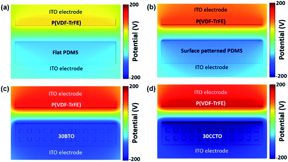 | ||
| Fig. 3 COMSOL simulation results for different triboelectric pairs. | ||
On the basis of the above results, the dielectric properties and surface potential of PDMS could be significantly enhanced with the embedded dielectric particles. Next, we investigated the electrical output performance of the TENGs. Flat PDMS, PDMS with an FTO patterned structure (FTO PDMS), BTO and CCTO embedded PDMS with an FTO patterned structure were fabricated. All of the as-prepared composite films have a thickness of ∼150 μm. The friction area was tailored to be 2.5 × 2.5 cm2. The voltage output of different triboelectric pairs is shown in Fig. S7.† The output voltage increased with the introduction of surface patterns and further increased with the addition of BTO nanoparticles (Fig. S7a†). However, the voltage value did not increase monotonically with increasing weight ratio of BTO, which dropped at 40 wt%. The voltage output of the PDMS–CCTO composite-based TENG exhibited a similar trend (Fig. S7b†). Although the embedded dielectric particles enhanced the surface charge density of PDMS, these particles also appeared on the surface of composite films (Fig. S8†), resulting in a reduction in the effective friction area of PDMS. Therefore, the optimal weight ratio (30%) is the competitive balance of the two impacts.
For better comparison, the output voltage, current density, and charge density of the PDMS-based TENG and TENGs based on PDMS-based composite films with the optimal weight ratio are shown in Fig. 4a–c. Evidently, the electric performance was enhanced with the introduction of surface patterns and dielectric particles. The 30CCTO-based TENG produced the highest values of voltage (∼390 V (peak to peak)), current density (∼170 mA m−2), and charge density (∼108 μC m−2), which were 5, 12, and 4 times higher than those of a flat PDMS-based TENG under the same measurement conditions, respectively. Additionally, different loaded resistors were inserted in the circuit to find the optimal output power of the TENGs. The voltage and current output of the 30CCTO-based TENG with different load resistances is presented in Fig. 4d. The other TENGs showed a similar trend (Fig. S9†), that is the voltage increased and current decreased with increasing load resistance. Accordingly, the resistance-dependent power density was calculated (Fig. 4e). A maximum power density of 9.6 W m−2 was obtained from the 30CCTO-based TENG, which is 10 times higher than that of a flat PDMS-based TENG. Furthermore, the capacitor charging characteristic of the TENGs was evaluated. The TENGs were integrated with a rectifying bridge circuit and a commercial capacitor (3.3 μF, 50 V). According to the recorded charging curves (Fig. 4f), the 30CCTO-based TENG took the shortest time for charging the capacitor to 50 V, indicating the most efficient energy harvesting behavior of the 30CCTO-based TENG. The stored electrical energy was capable of lighting 23 red LEDs (inset of Fig. 4f).
 | ||
| Fig. 4 Electrical output performance of the TENGs. (a–c) Voltage output, current density, and charge density of the TENGs, respectively. (d) Output voltage and current of the 30CCTO-based TENG according to the external load resistance. (e) The calculated power density values of the TENGs at different loaded resistances. (f) The charging properties of the TENGs; inset: LEDs lit using the capacitor charged using the 30CCTO-based TENG. | ||
The 30CCTO-based TENG can also act as power source for practical applications, and the basic schematic diagram of the circuit is illustrated in Fig. 5a. The alternating current generated from the TENG was converted to direct current firstly, and then used to charge a 47 μF capacitor. After a short while (within 45 s), the generated power could drive an electronic calculator continuously (Fig. 5b, ESI Video S1†). Besides, 23 red LEDs in series were connected to the 30CCTO-based TENG directly (without using the capacitor and rectifying bridge unit), the LEDs could be lit synchronously with hand tapping going on (Fig. 5c, ESI Video S2†). Moreover, based on the circuit shown in Fig. 5a, when placed in an energy harvesting module, the 30CCTO-based TENG could even charge a digital watch (Fig. 5d, ESI Video S3†). Finally, the stability is of great importance for a practical nanogenerator. The output voltage generated by the 30CCTO-based TENG did not appear to change obviously after a 10000 cycle test (Fig. 5e), revealing the excellent stability and durability of the TENG.
 | ||
| Fig. 5 (a) Basic circuit diagram of TENG application. (b) The photograph of an electronic calculator continuously driven by the 30CCTO-based TENG. (c) The photograph of 23 red LEDs directly lit by the 30CCTO-based TENG. (d) The photograph of the 30CCTO-based TENG charging a digital watch without any external energy sources. (e) Stability and durability tests of the 30CCTO-based TENG over 10000 cycles. | ||
Conclusions
In summary, we demonstrated a facile approach to improve the electric output performance of TENGs by the introduction of surface patterns and high dielectric particles. The surface potential of PDMS was dramatically enhanced with high dielectric particles, which has been supported by KPFM measurement and COMSOL Multiphysics simulations. With a combination of surface modification and dielectric constant control, the 30CCTO-based TENG produced a highest output power density of 9.6 W m−2, showing a 10-fold power enhancement in comparison with a flat PDMS-based TENG. The charging properties were also significantly enhanced. Moreover, the TENG showed excellent stability and could be used as a power supply for electronic calculators, commercial red LEDs, and digital watches. The demonstrated techniques provide a promising strategy for exploring high performance triboelectric generators.Conflicts of interest
There are no conflicts to declare.Acknowledgements
This work is supported by the National Research Foundation Singapore, Ministry of National Development, R-263-000-C22-277.Notes and references
- S. Chu and A. Majumdar, Nature, 2012, 488, 294 CrossRef CAS PubMed.
- Z. Song and H. Zhou, Energy Environ. Sci., 2013, 6, 2280 CAS.
- D. Larcher and J. Tarascon, Nat. Chem., 2015, 7, 19 CrossRef CAS PubMed.
- X. Cao, Y. Jie, N. Wang and Z. L. Wang, Adv. Energy Mater., 2016, 6, 1600665 CrossRef.
- Z. L. Wang, ACS Nano, 2013, 7, 9533 CrossRef CAS PubMed.
- S. H. Wang, X. J. Mu, Y. Yang, C. L. Sun, A. Y. Gu and Z. L. Wang, Adv. Mater., 2015, 27, 240 CrossRef CAS PubMed.
- L. Zhang, B. B. Zhang, J. Chen, L. Jin, W. L. Deng, J. F. Tang, H. T. Zhang, H. Pan, M. B. Zhu, W. Q. Yang and Z. L. Wang, Adv. Mater., 2016, 28, 1650 CrossRef CAS PubMed.
- W. Seung, M. K. Gupta, K. Y. Lee, K.-S. Shin, J.-H. Lee, T. Y. Kim, S. Kim, J. Lin, J. H. Kim and S.-W. Kim, ACS Nano, 2015, 9, 3501 CrossRef CAS PubMed.
- J. Chen, Y. Huang, N. N. Zhang, H. Y. Zou, R. Y. Liu, C. Y. Tao, X. Fan and Z. L. Wang, Nat. Energy, 2016, 138, 1 Search PubMed.
- H. Y. Guo, Z. Wen, Y. L. Zi, M.-H. Yeh, J. Wang, L. P. Zhu, C. G. Hu and Z. L. Wang, Adv. Energy Mater., 2016, 6, 1501593 CrossRef.
- Z. L. Wang, T. Jiang and L. Xu, Nano Energy, 2017, 39, 9 CrossRef CAS.
- A. Ahmed, Z. Saadatnia, I. Hassan, Y. L. Zi, Y. Xi, X. He, J. Zu and Z. L. Wang, Adv. Energy Mater., 2016, 7, 1601705 CrossRef.
- S. M. Li, J. Wang, W. B. Peng, L. Lin, Y. L. Zi, S. H. Wang, G. Zhang and Z. L. Wang, Adv. Energy Mater., 2017, 7, 1602832 CrossRef.
- H. Y. Guo, J. Chen, M.-H. Yeh, X. Fan, Z. Wen, Z. L. Li, C. G. Hu and Z. L. Wang, ACS Nano, 2015, 9, 5577 CrossRef CAS PubMed.
- C. He, C. B. Han, G. Q. Gu, T. Jiang, B. D. Chen, Z. L. Gao and Z. L. Wang, Adv. Energy Mater., 2017, 1700644 CrossRef.
- J. W. Lee, H. J. Cho, J. Chun, K. N. Kim, S. Kim, C. W. Ahn, I. W. Kim, J.-Y. Kim, S.-W. Kim, C. Yang and J. M. Baik, Sci. Adv., 2017, 3, e1602902 CrossRef PubMed.
- J. Ha, J. Chung, S. M. Kim, J. H. Kim, S. Shin, J. Y. Park, S. Lee and J.-B. Kim, Nano Energy, 2017, 36, 126 CrossRef CAS.
- J.-H. Lee, R. Hinchet, T. Y. Kim, H. Ryu, W. Seung, H.-J. Yoon and S.-W. Kim, Adv. Mater., 2015, 27, 5553 CrossRef CAS PubMed.
- J. Chun, J. W. Kim, W.-S. Jung, C.-Y. Kang, S.-W. Kim, Z. L. Wang and J. M. Baik, Energy Environ. Sci., 2015, 8, 3006 CAS.
- Y. J. Fan, X. S. Meng, H. Y. Li, S. Y. Kuang, L. Zhang, Y. Wu, Z. L. Wang and G. Zhu, Adv. Mater., 2015, 29, 1603115 CrossRef PubMed.
- G. Q. Suo, Y. H. Yu, Z. Y. Zhang, S. F Wang, P. Zhao, J. Y. Li and X. D. Wang, ACS Appl. Mater. Interfaces, 2016, 8, 34335 CAS.
- J. Chen, H. Y. Guo, X. M. He, G. L. Liu, Y. Xi, H. F. Shi and C. G. Hu, ACS Appl. Mater. Interfaces, 2016, 8, 736 CAS.
- W. Seung, H.-J. Yoon, T. Y. Kim, H. Ryu, J. Kim, J.-H. Lee, J. H. Lee, S. Kim, Y. K. Park, Y. J. Park and S.-W. Kim, Adv. Energy Mater., 2017, 7, 1600988 CrossRef.
- X. Y. Chen, X. Pu, T. Jiang, A. F. Yu, L. Xu and Z. L. Wang, Adv. Funct. Mater., 2016, 27, 1603788 CrossRef.
- Y. Yang, H. Zhang, Z.-H. Lin, Y. S. Zhou, Q. Jing, Y. Su, J. Yang, J. Chen, C. Hu and Z. L. Wang, ACS Nano, 2013, 7, 9213 CrossRef CAS PubMed.
- M. Y. Shi, J. X. Zhang, H. T. Chen, M. D. Han, S. Gowda, Z. M. Su, B. Meng, X. L. Cheng and H. X. Zhang, ACS Nano, 2016, 10, 4083 CrossRef CAS PubMed.
- C. C. Homes, T. Vogt, S. M. Shapiro, S. Wakimoto and A. P. Ramirez, Science, 2001, 293, 673 CrossRef CAS PubMed.
- X. Z. Wang, B. Yang, J. Q. Liu and C. S. Yang, J. Mater. Chem. A, 2017, 5, 1176 CAS.
- K. Y. Lee, S. K. Kim, J.-H. Lee, D. Seol, M. K. Gupta, Y. Kim and S.-W. Kim, Adv. Funct. Mater., 2016, 26, 3067 CrossRef CAS.
- J. Kim, J. H. Lee, H. Ryu, J.-H. Lee, U. Khan, H. Kim, S. S. Kwak and S.-W. Kim, Adv. Funct. Mater., 2017, 27, 1700702 CrossRef.
- J. H. Clark, M. S. Dyer, R. G. Palgrave, C. P. Ireland, J. R. Darwent, J. B. Claridge and M. J. Rosseinsky, J. Am. Chem. Soc., 2011, 133, 1016 CrossRef CAS PubMed.
- R. Löhnert, H. Bartsch, R. Schmidt, B. Capraro and J. Töpfer, J. Am. Ceram. Soc., 2015, 98, 141 CrossRef.
- A. D. Li, C. Z. Ge, P. Lu, D. Wu, S. B. Xiong and N. B. Ming, Appl. Phys. Lett., 1997, 70, 1616 CrossRef CAS.
- L. Singh, U. S. Rai, K. D. Mandal, B. C. Sin, H. Lee, H. Chung and Y. Lee, Mater. Charact., 2014, 96, 54 CrossRef CAS.
- J. H. Yang, T. Ryu, Y. Lansac, Y. H. Jang and B. H. Lee, Org. Electron., 2016, 28, 67 CrossRef CAS.
- H. Choi, J. Hong and K. No, Appl. Phys. Lett., 2012, 101, 042904 CrossRef.
- D. Jang, Y. Kim, T. Y. Kim, K. Koh, U. Jeong and J. Cho, Nano Energy, 2016, 20, 283 CrossRef CAS.
- S. Niu, Y. S. Zhou, S. Wang, Y. Liu, L. Lin, Y. Bando and Z. L. Wang, Nano Energy, 2014, 8, 150 CrossRef CAS.
- J.-H. Lee, J. Kim, T. Y. Kim, M. S. A. Hossain, S.-W. Kim and J. H. Kim, J. Mater. Chem. A, 2016, 4, 7983 CAS.
Footnote |
| † Electronic supplementary information (ESI) available. See DOI: 10.1039/c7ta07696g |
| This journal is © The Royal Society of Chemistry 2018 |