
Solvent engineering for forming stonehenge-like PbI2 nano-structures towards efficient perovskite solar cells†
Yongguang
Tu
 ,
Jihuai
Wu
*,
Xin
He
,
Panfeng
Guo
,
Tongyue
Wu
,
Hui
Luo
,
Quanzhen
Liu
,
Kai
Wang
,
Jianming
Lin
,
Miaoliang
Huang
,
Yunfang
Huang
,
Zhang
Lan
and
Sizhong
Li
,
Jihuai
Wu
*,
Xin
He
,
Panfeng
Guo
,
Tongyue
Wu
,
Hui
Luo
,
Quanzhen
Liu
,
Kai
Wang
,
Jianming
Lin
,
Miaoliang
Huang
,
Yunfang
Huang
,
Zhang
Lan
and
Sizhong
Li
Engineering Research Center of Environment-Friendly Functional Materials, Ministry of Education, Institute of Materials Physical Chemistry, Huaqiao University, Xiamen 361021, China. E-mail: jhwu@hqu.edu.cn; Fax: +86 595 22692229
First published on 24th January 2017
Abstract
The organic–inorganic lead halide layer is a crucial factor in determining the photovoltaic performance of perovskite solar cells. Based on solvent engineering, we developed a three-step sequential coating method to prepare a high-quality CH3NH3PbI3 layer based on solvent (isopropanol) substitution. Stonehenge-like PbI2 nanostructures with controllable morphology and crystallinity were prepared by solvent substitution instead of the conventional annealing-treatment, affording several channels for CH3NH3I to penetrate into the PbI2 film due to volume expansion, and thus enabling the complete conversion from PbI2 to perovskite. In addition, the device exhibited high reproducibility by our method and achieved a high 17.78% power conversion efficiency under one-sun illumination. Furthermore, we optimized the production craft and successfully fabricated a uniform perovskite film (10 cm × 10 cm) via solvent substitution.
Introduction
In recent years, solar cells based on organic–inorganic lead halide perovskite were one of the most important developments in the field of solar energy due to their numerous advantages, including low cost, a facile preparation process, good stability and high power conversion efficiency (PCE)1–4 as well as organic–inorganic lead halide perovskite unique features such as broad and strong light absorption,5 longer carrier lifetimes,6 long charge carrier diffusion length,7,8 and low exciton binding energy.9 With research development on perovskite solar cells, the power conversion efficiency keeps increasing,7,10–15 from 3.8% in 2009 (ref. 10) to >20% now.16 This fast increment surpasses most expectations, leapfrogging every other solution-processed solar cell technology. More recently, an improved 22.1% PCE was certified by NREL (http://www.nrel.gov/ncpv/images/efficiency_chart.jpg).The photovoltaic performance of perovskite solar cells is closely related to the quality of organic–inorganic lead halide layer,15,17 and the organic–inorganic lead halide deposition is crucial for fabricating high-performance perovskite solar cells. The perovskite layer can be accomplished mainly using either a one-step coating18–20 or a sequential two-step coating process.21–24
Typically, in a sequential two-step deposition of CH3NH3PbI3 layer, N,N-dimethylformamide (DMF) and dimethyl sulfoxide (DMSO) mixed solution of PbI2 is first deposited onto a scaffold layer by spin-coating or vacuum evaporation, and is dried at 70–100 °C for several minutes to remove the mixed solvents (DMF/DMSO), resulting in a compact crystalline PbI2 layer introduced by lateral constrained growth on the scaffold. Subsequently, the resulting PbI2 layer undergoes an intercalation reaction with an anhydrous isopropanol (IPA) solution of CH3NH3I to form a perovskite CH3NH3PbI3 layer. However, the tight surface layer of PbI2 would hinder the permeation of CH3NH3I, lead to the incomplete conversion of PbI2 to CH3NH3PbI3 and induce a low reproducibility of perovskite solar cells.25,26 To achieve a complete conversion from PbI2 to CH3NH3PbI3, several strategies have been developed. Wu and co-workers reported26 an amorphous PbI2 film preparation using DMSO, a strong coordinating solvent, to inhibit PbI2 crystallization and enhance PbI2 conversion and reproducibility. Liu and his colleague reported27 a mesoporous PbI2 scaffold synthesis by a simple time-dependent nucleation and growth method, which showed a high conversion and almost no hysteresis. Moreover, a self-assembled porous PbI2 film was formed by incorporating a small amount of 4-tert-butylpyridine (4-TBP) into the precursor solutions,28 which significantly facilitated the CH3NH3PbI3 perovskite formation.
Herein, we developed a facile three-step sequential coating method to prepare a high-quality CH3NH3PbI3 layer based on solvent (isopropanol) substitution. The difference between the three-step sequential coating method with the two-step sequential coating (or deposition) method lies in the deposition of PbI2 film via solvent IPA substitution by us instead of a conventional anneal-treatment developed by others. First, the effects of IPA-substitution time on the PbI2 film morphology, crystallization, growth and device characteristics are discussed with regard to the three-step sequential deposition approach. Secondly, a unique Stonehenge-like PbI2 nanostructure was endowed with affluent channels that are convenient for inserting CH3NH3I and enhancing the complete conversion. As a result, the device achieved a high power conversion efficiency of 17.78% and exhibited high reproducibility. Furthermore, we successfully fabricated a uniform perovskite film based on a large substrate (10 cm × 10 cm) via the optimized three-step sequential deposition.
Results and discussion
Fig. 1a shows a schematic of the three-step sequential spin-coating approach for fabricating a CH3NH3PbI3 layer. In detail, a PbI2-dissolved DMF–DMSO solution was first spin-coated onto the TiO2 substrate; IPA solvent was loaded onto the substrate to substitute DMF–DMSO solvent and crystallize PbI2, and then a CH3NH3I-dissolved IPA solution was loaded onto the PbI2 coated substrate to form CH3NH3PbI3via an intercalation reaction. For two-step coating, a PbI2-dissolved DMF solution was first spin-coated onto the TiO2 substrate, dried and then a CH3NH3I-dissolved IPA solution was spin-coated onto the PbI2 coated substrate to form CH3NH3PbI3via an intercalation reaction. The difference between the three-step spin-coating with the two-step spin-coating is the deposition of the PbI2 film via solvent IPA substitution for the former instead of a conventional anneal-treatment process for the latter. | ||
| Fig. 1 Schematic (a) the three-step sequential spin-coating method. (b) The crystal growth of Stonehenge-like PbI2 and perovskite films. | ||
It is well known that DMSO and DMF have better solubility for PbI2 than IPA due to their strong polarity. When IPA is introduced onto the wet PbI2 film, DMF and DMSO molecules diffuse into the upper IPA solvent and IPA molecules diffuse into the lower film; this process is termed as solvent substitution. The solubility of PbI2 reduces, and the amorphous PbI2 begins to crystallize by supersaturation from which heterogeneous nucleation is obtained at the solid–liquid interface. This is known as the recrystallization process. Moreover, the growth of PbI2 nucleus can be fine-controlled by adjusting the loading time. The samples are termed as IPA-0s, IPA-5s, etc.Fig. 1b shows the schematic of crystal growth for PbI2 and perovskite films.
To inquire about the unique reaction dynamic process, we measured the surface morphologies of PbI2 films prepared by different approaches. Fig. 2 shows the top-view SEM images. Fig. 2a shows the PbI2 film prepared by conventional two-step sequential deposition and annealing treatment at 70 °C for several minutes to remove the mixed solvents (DMF/DMSO), and it can be seen that a compact and uniform layer is formed, and the grains with size of ca. 100 nm were closely packed. To probe the incipient morphology of wet PbI2 film, we employed a fast high-vacuum treatment on the wet film under ca. 8 × 10⁻⁴ pa vacuum for 1 h to extract the solvent, as shown in Fig. 2b. It can be seen that the morphology of PbI2 film is flat but with some heterogeneous cracks caused by rapid vaporization of solvent. DMF solvent more easily volatilizes than DMSO due to its higher vapor pressure and lower boiling point (boiling point: DMF: 153 °C, DMSO: 189 °C; vapor pressure (mmHg 20 °C) DMF: 2.7, DMSO: 0.42). The interaction between DMSO and Pb2+ is much stronger than that of DMF because the coordination ratios between Pb and the solvents are 1![[thin space (1/6-em)]](https://www.rsc.org/images/entities/char_2009.gif) :2 and 1:1 for DMSO and DMF, respectively. Therefore, DMF solvent volatilizes faster than DMSO solvent in the wet film. On the other hand, the volume ratio for DMF and DMSO in the mixed solvent was 4:1; in other words, there was more DMF than DMSO in the mixed solvent, and considering the solvent volatile speed and amount, this eventually leads to a plain PbI2 film.
:2 and 1:1 for DMSO and DMF, respectively. Therefore, DMF solvent volatilizes faster than DMSO solvent in the wet film. On the other hand, the volume ratio for DMF and DMSO in the mixed solvent was 4:1; in other words, there was more DMF than DMSO in the mixed solvent, and considering the solvent volatile speed and amount, this eventually leads to a plain PbI2 film.
 | ||
| Fig. 2 Top-view SEM images. (a) Annealing treatment on the PbI2 film. (b) High-vacuum treated PbI2 film. (C–l) IPA substitution PbI2 films. All the scale bars represent 500 nm. | ||
The top-view SEM images of the PbI2 films prepared by the three-step sequential spin-coating of IPA solvent substitution for different loading times were also measured, and the results are shown in Fig. 2c–l. When the IPA solvent was loaded onto the wet PbI2 film, the film changed its colour rapidly from light to bright yellow, as shown in Movie 1.† For the IPA-0s sample (Fig. 2c, i.e. IPA solvent substitution loading time 0 seconds), the incipient plain morphology disappeared and the characteristics of porosity emerged. This is also indicative of heterogeneous nucleation. When the loading time was extended from 5 to 40 s (Fig. 2d–g), the heterogeneous crystals gradually grew. After 40 s, the PbI2 film had a complete mesoporous structure from top (Fig. 2g). With increased loading time (Fig. 2h–l), the PbI2 film coverage gradually reduced and IPA may have fostered vertical growth instead of lateral growth.
In order to further validate the PbI2 growth along the Z-axis, we took the cross-view SEM images of PbI2 films prepared by different approaches. As shown in Fig. 3a, the PbI2 film prepared by annealing was compact and uniform from top to bottom with a thickness of ca. 200 nm.
 | ||
| Fig. 3 Cross-view SEM images of PbI2 films. (a) By annealing treatment; (b) by IPA substitution for 10 seconds; (c) by IPA substitution for 60 seconds; (c) by IPA substitution for 100 s. All the scale bars represent 500 nm. | ||
Although the sample of IPA-10s in Fig. 3b has markedly different morphology, the upper part shows a mesoporous structure with plenty of crevices and the lower part is compact, as is marked in the image. As the loading time increased, as shown in Fig. 3c and d, the crystal structure of the vertical growth was very evident, presenting a Stonehenge-like layer. The thickness of IPA substitution was ca. 350 nm, as a result of IPA substitution fostering the volume expansion of the PbI2 film, which offers numerous paths for the subsequent MAI insertion.
Fig. 4 shows the XRD patterns of PbI2 films prepared by the three-step coating of IPA substitution for different loading times. It can be seen that the peak at 12.6° increased rapidly with the extension of the loading time, corresponding to the (001) lattice plane of crystallized PbI2,26 the enhancement of the crystallinity implies the growth of PbI2 grain, which suggests that the crystallization of Stonehenge-like PbI2 films could be fine-adjusted by tuning the IPA loading time. As reported, the crystallized PbI2 undergoes an intercalation reaction with CH3NH3I efficiently as the ordered crystal structure already exists.26 However, highly crystallized PbI2 needs more time for the complete conversion, and a caveat, associated with such long conversion times, is that the perovskite dissolves in the CH3NH3I solution over longer periods and hampers the transformation.12,29 Therefore, appropriate crystallinity is required for the latter intercalation reaction.
 | ||
| Fig. 4 XRD patterns of PbI2 films prepared by IPA substitution at different loading times. | ||
The subtle change in the early stage was further analyzed. The peak at 10° shows the existence of PbI2·xDMSO complexes30,31 in the samples of high-vacuum treatment and IPA-0s (as shown in Fig. S1†), while this peak was obscure in the sample of IPA-5s, indicating that the process of the IPA substitution was very quick.
We further monitored the dynamics of the Stonehenge-like PbI2 film by optical absorption. Fig. S2† gives the UV-Vis absorption spectra of the PbI2 films prepared by different approaches. The additional increase in the absorbance indicated that the light scattering was enhanced with the loading time from 0 to 60 s, which is ascribed to morphological changes of Stonehenge-like PbI2 film. From 60 to 120 s, the absorption spectra showed a dramatic decreasing trend that was consistent with the morphology and vertical growth. Pictures of PbI2 films prepared by annealing treatment and isopropanol substitution for 60 s are shown in Fig. S3.† There is a big difference in color between the two samples.
We fabricated the perovskite solar cells based on different types of PbI2 films. Detailed fabrication processes are described in the experimental section. In the experiment, we prepared the perovskite film by loading the MAI solution onto the Stonehenge-like PbI2 film, and the film immediately changed its color from yellow to dark brown, indicating the formation of perovskite CH3NH3PbI3. In our case, the Stonehenge-like PbI2 film with controllable crystallinity, which greatly enhanced the reaction kinetics, finally enabled the transformation to be completed within seconds.
The top-view SEM image of CH3NH3PbI3 film is shown in Fig. S4a.† As confirmed by the SEM images, the CH3NH3PbI3 film was compact and pinhole-free with cuboid sizes ranging from 200 to 600 nm that benefitted from the Ostwald ripening process.32–34 Fig. S5† shows the macroscopic morphologies of CH3NH3PbI3 films prepared by a three-step sequential spin-coating method, revealing a smooth film.
Fig. 5 shows the XRD patterns of CH3NH3PbI3 films prepared by different approaches. It can be seen that compared to the two-step annealing treatment, the CH3NH3PbI3 films fabricated from the three-step spin-coating of IPA substitution showed a reduced residue of PbI2, and when the loading time was extended from 20 to 80 s, there was no peak of PbI2 in the high-quality CH3NH3PbI3 film, indicating higher conversion ratio from PbI2 to CH3NH3PbI3 for the three-step coating than that of the two-step spin-coating.
 | ||
| Fig. 5 XRD patterns of CH3NH3PbI3 films prepared by different approaches. | ||
The CH3NH3PbI3 layer not only plays the role of a light absorber, but it is also the medium for charge transport, which directly depends on the film-quality and will have crucial influence on the device performance.35 Steady-state photoluminescence (PL) spectra and time resolved photoluminescence (TRPL) intensity decay measurements of CH3NH3PbI3 perovskite films can be used to explore the charge carrier extraction at the interface between the TiO2 and perovskite layers, and the samples were composed of FTO/CL-TiO2/mp-TiO2/perovskite. The steady-state PL spectra are shown in Fig. 6a. The steady-state PL intensity of IPA-20 was greatly quenched, indicating that there was an effective charge transfer from perovskite to TiO2. However, residual PbI2 in the interface of TiO2/perovskite may block the charge transportation because of its higher conduction band over perovskite.36 The PL intensity of the different perovskite films was consistent with the residue of PbI2. Fig. 6b shows the time resolved photoluminescence (TRPL) intensity decay, and the curves were fitted with a two exponential decay function and the corresponding lifetimes were obtained, as listed in Table S1.† The charge carrier lifetimes (τ) were 23.24 ns, 18.13 ns, 10.32 ns, 9.66 ns, and 13.79 ns, corresponding to the samples annealed, IPA-5s, IPA-20s, IPA-60s, and IPA-100s, respectively. The shorter τ value indicates that the charge transfer from the perovskite to TiO2 layer was faster.
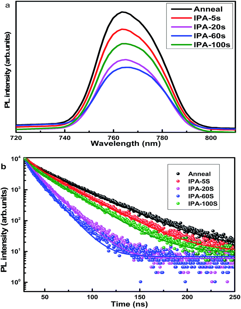 | ||
| Fig. 6 (a) Steady state photoluminescence spectra detected at peak 460 nm excitation wavelength; (b) time-resolved photoluminescence intensity decay of CH3NH3PbI3 detected at peak emission wavelength of 764 nm. | ||
The perovskite solar cells were fabricated using CH3NH3PbI3 from different preparation methods. The photocurrent–voltage (J–V) curves of the devices were measured under AM 1.5G (100 mW cm−2), which is shown in Fig. 7 and the corresponding photovoltaic parameters are listed in Table 1. For the device with CH3NH3PbI3 prepared by the two-step sequential deposition, a PCE of 14.55% was achieved with short-circuit current density (JSC) of 21.44 mA cm−2, open-circuit photovoltage (VOC) of 1.013 V and fill factor (FF) of 0.67. For the devices with CH3NH3PbI3 prepared by the three-step sequential coating method with IPA substitution, the performance increased with an increase in the loading time from 0 to 60 s. The perovskite solar cell prepared by the three-step sequential coating of IPA solvent substitution for 60 s achieved the highest PCE value of 17.78% and a JSC of 22.35 mA cm−2, VOC of 1.075 V and FF of 0.74. The increased FF and VOC suggest that more PbI2 was transformed into CH3NH3PbI3, which are substantiated by the XRD patterns of CH3NH3PbI3 films prepared by different approaches (as shown in Fig. 5a and b). With further extending the loading time, the performance began to decline. Appropriate morphology and crystallization of Stonehenge-like PbI2 films is the key to obtaining higher efficiency.
 | ||
| Fig. 7 J–V curves of the PSCs based on different PbI2 under AM 1.5G illumination. | ||
| Samples | V OC (V) | J SC (mA cm−2) | FF | PCE (%) |
|---|---|---|---|---|
| Annealing treatment | 1.013 | 21.44 | 0.67 | 14.55 |
| IPA-0s | 1.002 | 18.42 | 0.65 | 11.99 |
| IPA-5s | 1.036 | 20.34 | 0.67 | 14.11 |
| IPA-10s | 1.049 | 21.26 | 0.69 | 15.38 |
| IPA-20s | 1.064 | 21.90 | 0.72 | 16.77 |
| IPA-40s | 1.073 | 22.04 | 0.73 | 17.26 |
| IPA-60s | 1.075 | 22.35 | 0.74 | 17.78 |
| IPA-80s | 1.062 | 22.04 | 0.70 | 16.38 |
| IPA-100s | 1.054 | 22.09 | 0.67 | 15.60 |
| IPA-120s | 1.018 | 19.75 | 0.65 | 13.07 |
| IPA-150s | 0.996 | 17.46 | 0.56 | 9.74 |
It is well known that the notorious photocurrent density–voltage (J–V) hysteresis often exists in perovskite solar cells when measured under different scan directions, which makes accurate efficiency determination challenging.37 Fig. S6† shows the J–V curve of the best device under both reverse and forward bias scans, and that there is a hysteresis effect. For the reverse scan, the device shows a 17.78% power conversion efficiency (PCE) with a 1.075 V open-circuit voltage (VOC), 22.35 mA cm−2 short-circuit current density (JSC), and 0.74 fill factor (FF). For the forward scan, the device shows a PCE of 13.58% with VOC of 1.029 V, JSC of 22.36 mA cm−2, and FF of 0.59.
Fig. 8 shows the incident-photon-to-current conversion efficiency (IPCE) for the perovskite solar cell fabricated by three-step sequential coating of IPA solvent substitution for 60 s. IPCE reached peak values over 90% in the short-wavelength region of the visible spectrum. The integrated JSC was calculated to be 21.99 mA cm−2, which is close to the measured JSC of 22.35 mA cm−2. This confirms that any mismatch between the simulated sunlight and the AM 1.5G standard was negligibly small.12 Fig. S7† shows the steady-state photocurrent and output PCE of the devices in the IPA-60s group at the maximum power points with a stabilized current density output of 19.25 mA cm−2 (at a voltage of 0.88 V), yielding a PCE of 16.92%.
 | ||
| Fig. 8 IPCE spectrum (black line) and integrated photocurrent density JSC (red line) for the champion cell. | ||
Statistical results of the cell performance are provided in Fig. S8† in the form of histogram charts. It can be seen that the devices based on IPA-60s showed better performance and the average PCE was 17.12%. Moreover, the histogram chart demonstrated high reproducibility of the devices from IPA substitution (each group was calculated from a batch of 50 cells).
For future applications, the spin-coating method was not compatible with large-scale production processes. Herein, we further optimized the production craft and reduced spin-coating process towards up-scaling. Specifically, the resulting TiO2/PbI2 film (10 cm × 10 cm) was dipped into the IPA solvent for 60 s for solvent substitution; after 60 s, the film was dipped into the CH3NH3I-dissolved IPA solution for 60 s in order to prepare the perovskite layer. The resulting perovskite film was washed with IPA and heated at 70 °C for 5 min and 100 °C for 30 min. As show in Movie 1,† when the wet resulting PbI2 film (10 cm × 10 cm) was dipped into the IPA solvent, the film changed its color from light to bright yellow rapidly. Fig. 9 shows the pictures of the PbI2 film and CH3NH3PbI3 films (10 cm × 10 cm). A uniform PbI2 layer was obtained by spin-coating, as shown in Fig. 9a. Fig. 9b–c show perovskite film by IPA substitution, presenting an even dark red brown.
 | ||
| Fig. 9 Photographs of PbI2 film and CH3NH3PbI3 films (10 cm × 10 cm) prepared by IPA substitution. (a) PbI2 film prepared by IPA substitution (10 cm × 10 cm); (b) and (c) CH3NH3PbI3 films (10 cm × 10 cm). | ||
Conclusion
In conclusion, we established a facile three-step sequential coating method to prepare a high-quality CH3NH3PbI3 layer based on solvent (isopropanol) substitution instead of routine annealing treatments. Isopropanol (IPA) solvent substitution had a significant impact on the crystallinity and porosity of PbI2 films, which is beneficial for the conversion of PbI2 to CH3NH3PbI3. The three-step sequential coating method can reduce PbI2 residue and enhance the reproducibility of the performance of the device. The perovskite solar cell with CH3NH3PbI3 fabricated by the three-step sequential coating of IPA solvent substitution achieved a high power conversion efficiency of 17.78% under one-sun illumination. Under the same condition, the device with CH3NH3PbI3 fabricated by the two-step sequential deposition of anneal-treatment obtained a power conversion efficiency of 14.55%. Furthermore, we successfully fabricated a uniform perovskite film based on a large substrate (10 cm × 10 cm) via an optimized three-step sequential deposition. These results provide important progress towards the understanding of the role of solution engineering in the realization of up-scaling and highly efficient perovskite solar cells.Methods
Materials and reagents
All of the materials were purchased from the Sigma-Aldrich Corp. if not specified. The spiro-OMeTAD was from Merk. CH3NH3I was synthesized according to a literature method.38Device fabrication
Fluorine-doped tin oxide-coated (FTO) glass (Pilkington, TEC-8, 8 Ω per sq) was cleaned by UV-ozone treatment for 15 min, followed by consecutive cleaning with detergent and ethanol. The compact TiO2 blocking layers were deposited onto an FTO glass, which was prepared by spin-coating 0.15 M titanium diisopropoxide bis(acetylacetonate) (75 wt% in isopropanol, Aldrich) in 1-butanol (99.8%, Aldrich) solution, at 500 rpm for 5 seconds and 2000 rpm for 30 s and then dried at 125 °C for 5 min. A mesoporous TiO2 film was deposited on a compact TiO2 layer by spin-coating TiO2 paste diluted in ethanol. TiO2 paste was prepared as described previously.3,17,39,40 After drying at 100 °C for 5 min, the film was annealed at 450 °C for 30 min, providing a thickness of ca. 150 nm. The mesoporous TiO2 film was immersed in 0.02 M aqueous TiCl4 solution at 90 °C for 10 min. After washing with deionized water and alcohol, the film was heated at 500 °C for 30 min.CH3NH3PbI3 layer was prepared using a three-step sequential spin-coating approach. PbI2 solution (1 M) was prepared by dissolving in a mixture of DMF and DMSO (4:1 v/v) at 70 °C. PbI2 solution (20 µL) was spin-coated on the mesoporous TiO2 film at 6000 rpm for 15 s. Moreover, 200 µL isopropanol was loaded onto the PbI2 film for different times, which was spun at 4000 rpm for 30 s. Then, a 200 µL of 20 mg mL−1 CH3NH3I solution in isopropanol was loaded onto the former film for 60 s (loading time), which was spun at 4000 rpm for 20 s and dried at 70 °C for 5 min and 100 °C for 30 min.
A volume of 20 µL of 2,2′,7,7′-tetrakis(N,N-di-p-methoxyphenylamine)-9,9-spirobifluorene (spiro-OMeTAD) solution was spin-coated onto the CH3NH3PbI3 perovskite layer at 4000 rpm for 30 s. A spiro-OMeTAD solution was prepared by dissolving 72.3 mg of spiro-OMeTAD in 1 mL of chlorobenzene, to which 28.8 µL of 4-tert-butyl pyridine and 17.5 µL of lithium bis(trifluoromethanesulfonyl)imide (Li-TFSI) solution (520 mg LI-TSFI in 1 mL acetonitrile, Sigma-Aldrich, 99.8%) were added. All devices were stored in a desiccator (humidity < 15%) in the dark for 12 h. Finally, 80 nm of gold was deposited under vacuum through a shadow mask.
Characterization
The current density–voltage (J–V) curves were measured using a Keithley 2420 source-measure unit under AM1.5G illumination at 100 mW cm−2 provided by an Oriel Sol 3A solar simulator in ambient environment. The light intensity was adjusted using a NREL-calibrated Si solar cell equipped with KG-2 filter. The devices had an active area of 0.125 cm2 without the metal mask. The devices were measured by reverse (2.0 to −0.1 V) and forward (−0.1 to 2.0 V) voltage scanning at about a 21.2 mV scan step (100 data points in total). The pre-sweep delay time was 40 ms and the dwell time at each voltage step was 30 ms. Surface morphologies were characterized by field-emission scanning electron microscopy (SEM, Hitachi S-8000, Japan). The crystalline structures were examined using X-ray diffraction (XRD, Bruker AXS, D8 Advance). IPCE curves were measured as a function of wavelength from 300 nm to 800 nm using the Newport IPCE system (Newport, USA). The time-resolved photoluminescence spectrum was acquired using the time-correlated single-photon counting technique (Pico harp 300), and the excitation light pulse was provided using a picosecond diode laser at a 760 nm wavelength with a 1 MHz repetition frequency (PDL 800B).Author contributions
J. W. conceived the project, J. W. and Y. T. designed the device and experiments, and Y. T. carried out most of the experiments. Y. T. wrote the first draft of the manuscript, and J. W. finished the submitted paper. All the authors discussed the results and approved of publishing this paper.Acknowledgements
The authors acknowledge the financial joint support by the National Natural Science Foundation of China (No. 91422301, 51472094, 61474047, 21301060, 61306077, U1205112), and the Cultivation Program for Postgraduate in Scientific Research Innovation Ability of Huaqiao University (No. 1400102002).References
- G. Hodes, Science, 2013, 342, 317–318 CrossRef CAS PubMed.
- R. F. Service, Science, 2014, 344, 458 CrossRef PubMed.
- J. Wu, Z. Lan, J. Lin, M. Huang, Y. Huang, L. Fan and G. Luo, Chem. Rev., 2015, 115, 2136–2173 CrossRef CAS PubMed.
- W. Chen, Y. Wu, Y. Yue, J. Liu, W. Zhang, X. Yang, H. Chen, E. Bi, I. Ashraful, M. Grätzel and L. Han, Science, 2015, 350, 944–948 CrossRef CAS PubMed.
- Z. Xiao, C. Bi, Y. Shao, Q. Dong, Q. Wang, Y. Yuan, C. Wang, Y. Gao and J. Huang, Energy Environ. Sci., 2014, 7, 2619–2623 CAS.
- C. Wehrenfennig, G. E. Eperon, M. B. Johnston, H. J. Snaith and L. M. Herz, Adv. Mater., 2014, 26, 1584–1589 CrossRef CAS PubMed.
- S. D. Stranks, G. E. Eperon, G. Grancini, C. Menelaou, M. J. Alcocer, T. Leijtens, L. M. Herz, A. Petrozza and H. J. Snaith, Science, 2013, 342, 341–344 CrossRef CAS PubMed.
- G. Xing, N. Mathews, S. Sun, S. S. Lim, Y. M. Lam, M. Grätzel, S. Mhaisalkar and T. C. Sum, Science, 2013, 342, 344–347 CrossRef CAS PubMed.
- V. D'Innocenzo, G. Grancini, M. J. Alcocer, A. R. Kandada, S. D. Stranks, M. M. Lee, G. Lanzani, H. J. Snaith and A. Petrozza, Nat. Commun., 2014, 5, 3586 Search PubMed.
- A. Kojima, K. Teshima, Y. Shirai and T. Miyasaka, J. Am. Chem. Soc., 2009, 131, 6050–6051 CrossRef CAS PubMed.
- M. M. Lee, J. Teuscher, T. Miyasaka, T. N. Murakami and H. J. Snaith, Science, 2012, 338, 643–647 CrossRef CAS PubMed.
- J. Burschka, N. Pellet, S. J. Moon, R. Humphry-Baker, P. Gao, M. K. Nazeeruddin and M. Grätzel, Nature, 2013, 499, 316–319 CrossRef CAS PubMed.
- M. Liu, M. B. Johnston and H. J. Snaith, Nature, 2013, 501, 395–398 CrossRef CAS PubMed.
- H. Zhou, Q. Chen, G. Li, S. Luo, T. B. Song, H. S. Duan, Z. Hong, J. You, Y. Liu and Y. Yang, Science, 2014, 345, 542–546 CrossRef CAS PubMed.
- W. S. Yang, J. H. Noh, N. J. Jeon, Y. C. Kim, S. Ryu, J. Seo and S. I. Seok, Science, 2015, 348, 1234–1238 CrossRef CAS PubMed.
- D. Bi, W. Tress, M. I. Dar, P. Gao, J. Luo, C. Renevier, K. Schenk, A. Abate, F. Giordano, J. C. Baena, J. Decoppeet, S. M. Zakeeruddin, M. K. Nazeeruddin, M. Grätzel and A. Hagfeldt, Sci. Adv., 2016, 2, e1501170 Search PubMed.
- Y. Tu, J. Wu, M. Zheng, J. Huo, P. Zhou, Z. Lan, J. Lin and M. Huang, Nanoscale, 2015, 7, 20539–20546 RSC.
- M. Xiao, F. Huang, W. Huang, Y. Dkhissi, Y. Zhu, J. Etheridge, A. Gray-Weale, U. Bach, Y. B. Cheng and L. Spiccia, Angew. Chem., Int. Ed., 2014, 53, 9898–9903 CrossRef CAS PubMed.
- N. J. Jeon, J. H. Noh, Y. C. Kim, W. S. Yang, S. Ryu and S. I. Seok, Nat. Mater., 2014, 13, 897–903 CrossRef CAS PubMed.
- N. Ahn, D. Y. Son, I. H. Jang, S. M. Kang, M. Choi and N. G. Park, J. Am. Chem. Soc., 2015, 137, 8696–8699 CrossRef CAS PubMed.
- C.-G. Wu, C.-H. Chiang, Z.-L. Tseng, M. K. Nazeeruddin, A. Hagfeldt and M. Grätzel, Energy Environ. Sci., 2015, 8, 2725–2733 CAS.
- Y. Xiao, G. Han, Y. Li, M. Li and Y. Chang, J. Mater. Chem. A, 2014, 2, 16531–16537 CAS.
- D. Yang, Z. Yang, W. Qin, Y. Zhang, S. Liu and C. Li, J. Mater. Chem. A, 2015, 3, 9401–9405 CAS.
- Z. Yang, B. Cai, B. Zhou, T. Yao, W. Yu, S. Liu, W.-H. Zhang and C. Li, Nano Energy, 2015, 15, 670–678 CrossRef CAS.
- T. Zhang, M. Yang, Y. Zhao and K. Zhu, Nano Lett., 2015, 15, 3959–3963 CrossRef CAS PubMed.
- Y. Wu, A. Islam, X. Yang, C. Qin, J. Liu, K. Zhang, W. Peng and L. Han, Energy Environ. Sci., 2014, 7, 2934–2938 CAS.
- T. Liu, Q. Hu, J. Wu, K. Chen, L. Zhao, F. Liu, C. Wang, H. Lu, S. Jia, T. Russell, R. Zhu and Q. Gong, Adv. Energy Mater., 2015, 1501890 Search PubMed.
- H. Zhang, J. Mao, H. He, D. Zhang, H. L. Zhu, F. Xie, K. S. Wong, M. Grätzel and W. C. H. Choy, Adv. Energy Mater., 2015, 1501354 CrossRef.
- K. Liang, D. Mitzi and M. Prikas, Chem. Mater., 1998, 10, 403–411 CrossRef CAS.
- S. Bae, S. Han, T. Shin and W. Jo, J. Mater. Chem. A, 2015, 3, 23964–23972 CAS.
- Y. Zou and R. Holmes, Adv. Energy Mater., 2016, 1501994 CrossRef.
- M. Yang, T. Zhang, P. Schulz, Z. Li, G. Li, D. H. Kim, N. Guo, J. J. Berry, K. Zhu and Y. Zhao, Nat. Commun., 2016, 7, 12305 CrossRef CAS PubMed.
- W. Zhu, C. Bao, Y. Wang, F. Li, X. Zhou, J. Yang, B. Lv, X. Wang, T. Yu and Z. Zou, Dalton Trans., 2016, 45, 7856–7865 RSC.
- N. Sakai, S. Pathak, H.-W. Chen, A. A. Haghighirad, S. D. Stranks, T. Miyasaka and H. J. Snaith, J. Mater. Chem. A, 2016, 4, 4464–4471 CAS.
- J. W. Lee, D. J. Seol, A. N. Cho and N. G. Park, Adv. Mater., 2014, 26, 4991–4998 CrossRef CAS PubMed.
- F. Zhang, C. Yi, P. Wei, X. Bi, J. Luo, G. Jacopin, S. Wang, X. Li, Y. Xiao, S. M. Zakeeruddin and M. Grätzel, Adv. Energy Mater., 2016, 1600401 CrossRef.
- D. Yang, X. Zhou, R. Yang, Z. Yang, W. Yu, X. Wang, C. Li, S. Liu and R. P. H. Chang, Energy Environ. Sci., 2016, 9, 3071–3078 CAS.
- A. K. Chandiran, A. Yella, M. T. Mayer, P. Gao, M. K. Nazeeruddin and M. Grätzel, Adv. Mater., 2014, 26(25), 4309–4312 CrossRef CAS PubMed.
- J. Wu, S. Hao, Z. Lan, J. Lin, M. Huang, Y. Huang, P. Li, S. Yin and T. Sato, J. Am. Chem. Soc., 2008, 130, 11568–11569 CrossRef CAS PubMed.
- J. H. Wu, Z. Lan, J. M. Lin, M. L. Huang, S. C. Hao, T. Sato and S. Yin, Adv. Mater., 2007, 19(22), 4006–4011 CrossRef CAS.
Footnote |
| † Electronic supplementary information (ESI) available. See DOI: 10.1039/c6ta11004e |
| This journal is © The Royal Society of Chemistry 2017 |