
Few-layer MoS2 flakes as a hole-selective layer for solution-processed hybrid organic hydrogen-evolving photocathodes†
Sebastiano
Bellani‡
a,
Leyla
Najafi‡
ab,
Andrea
Capasso
a,
Antonio Esau
Del Rio Castillo
a,
Maria Rosa
Antognazza
 c and
Francesco
Bonaccorso
*a
c and
Francesco
Bonaccorso
*a
aGraphene Labs, Istituto Italiano di Tecnologia, via Morego 30, 16163 Genova, Italy. E-mail: francesco.bonaccorso@iit.it
bUniversità degli studi di Genova, Dipartimento di Chimica e Chimica Industriale, Via Dodecaneso 31, 16163 Genova, Italy
cCenter for Nano Science and Technology@Polimi, Istituto Italiano di Tecnologia, Via Pascoli 70/3, 20133 Milano, Italy
First published on 10th February 2017
Abstract
High-efficiency organic photocathodes, based on a regioregular poly(3-hexylthiophene) and phenyl-C61-butyric acid methyl ester (rr-P3HT:PCBM) bulk heterojunction sandwiched between charge-selective layers, are emerging as efficient and low-cost devices for solar hydrogen production by water splitting. Nevertheless, stability issues of the materials used as charge-selective layers are hampering the realization of long-lasting photoelectrodes, pointing out the need to investigate novel and stable materials. Here, we propose MoS2 flakes, produced by Li-aided exfoliation of the bulk counterpart, as an efficient atomic-thick hole-selective layer for rr-P3HT:PCBM-based photocathodes. We carried out p-type chemical doping to tune on-demand the MoS2 Fermi level in order to match the highest occupied molecular orbital level of the rr-P3HT, thus easing the hole collection at the electrode. The as-prepared p-doped MoS2-based photocathodes reached a photocurrent of 1.21 mA cm−2 at 0 V vs. RHE, a positive onset potential of 0.56 V vs. RHE and a power-saved figure of merit of 0.43%, showing a 6.1-fold increase with respect to pristine MoS2-based photocathodes, under simulated 1 sun illumination. Operational activity of the photocathodes over time and under 1 sun illumination revealed a progressive stabilization of the photocurrents at 0.49 mA cm−2 at 0 V vs. RHE. These results pave the way towards the exploitation of layered crystals as efficiency-boosters for scalable hybrid organic H2-evolving photoelectrochemical cells.
Introduction
Sunlight and water are the most abundant, clean and renewable energy resources.1 In fact, hydrogen (H2) fuel production via photoelectrochemical (PEC) water splitting (2H2O + hν → 4H2 + O2) represents one of the most challenging technologies for the production of clean carbon-neutral energy.2 The water splitting process consists of both reduction and oxidation half-reactions, i.e.: (i) oxygen evolution reaction (OER: 2H2O → O2 + 4H+ + 4e−) and (ii) hydrogen evolution reaction (HER: 4H+ + 4e− → 2H2).3 In general, a water splitting PEC cell comprises a semiconductor photoelectrode and a counter electrode immersed in an aqueous electrolyte.3–5 Semiconductor photoelectrodes absorb light photogenerating electrical charges, which are needed to carry out the redox chemistry of the OER and HER processes.3–5 For an n-type semiconductor electrode (photoanode),5 such as TiO2 (ref. 3,4) and α-Fe2O3,3 photoexcited holes are transferred to the semiconductor/electrolyte junction where they enable the OER,3 while electrons are transferred to the counter electrode where they allow the HER.3 Vice versa, in the case of a p-type semiconductor electrode (photocathode)5 such as p-Si,6 p-InP,7a and p-GaAs,7b HER and OER processes occur at the semiconductor/electrolyte junction and the counter electrode, respectively.3–5 The solar to hydrogen conversion efficiency (ηSTH) is the most important figure of merit (FoM) of a PCE cell and is defined as:where jsc is the short-circuit photocurrent density, ηF is the faradaic efficiency for hydrogen evolution, and P is the incident illumination power density, measured under standard solar illumination conditions (AM1.5G).8 This FoM directly depends on the photophysical properties of the semiconductor photoelectrodes, such as light absorption4,5 and exciton formation,8 as well as charge carrier separation and transport.8 The photogenerated electrons and holes have to overcome energetic constraints, corresponding to the thermodynamic potential of the HER and OER processes, respectively.4,5,8 In particular, the electrochemical potential of the bottom of the photoelectrode conduction band must be more negative than the H+/H2 redox level (

 ),3–5,8 while the one of the top of the valence band must be more positive than the O2/H2O redox level (
 ).3–8 Moreover, in view of scaling up and commercialization of PEC cells, stability and cost are also key factors.2,3 To date, extensive research on photoelectrodes for PEC cells has been focused on inorganic metal oxide/nitride such as TiO2,3,4,9 ZnO,10 WO3,11 α-Fe2O3,3,12 BiVO4,13 Ta2O5,14 TaON15 and Ta3N5,15 due to their energy band gap exceeding 1.23 eV,2–5,8–15 stability and Earth-abundance.2,3,8 Nevertheless, these single semiconductor absorbers cannot harvest a significant portion of the solar spectrum and therefore their potential ηSTH is intrinsically limited (predicted maximum values ∼ 13%).8–15 In order to overcome this problem, an ideal PEC cell based on a dual light absorber, or tandem configuration, can be used. A simple two-photoelectrode approach to construct a PEC cell for water splitting is to use an n-type semiconductor photoanode together with a p-type semiconductor photocathode.8,9 In this context, the vertical stacking of a 1.6–1.8 eV energy band gap semiconductor, such as InP,7 GaInP2,16 AlGaAs,17 Cu2O18 on top of a narrower (∼1 eV) one, such as Si,6,17,19 is emerging as a promising route to optimize the solar photon harvesting (photons not absorbed by the first material are transmitted to and absorbed by the second one).8,9,17,19 Recently, tandem water splitting using perovskite photovoltaics and CuInxGa1−xSe2 photocathodes20 or α-Fe2O3 photoanodes21 reached ηSTH of 6% and 2.4%, respectively. However, the instability in aqueous solutions of the photoactive semiconductors6,7,16–21 is their main drawback for long time operation. To overcome this issue, encapsulation strategies of the photoactive semiconductors have been proposed,18,22,23 with the result of increasing the overall fabrication costs. Thus, the discovery of new photoelectrode materials is needed to further improve the water splitting efficiency and long term stability with respect to the current technology.6,22 In the quest for the development of new photoelectrode materials, recently, organic semiconductors, such as graphitic carbon nitrides (g-C3N4),24 1,3,5-tris-(4-formyl-phenyl)triazine-based covalent organic frameworks (TFPT-COF),25a triarylamine-based microporous organic network (TAA-MON),25b hydrogen-bonded organic pigments of the epindolidione (EPI) and quinacridone (QNC),26a and boron subnaphthalocyanine chloride (SubPc):α-sexithiophene (6T) blend,26b have been exploited for the HER process. Sprick et al. reported conjugated microporous polymers (CMPs) based on a copolymer with varying ratios of benzene and pyrene as semiconductors for the HER with the optical band gap finely tuned over a broad range (i.e., 1.94–2.95 eV), thus making them versatile materials for tandem configurations.27 Finally, PEC electrodes for the HER based on semiconducting polymers (SPs) also emerged.28,29 These studies focused mainly on the use of regio regular poly(3-hexylthiophene) (rr-P3HT),28,29 the prototypical conjugated polymer widely used in bulk heterojunction (BHJ) organic photovoltaics (OPV) architectures,30 capable of delivering a record photocurrent density (under 1 sun illumination) of up to 14 mA cm−2.31 rr-P3HT has a direct bandgap of 1.9 eV,30,31 close to the optimum value for a PEC tandem device (maximum ηSTH of 21.6% is predicted for stacking 1.89 eV and 1.34 eV energy band gap semiconductors).8,9 The rr-P3HT lowest unoccupied molecular orbital (LUMO) energy level is several hundreds of millivolts more negative than the
  potential (LUMOP3HT –
  ∼ −1.5 V);30,31 thus photogenerated electrons possess the energy enabling the HER process.32 Moreover, the optoelectronic properties of rr-P3HT, such as light absorption and charge photogeneration, are fully retained in an aqueous environment.33 On the basis of these observations, rr-P3HT:phenyl-C61-butyric acid methyl ester (PCBM) BHJ-based photocathodes with photocurrent densities at the RHE potential (J0 V vs. RHE) in the mA cm−2 range have been reported.28,29,34 In these photocathodes, rr-P3HT:PCBM BHJ is sandwiched between two charge-selective layers (CSLs), resembling OPV architectures.35 Specifically, the hole-selective layer (HSL) is deposited between a transparent conductive oxide (TCO), e.g. indium tin oxide (ITO)32 or fluorine doped tin oxide (FTO),28,29,32 and the rr-P3HT:PCBM,28,29,32,34 while the electron-selective layer (ESL) is deposited on top of the rr-P3HT:PCBM.28,29 The device is completed by depositing an electrocatalyst (EC) for the HER, giving the overall structure TCO/HSL/rr-P3HT:PCBM/ESL/EC.28,29 The key role of the CSLs relies on the hole and electron transport28,29,35 toward TCO and EC, respectively. Once the electrons are collected in the EC, the HER process is activated.8,9,28,29 Currently, ZnO,28a,34 MoO3 (ref. 29a and b) and CuI29d are the most used HSLs, while TiO2 (ref. 28 and 29) and metallic Al/Ti29c are exploited as ESLs. Poly(3,4-ethylenedioxythiophene):poly(styrene sulfonate) (PEDOT:PSS),36 the typical HSL in OPV,37 poorly performed (J0 V vs. RHE in the sub mA cm−2 region) in perovskite solar cells (PSCs),29a due to ion penetration and electrochemical doping processes, which could alter its electrical properties.38 Amongst the ECs suitable for the HER process, both Pt28a–d,29b,d and metal-free catalysts, such as MoS3 (ref. 28d, 29a and c) and Chloro(pyridine)cobaloxime(III),34 have been exploited, turning out photocathodes with J0 V vs. RHE above 8 mA cm−2 and onset potential (Voc) (defined as the potential at which the photocurrent related to the HER is observed) of ∼0.7 V vs. RHE, a value similar to the open-circuit potential of the rr-P3HT:PCBM-based solar cell.30
Despite the continuous improvements, in terms of J0 V vs. RHE and Voc, stability issues of the rr-P3HT:PCBM-based photocathodes have been evidenced for the CSLs, under H2-evolving electrochemical conditions.28,29 For instance, irreversible electrochemical degradation of hygroscopic PEDOT:PSS28a,29c and water-soluble CuI,29d intercalation processes and irreversible reduction into sub-stoichiometric phases of MoO3 (ref. 29b) and WO3 (ref. 28a) with unfavourable energy alignment for their use as HSLs, led to the corresponding photocathodes' lifetimes during continuous operation ranging from several minutes to few hours.28a Consequently, most attention is now focused toward the discovery of new CSL materials, which could in principle boost the aforementioned photoelectrochemical FoMs.39 In this context, two dimensional (2D)-transition metal dichalcogenides (TMDs) are raising interest, due to their optoelectronic properties, for the integration as CSLs40 in heterojunction-based solar cells,41 both in OPV40,41,43 and inorganic photovoltaics (IPV).41,43,44 Amongst TMDs, MoS2 is in a key position due to its high charge carrier mobility (up to ≈470 cm2 V−1 s−1 for electrons, and ≈480 cm2 V−1 s−1 for holes)45 and chemical stability of the basal-planes.45 In OPVs, solution-processed MoS2 flakes have been exploited as HSLs,40,42,46,47 demonstrating power conversion efficiency (4% and 8% for P3HT:PCBM and PTB7:PCBM BHJs, respectively)47 comparable to that of cells exploiting state-of-the-art HSLs, such as MoO3 (ref. 48) and PEDOT:PSS.49 More recently, MoS2 has also been exploited in PSCs,50,51 as an alternative hole transporting layer50 to PEDOT:PSS52 and Spiro-OMeTAD,53 or as a conducting and protecting buffer layer between the Spiro-OMeTAD and the perovskite layer.51 Furthermore, the possibility to obtain thin MoS2 flakes via chemical intercalation and liquid phase exfoliation of the bulk counterpart led to the formulation and application of functional MoS2 inks in highly efficient, large-area solar cells fabricated by solution processing.54
In this work, we demonstrate the potentiality of 2D material interface engineering by using few-layer MoS2 flakes as a HSL in organic PEC cells. In particular, we report the fabrication and photo-electrochemical study of solution-processed hybrid organic H2-evolving photocathodes based on rr-P3HT:PCBM bulk heterojunction architecture sandwiched between solution-processed CSLs. MoS2 flakes are used as a HSL, while anatase TiO2 nanoparticles act as an ESL. MoS3 nanoparticles, deposited on top of TiO2, perform as an Earth-abundant catalyst for the HER. The overall photocathode's structure is FTO/MoS2/rr-P3HT:PCBM/TiO2/MoS3. Single- and few-layer MoS2 flakes are obtained by using n-butyl lithium (n-BuLi) in cyclohexane as the intercalation agent to insert lithium ions into the layered bulk structure of MoS2, followed by exfoliation in water with the aid of ultrasonication.56 Solution-processed p-doping based on HAuCl4·3H2O methanol solution46,55 allows us to tailor the Fermi levels, i.e. the work function (WF) values, of the MoS2 films to higher values (from 4.6 eV of the pristine MoS2 to 5.1 eV), thus matching the highest occupied molecular orbital (HOMO) level of rr-P3HT (∼−5.1 eV).30,31 Interface engineering allows us to obtain a uniform and fully covered film morphology of MoS2 flakes onto FTO, leading to solution-processed architectures with J0 V vs. RHE of 1.21 mA cm−2, Voc of 0.55 V vs. RHE and power-saved FoM (Φsaved,NPAC) of 0.423%, thus approaching the state-of-the-art values of 0.47% for solution-processed rr-P3HT:PCBM-based photocathodes,29a and of 1.21% (ref. 29d) obtained for non-encapsulated rr-P3HT:PCBM-based photocathodes (up to 1.45% and 2.05% in the presence of PEI29d and Ti29c protective coatings, respectively).
Results and discussion
Characterization of solution processed MoS2 flakes
MoS2 flakes are prepared by a chemical lithium intercalation method,60 avoiding the typical problems related to the LPE of MoS2, i.e. the use of toxic and high boiling point solvents such as N-methyl-2-pyrrolidone (NMP) and dimethylformamide (DMF), typically used for the LPE of bulk MoS2 and other layered materials,54 as well as the presence of superficial oxide species58 and high-temperature annealing processes needed for solvent removal.59 Experimental details on the synthesis of the MoS2 flakes are reported in the Experimental, material preparation section.The morphology of the as-produced MoS2 flakes is characterized by means of transmission electron microscopy (TEM). Fig. 1a reports an image of the MoS2 flakes, showing irregular shaped sheets. Statistical analysis of the TEM images, reported in Fig. 1b, indicates the presence of flakes with a lateral size in the 30–800 nm range (mean value ∼ 275 nm, i.e. mean area approx. 0.075 μm2). Additional TEM images are reported in the ESI (Fig. S1†) to illustrate the morphology of MoS2 flakes. Atomic force microscopy (AFM) analysis of the MoS2 flakes deposited onto a V1-quality mica substrate is shown in Fig. 1c. A representative height profile of a single flake is also reported (red line in Fig. 1c), showing a thickness of 1.2 nm, while additional AFM images showing MoS2 flakes with thickness up to 6 nm are reported in the ESI (Fig. S2†). Statistical analysis of the flakes thickness, reported in Fig. 1d, reveals the presence of single to few layer MoS2 flakes, (monolayer thickness ∼ 0.7–0.8 nm),57 with average height values of 2.3 ± 1.6 nm.
 | ||
| Fig. 1 (a) TEM images of the MoS2 flakes and (b) the statistical analysis of their lateral dimension (calculated on 80 flakes). (c) AFM images of MoS2 flakes deposited onto a V1-quality mica substrate. The height profile of a representative flake is also shown (red line). (d) Statistical analysis of the flakes' thickness (derived from different AFM images and calculated on 30 flakes). | ||
UV-Vis extinction spectra of MoS2 flakes dispersed in isopropanol (IPA) are reported in Fig. 2a. Absorption peaks around 670 nm and 620 nm arise from the direct transitions from the valance band to the conduction band at the K-point of the Brillouin zone of layered MoS2, known as the A and B transitions, respectively.61 The broad absorption band centred at ∼400 nm arises from the C and D inter-band transitions between the density of state peaks in the valence and conduction bands62 of both 1T (metallic) and 2H (semiconducting) phases.63
 | ||
| Fig. 2 (a) UV-Vis absorption spectra of 0.1 mg mL−1 MoS2 dispersion in IPA. B and A refer to the band at ∼620 nm and ∼670 nm, respectively, which arise from the direct transitions from the valance band to the conduction band at the K-point of the Brillouin zone. The C + D band refers to the overlap of the inter-band transitions between the density of state peaks in the valence and conduction bands. (b) Raman spectra of exfoliated MoS2 flakes and bulk MoS2 deposited onto a Si wafer with 300 nm thermally grown SiO2. The main peaks located around 379 cm−1 and 403 cm−1 are attributed to the E12g(Γ) and A1g(Γ) modes, respectively. The dashed vertical red line shows the frequency shift of E12g(Γ) mode of MoS2 with respect to that of bulk MoS2. The dashed vertical blue line shows the same position of the A1g(Γ) modes of exfoliated MoS2 and bulk MoS2. (c) XPS spectrum collected on the MoS2 flakes cast onto 50 nm-Au sputtered coated Si wafers from the 0.1 mg mL−1 dispersion in IPA. | ||
Raman spectroscopy is carried out on the MoS2 flakes, as well as on the bulk MoS2, in order to confirm their different topological structure.64,65 Representative spectra, reported in Fig. 2b, show the presence of first-order modes at the Brillouin zone center E12g(Γ) (∼380 cm−1 for MoS2 and ∼378 cm−1 for bulk MoS2) and A1g(Γ) (∼403 cm−1 for both MoS2 and bulk MoS2), involving the in-plane displacement of Mo and S atoms and the out-of-plane displacement of S atoms, respectively.64 The E12g(Γ) mode of the MoS2 flakes exhibits softening with respect to the one of the bulk counterparts, while no difference of the peak position of A1g(Γ) modes is observed. The shift of the E12g(Γ) mode is explained by dielectric screening of long range Coulomb interaction.64,65 Thus, the frequency difference between A1g(Γ) and E12g(Γ) (24 cm−1) of the MoS2 decreases of about 2 cm−1 with respect to the bulk MoS2 (26 cm−1). The full width at half maximum (FWHM) of the E12g(Γ) and A1g(Γ) of MoS2 increases ∼2 cm−1 and ∼1 cm−1, respectively, compared to the corresponding bulk MoS2 modes. In particular, the increase of A1g(Γ) FWHM for MoS2 has been linked with the variation of interlayer force constants between the inner and outer layers.66 Statistical Raman analysis of the MoS2 is reported in the ESI (Fig. S3†).
X-ray photoelectron spectroscopy (XPS) measurements are carried out on the MoS2 flakes to determine their elemental composition, i.e. their chemical quality resulting from the preparation by the chemical lithium intercalation method.57,58 The XPS spectrum, reported in Fig. 2c, can be de-convoluted by four peaks: the first two peaks (fitted with two components) centred at 226 eV and 229 eV are assigned to S2s and Mo3d of MoS2, respectively; the third peak is also assigned to Mo3d and it is fitted with three components. The latter component (peaked at 233 eV) and the fourth peak centred at 236 eV are attributed to the MoO3 phase, which are produced as a by-product for MoS2 flakes exfoliated and exposed to air.58 However, we remark that the MoO3-related peaks in our Li-exfoliated flakes are significantly reduced with respect to those observed in MoS2 flakes produced by LPE in NMP,51 whose XPS spectrum has been previously reported,51,58 thus confirming the high quality of the MoS2 flakes produced in this work.
The effects on the surface morphology of the FTO after the MoS2 flake deposition are microscopically investigated by AFM. Fig. 3a reports the AFM image of the bare FTO, while Fig. 3b shows one of the FTO/MoS2. FTO/MoS2 shows nano-step height modulations on the grained FTO (grain size >100 nm).67 Representative height profiles of the AFM images are reported in Fig. 3c and d for FTO and FTO/MoS2, respectively. For the case of FTO/MoS2, the edge steps of the zoomed height profile (as defined by the blue dashed rectangle) are in the 1–1.5 nm range, in agreement with the flake thickness (2.3 ± 1.6 nm) measured by AFM (Fig. 1c and d).
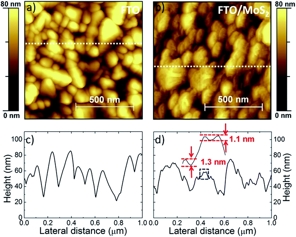 | ||
| Fig. 3 (a) AFM images of FTO and (b) FTO/MoS2. The MoS2 films are deposited from a 0.1 mg mL−1 MoS2 dispersion in IPA. Representative height profiles of (c) FTO and (d) FTO/MoS2 (the corresponding profile positions are shown by the dashed lines in (a) and (b), respectively). In (d), the zoom of the height profile defined by the blue dashed rectangle, showing nano-edge steps, is reported. | ||
MoS2 flakes deposited onto FTO, see Experimental, are subsequently doped by spin coating HAuCl4·3H2O methanol solution on top of the flakes themselves.46,55 The doping process is a consequence of the positive reduction potential of the HAuCl4, which is then prone to accept electrons from MoS2 carrying out the reduction of Au3+ to Au0 species.46,55 As a consequence, the electrical properties of the MoS2 film, i.e., conductivity and WF value, are significantly affected. The doping level is modulated by varying the concentration of HAuCl4·3H2O solutions. Values of concentration of 5, 10, and 20 mM are tested (see details in Experimental, fabrication techniques), giving the MoS2-based films here named as p-MoS2 (5 mM), p-MoS2 (10 mM) and p-MoS2 (20 mM), respectively. Similar dopant concentrations have been already used for engineering the WF of solution-processed MoS2 thin-films for hole transport layers in OPVs.46 The WF value of MoS2, as measured by Kelvin Probe (KP) under ambient conditions (Table 1), is 4.6 eV, thus similar to the one measured for FTO (4.7 eV). After doping, the WF values of the p-MoS2 (5 mM) (4.9 eV) and p-MoS2 (10 mM) (5.1 eV) increase by 0.3 and 0.5 eV, respectively, compared to the one shown by the pristine MoS2 film. Further increase of the doping level up to 20 mM does not reflect an additional rise of the WF value.
| Material | Work function (eV) |
|---|---|
| FTO | 4.7 |
| MoS2 | 4.6 |
| p-MoS2 (5 mM) | 4.9 |
| p-MoS2 (10 mM) | 5.1 |
| p-MoS2 (20 mM) | 5.1 |
Fig. S4† reports the AFM images of the FTO/p-MoS2 (10 mM), which shows no differences in surface morphology with respect to the un-doped case (FTO/MoS2). The roughness average (Ra) values are reported in Table 2, showing a decrease of about 2 nm for both FTO/MoS2 and FTO/p-MoS2 (10 mM) (Ra values of 11.6 nm and 11.9 nm, respectively) if compared with the value of the bare FTO (Ra = 13.8). Thus, the FTO roughness is reduced by the overlayer of MoS2 flakes, which could be linked with their planarity and face-on arrangement.
| Sample | Roughness average (Ra) (nm) |
|---|---|
| FTO | 13.8 |
| FTO/MoS2 | 11.6 |
| FTO/p-MoS2 (10 mM) | 11.9 |
Fig. 4 reports the top view scanning electron microscopy (SEM) images of the FTO, FTO/MoS2, FTO/p-MoS2 (10 mM) and FTO/p-MoS2 (20 mM) samples. No modifications of the FTO surface are observed after the MoS2 flake deposition and doping treatment, i.e., 10 mM HAuCl4·3H2O, in agreement with the AFM data, i.e., Ra values reported in Table 2. The increase of the doping level to 20 mM HAuCl4·3H2O determines the formation of some aggregates, thus affecting the surface's homogeneity, as revealed by Fig. 4d. These aggregates are attributed to the precipitation of Au and MoO3 clusters after Au ion reduction and Mo4+ to Mo6+ conversion processes.46,55 In fact, for the doping level exceeding 10 mM, more electrons are needed to reduce the increased number of Au ions, and thus Mo4+ can be converted into Mo6+, resulting in the formation of Au nanoparticles and MoO3.46,55
 | ||
| Fig. 4 Top view SEM images of the (a) bare FTO, and (b) FTO/MoS2, (c) FTO/p-MoS2 (10 mM) and (d) FTO/p-MoS2 (20 mM) films. The MoS2-based films are deposited from a 0.1 mg mL−1 MoS2 dispersion in IPA. | ||
Architecture of the hybrid solution-processed organic H2-evolving photocathode
The full structure of the solution-processed hybrid organic H2-evolving photocathode consists of a photoactive rr-P3HT:PCBM BHJ sandwiched between solution-processed CSLs. Few-layer MoS2 flakes are spin coated onto FTO and tested as a HSL, while anatase TiO2 nanoparticles are spin coated onto rr-P3HT:PCBM and used as an ESL. Amorphous MoS3 nanoparticles, deposited on top of the TiO2, act as an EC for the HER. Additional details of the fabrication of the photocathodes are reported in Experimental, fabrication techniques.Fig. 5a shows the representative energy band edge positions of the semiconductors of the hybrid photocathode together with the redox levels of the HER and OER. MoS2, as the HSL, is expected to extract the photogenerated holes towards the back conductive substrate (FTO) while the TiO2 (as ESL) transports the photogenerated electrons towards MoS3 (EC). Here, aqueous protons are reduced to H2, which evolves from the photocathode surface.28,29 In order to provide the electrical driving force for the holes' collection,28,29 MoS2 films are doped by spin coating HAuCl4·3H2O methanol solutions on top of them,46,55 thus increasing the WF values of the films from 4.6 eV up to 5.1 eV (for p-MoS2 (10 mM) and p-MoS2 (20 mM), as previously discussed (see also Table 1). Fig. 5b shows the high-resolution cross-sectional SEM image of a representative photocathode FTO/p-MoS2 (10 mM)/rr-P3HT:PCBM/TiO2/MoS3. The layers are consecutively deposited by spin coating (see details in Experimental, fabrication techniques), giving a well-defined multi-layered structure. MoS2 and MoS3 layers are hard to be resolved because their thickness is small with respect to the device-scale magnification. Thicknesses around 150 and 80 nm can be estimated for the rr-P3HT:PCBM and TiO2 layers, respectively. The same thickness values of the rr-P3HT:PCBM layer are also measured by profilometry (see Experimental, fabrication techniques).
 | ||
| Fig. 5 (a) Typical energy band edge position of materials assembled in the hybrid solution-processed photocathode. The rr-P3HT:PCBM layer, in BHJ configuration, efficiently absorbs light and generates charges. MoS2 and TiO2 act as hole- and electron- selective layers (HSL and ESL), respectively, driving the holes towards the FTO substrates and the electrons towards the MoS3 nanoparticles, acting as the EC layer for the HER. Redox levels of both the hydrogen evolution reaction (HER) (blue solid line) and oxygen evolution reaction (OER) (blue dashed line) are also shown. WF values of the MoS2 (4.6 eV) are measured by ambient KP. These values can be tailored to higher values (up to 5.1 eV) by solution-processed treatments using HAuCl4·3H2O as the dopant agent. (b) High-resolution cross-sectional SEM image of the representative photocathode FTO/p-MoS2 (10 mM)/rr-P3HT:PCBM/TiO2/MoS3. | ||
Photoelectrochemical characterization
The rrP3HT:PCBM-based photocathodes using MoS2 and p-MoS2 as HSLs are characterized by linear sweep voltammetry (LSV) in H2SO4 solution at pH 1. The results for MoS2 and p-MoS2 (10 mM) deposited from 0.1 mg mL−1 MoS2 dispersion in IPA are reported in Fig. 6a, where they are compared with the responses of a HSL-free photocathode and the current–potential curve of the MoS3 EC (deposited directly onto FTO). The MoS3 EC reveals activity for the HER, with an onset overpotential of 180 mV with respect to the RHE potential.63 The voltammograms of the photocathodes show a photocurrent that increases when the potential is swept towards negative values. The photocurrents are positively affected by the presence of MoS2 films, thus confirming their role as the HSL. The dependence on the doping level of the p-MoS2-based photocathodes is shown in Fig. 6b. It is worth noting that different concentrations (0.05, 0.1, and 0.4 mg mL−1) of the MoS2 dispersion in IPA have been also preliminary tested without doping (Fig. S5†) and with 10 mM doping (Fig. S6†), showing the best results for the 0.1 mg mL−1 dispersion. | ||
| Fig. 6 (a) LSVs recorded for the photocathodes using MoS2 (orange lines) and p-MoS2 (10 mM) (red lines) as HSLs measured in 0.5 M H2SO4 solution at pH 1, under dark (dashed lines) and AM1.5 light illumination (100 mW cm−2) (solid lines) MoS2 films are deposited by 0.1 mg mL−1 MoS2 dispersion in IPA. The photoelectrochemical responses of the photocathode without any HSL (blue lines) and the current–potential curve of the MoS3 electrocatalyst (deposited directly on FTO) (short dashed black line) are also shown. (b) LSVs recorded for p-MoS2-based photocathodes obtained with different levels of doping (purple, red and magenta lines for 5, 10 and 20 mM HAuCl4·3H2O methanol solution, respectively), under the same previous conditions. | ||
The photovoltage Vphoto is the difference between the potential applied to the photocathode under illumination (Elight) and the potential applied to the catalyst electrode (Edark) to obtain the same current density. The subscript “m” stands for “maximum”. The power-saved FoM (Φsaved,NPAC) reflects the photovoltage and photocurrent of a photocathode independent of the over-potential requirement of the catalyst.64 Here, we simply assume that the MoS3 film deposited onto FTO is identical to the one deposited onto TiO2. Table 3 summarizes the main FoM extracted from the voltammograms recorded for the different cases: the photocurrent density taken at 0 V vs. RHE (J0 V vs. RHE), the Voc, and Φsaved,NPAC, which is calculated by:69

| HSL | J 0 V vs. RHE (mA cm−2) | V oc (V vs. RHE) | Φ saved,NPAC (%) |
|---|---|---|---|
| — | 0.12 | 0.07 | 0.015 |
| MoS2 | 0.30 | 0.30 | 0.070 |
| p-MoS2 (5 mM) | 0.36 | 0.35 | 0.095 |
| p-MoS2 (10 mM) | 1.21 | 0.55 | 0.423 |
| p-MoS2 (20 mM) | 0.54 | 0.49 | 0.192 |
Although the value of the main FoM of the undoped MoS2-based photocathode (J0 V vs. RHE = 0.3 mA cm−2, Voc = 0.3 V vs. RHE, Φsaved,NPAC = 0.070%) increases with respect to the ones of the HSL-free photocathode (J0 V vs. RHE = 0.12 mA cm−2, Voc = 0.07 V vs. RHE, Φsaved,NPAC = 0.015%), significant photocurrents are observed only using p-MoS2 (above 1 mA cm−2 for potential <0.06 V vs. RHE for a doping level of 10 mM). For p-MoS2 (10 mM) and p-MoS2 (20 mM), the presence of a photoreduction peak, located at ∼0.33 V vs. RHE, is also observed. Its origin is attributed to the chemical reduction of the MoS3 EC towards more electrocatalytically active MoS2+x species for the HER,68 as also confirmed by the analysis of two consecutive LSVs of FTO/MoS3 measured under the same testing conditions as the ones reported in Fig. 6 (see ESI Fig. S7†). In the case of p-MoS2 (10 mM), J0 V vs. RHE, Voc and Φsaved,NPAC are 1.21 mA cm−2, 0.56 V vs. RHE and 0.423%, respectively. Photocathodes based on p-MoS2 (20 mM) (highest doping level) and p-MoS2 (5 mM) (lowest doping level) report J0 V vs. RHE of 0.54 and 0.36, thus decreasing by 56% and 70% with respect to the case of p-MoS2 (10 mM), respectively. Concerning p-MoS2 (5 mM), also in this case there is a decrease of the Voc (Voc = 0.35 V vs. RHE) of 200 mV with respect to the values observed for p-MoS2 (10 mM). Moreover, we noted a decrease of 60 mV of the Voc for the p-MoS2 (20 mM) if compared with the p-MoS2 (10 mM) photocathode. The values of Φsaved,NPAC calculated for p-MoS2 (5 mM) and p-MoS2 (20 mM) are 0.095% and 0.192%, respectively. These values correspond to a decrease of 77.5% and 54.6% with respect to that of p-MoS2 (10 mM), respectively.
The obtained results highlight the importance of the WF tuning of the MoS2 films by p-doping treatment for their full-exploitation as highly performant HSLs. Fig. 7 shows the MoS2 doping level dependence of the photocathodes' FoM, as gathered from Table 3. In agreement with the SEM characterization reported in Fig. 4d, the decrease of the J0 V vs. RHE for the p-MoS2 (20 mM) case could be ascribed to charge recombination pathways, i.e., leakage currents, in the presence of blend-uncovered Au and MoO3 clusters. Although these surface alterations of the MoS2 films negatively affect the photocurrents, the Voc value is similar to the one recorded for p-MoS2 (10 mM). Differently, for the case of p-MoS2 (5 mM), we observed a decrease of both the J0 V vs. RHE and the Voc with respect to the p-MoS2 (10 mM) case. This result could be linked with differences (homogeneity) of the MoS2 film doping, as suggested by the lower WF value of p-MoS2 (5 mM) film (4.9 eV) if compared with the ones of p-MoS2 (10 mM) and p-MoS2 (20 mM) films (5.1 eV).
 | ||
| Fig. 7 Dependence of the photocatodes' FoMs (red, blue and black colours for J0 V vs. RHE, Voc and Φsaved,NPAC, respectively) on the HAuCl4·3H2O doping level (from 0 to 20 mM) of the p-MoS2 films. | ||
As a consequence, the main characteristics of the p-MoS2 (5 mM)-based photocathode (Voc ∼ 0.35 V vs. RHE, J0 V vs. RHE ∼ 0.36 mA cm−1 and Φsaved,NPAC ∼ 0.095) are similar to those recorded for the undoped MoS2-based photocathode (Voc ∼ 0.30 V vs. RHE, J0 V vs. RHE ∼ 0.30 mA cm−1 and Φsaved,NPAC ∼ 0.070). To sum up, Voc seems to be linearly correlated with the WF values of the different films, while the J0 V vs. RHE turns out also to be affected by the film surface morphology. The combination of these effects explain the behaviour of the Φsaved,NPAC, whose best value of 0.423% is reached for the p-MoS2 (10 mM)-based photocathode.
The stability test under potentiostatic conditions is performed for p-MoS2 (10 mM) case, recording in time the J0 V vs. RHE under continuous illumination (Fig. 8). The data show an average initial photocurrent value of 1.36 mA cm−2 followed by a steep decrease in performance down to 0.77 mA cm−2 during the first 5 minutes (photocurrent loss of 50.7%). After 30 minutes of continuous operation, the photocurrent density reaches 0.49 mA cm−2 (photocurrent loss of 63.2%). Thus, the photocurrent mainly decreases at the beginning of the illumination process. The quick, initial performance degradation has been recently observed in similar architectures using Pt as the catalyst and CuI as the HSL,29d being attributed to the irreversible Pt detachment from the surface of the electrodes.29d A similar effect could affect the MoS3 EC used here. After more than 5 min, a progressive stabilization is observed. Notably, there is no delamination of the film during the measurements, suggesting the electrochemical stability of the FTO/p-MoS2/P3HT:PCBM under-layers. Moreover, cyclic voltammetry (CV) measurements reveal the absence of irreversible redox reactions involving MoS2 films under the HER-working condition of the photocathodes (see ESI, Fig. S8†). This is in agreement with the electrochemical stability of the MoS2 (ref. 45) expressed in several energy conversion and storage devices,70 including fuel and water splitting cells,71 batteries72 and supercapacitors.73 These results evidence the need for future efforts also in the development of stable ESL/EC layers, for which the integration of TMDs could offer winning solutions thanks to their tuneable charge-selective properties46 and electro-catalytic activity towards the HER.70
 | ||
| Fig. 8 Potentiostatic stability test of the photocathode fabricated with p-MoS2 (10 mM) at pH 1 and 0 V vs. RHE under continuous illumination (1 sun). The blue lines mark the losses of the photocurrent after 5 and 30 min. | ||
Conclusion
Few-layer MoS2 flakes are demonstrated as a novel HSL for solution-processed hybrid organic H2-evolving photocathodes. The production method of the MoS2 flakes underpins on water-based exfoliation of Li-intercalated bulk MoS2, avoiding the use of toxic reagents/solvents and being potentially compatible with large-area and low-cost production. We produced ultrathin MoS2 layers (<10 nm) that, once deposited, do not affect the morphology of the underneath FTO substrate. We tuned the electrical properties of the MoS2 films by using solution-processed HAuCl4·3H2O doping, increasing the WF value from 4.6 up to 5.1 eV, thus well matching with the HOMO level of the rr-P3HT. The morphology of the MoS2 films and the optimization of the HAuCl4·3H2O doping level led to a hybrid solution-processed organic H2-evolving photocathode with J0 V vs. RHE of 1.21 mA cm−2 at 0 V vs. RHE, Voc of 0.56 V vs. RHE and Φsaved,NPAC approaching 0.5%. These results pave the way towards the integration of MoS2 as the HSL in organic PEC cells to boost this technology as an efficient scalable and low-cost tool for solar H2 production.Experimental
Material preparation
MoS2 flakes are prepared by a chemical lithium intercalation method. Experimentally, 0.3 g of MoS2 bulk powder (Sigma Aldrich) is dispersed in 4 mL of 2.0 M n-butyllithium (n-BuLi) in cyclohexane56 (Sigma Aldrich). The dispersion was kept stirring for two days at room temperature under an Ar atmosphere. The Li-intercalated material (LixMoS2) is separated by suction filtration under Ar. LixMoS2 is washed with anhydrous hexane to remove non-intercalated Li ions and organic residues. LixMoS2 powder is then exfoliated by ultrasonication (Branson® 5800 ultrasonic cleaner) in deionized (DI) water for 1 h. The obtained dispersion is then ultracentrifugated (Optima™ XE-90 ultracentrifuge, Beckman Coulter) at 10 K for 20 min to remove LiOH and the un-exfoliated material. Finally, the precipitate is filtered and re-dispersed in IPA (absolute alcohol, without additive, ≥99.8%, Sigma Aldrich), in order to accurately control the concentration of the final dispersions.Fabrication techniques
Photocathodes are fabricated according to the architecture FTO/HSL/rr-P3HT:PCBM/TiO2/MoS3, where few-layer MoS2 flakes are used as the HSL. Complementary architectures without the HSL are also fabricated. FTO coated soda-lime glass substrates (Dyesol, sheet resistance 15 Ω sq−1) are cleaned according to the following protocols: sequential sonication baths in DI water, acetone, and IPA each lasting for 10 minutes and plasma cleaning in an inductively coupled reactor for 20 minutes (100 W RF power, excitation frequency 13.56 MHz, 40 Pa of O2 gas process pressure, background gas pressure 0.2 Pa).The MoS2 dispersion is deposited onto the previously treated FTO by spin coating (Laurell Tech. Corp. Spin coater) using a single step spinning protocol with a rotation speed of 3000 rpm for 60 s. Concentrations of the dispersions of 0.05, 0.1 and 0.4 mg mL−1 are tested. Post-thermal annealing in an Ar atmosphere at 150 °C for 30 min is performed for the MoS2 films. The latter are subsequently doped by spin casting HAuCl4·3H2O (≥99.9% trace metals basis, Sigma Aldrich) in methanol (ACS reagent, ≥99.8%, Sigma Aldrich) solution as p-doping agents on top, by using the same single step spinning protocol of the MoS2 deposition. Doping concentrations of 5, 10, and 20 mM are tested. All doping solutions are sonicated for 10 minutes before deposition. The doped films are subsequently dried for 30 min under an Ar atmosphere. The organic polymer film used in all the architectures consists of a blend of rr-P3HT, as the donor component, and PCBM, as the acceptor component (rr-P3HT:PCBM). rr-P3HT (electronic grade Mn 15![[thin space (1/6-em)]](https://www.rsc.org/images/entities/char_2009.gif) 000–45000, Sigma Aldrich) and PCBM (99.5% purity, Nano C) are separately dissolved in chlorobenzene (ACS grade, Sigma Aldrich), at a 1:1 wt ratio and 25 mg mL−1 on a polymer basis. Polymer blend solution is stirred at 40 °C for 24 hours before use. Blend thin films are obtained by spin casting the rr-P3HT:PCBM solution using the following set of parameters: two step spinning protocol with rotation speeds of 800 rpm for 3 s followed by 1600 rpm for 60 s, respectively. This spin casting protocol produced a rr-P3HT:PCBM blend layer 200 ± 20 nm thick, as measured by means of a Dektak XT profilometer (Bruker) equipped with a diamond-tipped stylus (2 mm) selecting a vertical scan range of 25 mm with 8 nm resolution and a stylus force of 1 mN, on an area of 0.25 cm2. The sol–gel procedure for producing the TiO2 dispersion has been previously reported by Kim et al.74 Thus, TiO2 precursor solution is prepared in IPA and subsequently deposited by spin casting on top of the rr-P3HT:PCBM film as the ESL. Subsequently, during 12 h in air at room temperature, the precursor converted to TiO2 by hydrolysis. A three step spinning protocol with rotation speeds of 200 rpm for 3 s, 1000 rpm for 60 s and 5000 rpm for 30 s is used. Post-thermal annealing in an Ar atmosphere is carried out at 130 °C for 10 min for all the devices before catalyst deposition. The devices are completed by a layer of MoS3 nanoparticles (Alfa Aesar) acting as the catalyst for the HER process. The catalyst layer is obtained by spin casting a 3.8 mg mL−1 water:acetone:NaOH (1 M) 1:2:0.2 dispersion on top of the TiO2. The dispersion is stirred overnight at room temperature and sonicated for 10 minutes before its use. The spinning protocol is identical to the one adopted for the TiO2 deposition.
000–45000, Sigma Aldrich) and PCBM (99.5% purity, Nano C) are separately dissolved in chlorobenzene (ACS grade, Sigma Aldrich), at a 1:1 wt ratio and 25 mg mL−1 on a polymer basis. Polymer blend solution is stirred at 40 °C for 24 hours before use. Blend thin films are obtained by spin casting the rr-P3HT:PCBM solution using the following set of parameters: two step spinning protocol with rotation speeds of 800 rpm for 3 s followed by 1600 rpm for 60 s, respectively. This spin casting protocol produced a rr-P3HT:PCBM blend layer 200 ± 20 nm thick, as measured by means of a Dektak XT profilometer (Bruker) equipped with a diamond-tipped stylus (2 mm) selecting a vertical scan range of 25 mm with 8 nm resolution and a stylus force of 1 mN, on an area of 0.25 cm2. The sol–gel procedure for producing the TiO2 dispersion has been previously reported by Kim et al.74 Thus, TiO2 precursor solution is prepared in IPA and subsequently deposited by spin casting on top of the rr-P3HT:PCBM film as the ESL. Subsequently, during 12 h in air at room temperature, the precursor converted to TiO2 by hydrolysis. A three step spinning protocol with rotation speeds of 200 rpm for 3 s, 1000 rpm for 60 s and 5000 rpm for 30 s is used. Post-thermal annealing in an Ar atmosphere is carried out at 130 °C for 10 min for all the devices before catalyst deposition. The devices are completed by a layer of MoS3 nanoparticles (Alfa Aesar) acting as the catalyst for the HER process. The catalyst layer is obtained by spin casting a 3.8 mg mL−1 water:acetone:NaOH (1 M) 1:2:0.2 dispersion on top of the TiO2. The dispersion is stirred overnight at room temperature and sonicated for 10 minutes before its use. The spinning protocol is identical to the one adopted for the TiO2 deposition.
Material characterization
The UV-Vis absorption spectrum of the 0.1 mg mL−1 MoS2 dispersion in IPA is obtained using a Cary Varian 5000UV-Vis spectrometer.Raman measurements are carried out with a Renishaw 1000 using a 50× objective, a laser with a wavelength of 532 nm and an incident power of 1 mW. The different peaks are fitted with Lorentzian functions. For each sample 30 spectra are collected. 0.01 mg mL−1 MoS2 dispersion in IPA is drop-cast onto the Si/SiO2 (300 nm SiO2) substrate and dried under vacuum. Statistical analysis of the relevant features is carried out by means of software Origin 8.1 (OriginLab).
The XPS analysis is carried out using a Kratos Axis Ultra spectrometer on MoS2 flakes drop cast onto 50 nm-Au sputtered coated Si wafers from the 0.1 mg mL−1 dispersion in IPA. The XPS spectra are acquired using a monochromatic Al Kα source operated at 20 mA and 15 kV. High-resolution spectra are collected with a pass energy of 10 eV and energy step of 0.1 eV over a 300 μm × 700 μm area. The Kratos charge neutralizer system is used on all specimens. Spectra are charge corrected to the main line of the C1s spectrum set to 284.8 eV, and analyzed with CasaXPS software (version 2.3.17).
Transmission electron microscopy images are taken on a JEM 1011 (JEOL) transmission electron microscope, operating at 100 kV. 0.01 mg mL−1 MoS2 dispersions in IPA are drop-cast onto carbon coated Cu TEM grids (300 mesh), rinsed with DI water and subsequently dried under vacuum overnight. The lateral dimension of the MoS2 flakes is measured using ImageJ software (Java). Statistical TEM analysis is carried out by means of software Origin 8.1 (OriginLab).
Scanning electron microscopy analysis is carried out with a FEI Helios Nano lab field-emission scanning electron microscope. The samples are imaged without any metal coating or pre-treatment. The samples are prepared depositing MoS2 films on FTO as described in the Fabrication techniques section.
Atomic force microscopy images are obtained using a commercial AFM instrument MFP-3D (Asylum Research), with NSG30/Au (NT-MDT) probes in tapping mode in air. These golden silicon probes have a nominal resonance frequency and spring constant of 240–440 kHz and 22–100 N m−1, respectively. The tip is a pyramid with 14–16 μm length and ∼20 nm apex diameter. The images are processed with the AFM company software Version-13, based on IgorPro 6.22 (Wavemetrics). MoS2 is deposited onto FTO as described in the previous section (Fabrication techniques). Images of MoS2 flakes deposited onto mica sheets (EMS) (V-1 quality) are also acquired in order to extrapolate the average thickness of single flakes. MoS2 flakes are deposited by drop casting from 0.1 mg mL−1 MoS2 dispersion in IPA. Statistical analysis of the height profiles is carried out by means of software Origin 8.1 (OriginLab).
Work function data are obtained by using a commercial kelvin probe system (KPSP020, KP Technologies Inc.). Samples are measured in air and at room temperature and both a clean gold surface (WF = 4.8 eV) and a graphite sample (HOPG, highly ordered pyrolytic graphite, WF = 4.6 eV) are used as independent references for the probe potential.
Photoelectrochemical measurements
Photoelectrochemical measurements are carried out at room temperature in a flat-bottom fused silica cell under a three-electrode configuration using a CompactStat potentiostat/galvanostat station (Ivium), controlled via Ivium's own IviumSoft. A Pt wire is used as the counter-electrode and sat. KCl Ag/AgCl is used as the reference electrode. Measurements are performed in 50 mL aqueous solution of 0.5 M H2SO4 (99.999% purity, Sigma Aldrich) at pH 1. Oxygen is purged from electrolyte solutions by flowing nitrogen gas throughout the liquid volume using a porous frit at least 30 minutes before starting measurements. A constant, slight nitrogen flow is maintained afterwards for the whole duration of experiments, to avoid re-dissolution of molecular oxygen in the electrolyte. Potential differences between the working electrode and the reference electrode are reported with respect to the RHE scale using the Nernst equation. A 300 W Xenon light source LS0306 (Lot Quantum Design), equipped with AM1.5G filters, is used to simulate solar illumination (1 sun) at the glass substrate side of the samples inside the test cell. Linear Sweep Voltammetry is used to evaluate the response of devices in the dark and under 1 sun illumination. Voltage is swept starting from the Voc of the photocathodes to a negative potential of −0.3 V vs. RHE at a scan rate of 10 mV s−1. The stability test is performed by recording in time the J0 V vs. RHE under continuous illumination (1 sun) at 0 V vs. RHE. Cyclic voltammetry (CV) is carried out on MoS2 films deposited on glassy carbon substrates (Sigma Aldrich) (previously cleaned with IPA) by consequent drop casting steps from 0.4 mg mL−1 MoS2 dispersion in IPA (until reaching a loading of MoS2 of 0.5 mg cm−1). The voltage scan rate is 200 mV s−1.Acknowledgements
We acknowledge M. Prato for useful discussion. This project has received funding from the European Union's Horizon 2020 research and innovation program under grant agreement No. 696656—GrapheneCore1, and from the FP7 FET Collaborative Project PHOCS, under grant agreement n. 309223.Notes and references
- I. Dincer, Renewable Sustainable Energy Rev., 2000, 4(2), 157–175 CrossRef.
- Y. Tachibana, L. Vayssieres and J. R. Durrant, Nat. Photonics, 2012, 6, 511 CrossRef CAS.
- (a) M. G. Walter, E. L. Warren, J. R. McKone, S. W. Boettcher, Q. Mi, E. A. Santori and N. S. Lewis, Chem. Rev., 2010, 110, 6446–6473 CrossRef CAS PubMed; (b) K. Sivula, F. L. Formal and M. Grätzel, ChemSusChem, 2011, 4, 432–449 CrossRef CAS PubMed.
- D. Wei and G. Amaratunga, Int. J. Electrochem. Sci., 2007, 2, 897–912 Search PubMed.
- R. van de Krol and M. Grätzel, Photoelectrochemical Hydrogen Production, Springer, 2012 Search PubMed.
- H. Zhang, Q. Ding, D. He, H. Liu, W. Liu, Z. Li, B. Yang, X. Zhang, L. Lei and S. Jin, Energy Environ. Sci., 2016, 9(10), 3113–3119 CAS.
- (a) L. Gao, Y. Cui, R. H. J. Vervuurt, D. van Dam, R. P. J. van Veldhoven, J. P. Hofmann, A. A. Bol, J. E. M. Haverkort, P. H. L. Notten, E. P. A. M. Bakkers and E. J. M. Hensen, Adv. Funct. Mater., 2016, 26, 679–686 CrossRef CAS; (b) J. L. Young, K. X. Steirer, M. J. Dzara, J. A. Turner and T. G. Deutsch, J. Mater. Chem. A, 2016, 4, 2831–2836 RSC.
- (a) Z. Chen, T. F. Jaramillo, T. G. Deutsch, A. Kleiman-Shwarsctein, A. J. Forman, N. Gaillard, R. Garland, K. Takanabe, C. Heske and M. Sunkara, et al. , J. Mater. Res., 2010, 25, 3–16 CrossRef CAS; (b) H. Döscher, J. L. Young, J. F. Geisz, J. A. Turner and T. G. Deutsch, Energy Environ. Sci., 2016, 9, 74–80 RSC; (c) Z. Li, W. Luo, M. Zhang, J. Feng and Z. Zoua, Energy Environ. Sci., 2013, 6, 347–370 RSC; (d) S. Hu, C. Xiang, S. Haussener, A. D. Berger and N. S. Lewis, Energy Environ. Sci., 2013, 6, 2984 RSC.
- M. S. Prévot and K. Sivula, J. Phys. Chem. C, 2013, 117, 17879–17893 Search PubMed.
- (a) K.-S. Ahn, Y. Yan, S.-H. Lee, T. Deutsch, J. Turner, C. E. Tracy, C. L. Perkins and M. Al-Jassim, J. Electrochem. Soc., 2007, 154, B956–B959 CrossRef CAS; (b) X. Yang, A. Wolcott, G. Wang, A. Sobo, R. C. Fitzmorris, F. Qian, J. Z. Zhang and Y. Li, Nano Lett., 2009, 9, 2331–2336 CrossRef CAS PubMed.
- (a) Y. J. Lin, G. B. Yuan, S. Sheehan, S. Zhou and D. W. Wang, Energy Environ. Sci., 2011, 4, 4862–4869 RSC; (b) D. K. Zhong, M. Cornuz, K. Sivula, M. Grätzel and D. R. Gamelin, Energy Environ. Sci., 2011, 4, 1759–1764 RSC; (c) B. D. Alexander, P. J. Kulesza, I. Rutkowska, R. Solarska and J. Augustynski, J. Mater. Chem., 2008, 18, 2298–2303 RSC.
- (a) A. J. Bard and M. A. Fox, Acc. Chem. Res., 1995, 28, 141–145 CrossRef CAS; (b) A. B. Murphy, P. R. F. Barnes, L. K. Randeniya, I. C. Plumb, I. E. Grey, M. D. Horne and J. A. Glasscock, Int. J. Hydrogen Energy, 2006, 31, 1999–2017 CrossRef CAS.
- W. J. Luo, Z. S. Yang, Z. S. Li, J. Y. Zhang, J. G. Liu, Z. Y. Zhao, Z. Q. Wang, S. C. Yan, T. Yu and Z. G. Zou, Energy Environ. Sci., 2011, 4, 4046–4051 CAS.
- T. M. Suzuki, S. Saeki, K. Sekizawa, K. Kitazumi, N. Takahashi and T. Morikawa, Appl. Catal., B, 2017, 202, 597–604 CrossRef CAS.
- (a) R. Abe, M. Higashi and K. Domen, J. Am. Chem. Soc., 2010, 132, 11828–11829 CrossRef CAS PubMed; (b) M. Higashi, R. Abe and K. Domen, Energy Environ. Sci., 2011, 4, 4138–4147 RSC; (c) M. J. Liao, J. Y. Feng, W. J. Luo, Z. Q. Wang, J. Y. Zhang, Z. S. Li, T. Yu and Z. G. Zou, Adv. Funct. Mater., 2012, 22, 3066–3074 CrossRef CAS; (d) D. Lu, G. Hitoki, E. Katou, J. N. Kondo, M. Hara and K. Domen, Chem. Mater., 2004, 16(9), 1603–1605 CrossRef CAS; (e) Z. Wang, Y. Qi, C. Ding, D. Fan, G. Liu, Y. Zhao and C. Li, Chem. Sci., 2016, 7, 4391–4399 RSC; (f) Z. Wang, Y. Qi, C. Ding, A. D. Fan, G. Liu, Y. Zhao and C. Li, Chem. Sci., 2016, 7, 4391 RSC.
- O. Khaselev and J. A. Turner, Science, 1998, 280, 425–427 CrossRef CAS PubMed.
- (a) S. Licht, B. Wang, S. Mukerji, T. Soga, M. Umeno and H. Tributsch, Int. J. Hydrogen Energy, 2001, 26, 653–659 CrossRef CAS; (b) G. Peharz, F. Dimroth and U. Wittstadt, Int. J. Hydrogen Energy, 2007, 32, 3248–3252 CrossRef CAS.
- (a) A. Paracchino, V. Laporte, K. Sivula, M. Grätzel and E. Thimsen, Nat. Mater., 2011, 10(6), 456–461 CrossRef CAS PubMed; (b) A. Paracchino, N. Mathews, T. Hisatomi, M. Stefik, S. D. Tilley and M. Grätzel, Energy Environ. Sci., 2012, 5, 8673–8681 RSC; (c) A. A. Dubale, A. G. Tamirat, H.-M. Chen, T. A. Berhe, C.-J. Pan, W.-N. Su and B.-J. Hwang, J. Mater. Chem. A, 2016, 4, 2205–2216 RSC.
- (a) F. Chen, Q. Zhu, Y. Wang, W. Cui, X. Su and Y. Li, ACS Appl. Mater. Interfaces, 2016, 8, 31025–31031 CrossRef CAS PubMed; (b) B. Fabre, G. Li, F. Gouttefangeas, L. Joanny and G. Loget, Langmuir, 2016, 32, 11728–11735 CrossRef CAS PubMed; (c) K. C. Kwon, S. Choi, K. Hon, C. W. Moon, Y.-S. Shim, D. H. Kim, T. Kim, W. Sohn, J.-M. Jeon, C.-H. Le, K. T. Na, S. Ha, S. Y. Kim and H. W. Jang, Energy Environ. Sci., 2016, 9, 2240–2248 RSC.
- J. Luo, Z. Li, S. Nishiwaki, M. Schreier, M. T. Mayer, P. Cendula, Y. H. Lee, K. Fu, A. Cao, M. K. Nazeeruddin, Y. E. Romanyuk, S. Buecheler, S. D. Tilley, L. H. Wong, A. N. Tiwari and M. Grätzel, Adv. Energy Mater., 2015, 5, 1501520 CrossRef.
- Gurudayal, D. Sabba, M. H. Kumar, L. H. Wong, J. Barber, M. Grätzel and N. Mathews, Nano Lett., 2015, 15(6), 3833–3839 CrossRef CAS PubMed.
- S. Hu, N. S. Lewis, J. W. Ager, J. Yang, J. R. McKone and N. C. Strandwitz, J. Phys. Chem. C, 2015, 119(43), 24201–24228 CAS.
- M. Crespo-Quesada, L. M. Pazos-Outón, J. Warnan, M. F. Kuehnel, R. H. Friend and E. Reisner, Nat. Commun., 2016, 7, 12555, DOI:10.1038/ncomms12555.
- (a) X. Wang, K. Maeda, A. Thomas, K. Takanabe, G. Xin, J. M. Carlsson, K. Domen and M. Antonietti, Nat. Mater., 2009, 8, 76 CrossRef CAS PubMed; (b) G. Zhang and X. Wang, J. Catal., 2013, 307, 246 CrossRef CAS; (c) S. Martha, A. Nashim and K. M. Parida, J. Mater. Chem. A, 2013, 1, 7816 RSC; (d) X. Wang, K. Maeda, X. Chen, K. Takanabe, K. Domen, Y. Hou, X. Fu and M. Antonietti, J. Am. Chem. Soc., 2009, 131, 1680 CrossRef CAS PubMed; (e) K. Kailasam, J. D. Epping, A. Thomas, S. Losse and H. Junge, Energy Environ. Sci., 2011, 4, 4668 RSC.
- (a) L. Stegbauer, K. Schwinghammer and B. V. Lotsch, Chem. Sci., 2014, 5, 2789 RSC; (b) J. H. Park, K. C. Ko, N. Park, H.-W. Shin, E. Kim, N. Kang, J. H. Ko, S. M. Lee, H. J. Kim, T. K. Ahn, J. Y. Lee and S. U. Son, J. Mater. Chem. A, 2014, 2, 7656 RSC.
- (a) M. Jakešová, D. H. Apaydin, M. Sytnyk, K. Oppelt, W. Heiss, N. S. Sariciftci and E. D. Głowacki, Adv. Funct. Mater., 2016, 26, 5248–5254 CrossRef; (b) A. Morozan, T. Bourgeteau, D. Tondelier, B. Geffroy, B. Jousselme and V. Artero, Nanotechnology, 2016, 27(35), 355401 CrossRef CAS PubMed.
- R. S. Sprick, J.-X. Jiang, B. Bonillo, S. Ren, T. Ratvijitvech, P. Guiglion, M. A. Zwijnenburg, D. J. Adams and A. I. Cooper, J. Am. Chem. Soc., 2015, 137, 3265 CrossRef CAS PubMed.
- (a) M. Haro, C. Solis, G. Molina, L. Otero, J. Bisquert, S. Gimenez and A. Guerrero, J. Phys. Chem. C, 2015, 119, 6488 CrossRef CAS; (b) M. P. Gustafson, N. Clark, B. Winther-Jensen and D. R. MacFarlane, Electrochim. Acta, 2014, 140, 309 CrossRef CAS; (c) L.-H. Lai, W. Gomulya, M. Berghuis, L. Protesescu, R. J. Detz, J. N. H. Reek, M. V. Kovalenko and M. A. Loi, ACS Appl. Mater. Interfaces, 2015, 7, 19083 CrossRef CAS PubMed; (d) T. Bourgeteau, D. Tondelier, B. Geffroy, R. Brisse, C. Laberty-Robert, S. Campidelli, R. de Bettignies, V. Artero, S. Palacin and B. Jousselme, Energy Environ. Sci., 2013, 6, 2706 RSC; (e) M. Haro, C. Solis, V. M. Blas-Ferrando, O. Margeat, S. B. Dhkil, C. Videlot-Ackermann, J. Ackermann, F. Di Fonzo, A. Guerrero and S. Gimenez, ChemSusChem, 2016, 9, 3062–3066 CrossRef CAS PubMed.
- (a) T. Bourgeteau, D. Tondelier, B. Geffroy, R. Brisse, S. Campidelli, R. Cornut and B. Jousselme, J. Mater. Chem. A, 2016, 4, 4831–4839 RSC; (b) F. Fumagalli, S. Bellani, M. Schreier, S. Leonardi, H. C. Rojas, A. Ghadirzadeh, G. Tullii, A. Savoini, G. Marra, L. Meda, M. Grätzel, G. Lanzani, M. T. Mayer, M. R. Antognazza and F. Di Fonzo, J. Mater. Chem. A, 2016, 4, 2178–2187 RSC; (c) T. Bourgeteau, D. Tondelier, B. Geffroy, R. Brisse, R. Cornut, V. Artero and B. Jousselme, ACS Appl. Mater. Interfaces, 2015, 7, 16395 CrossRef CAS PubMed; (d) H. C. Rojas, S. Bellani, F. Fumagalli, G. Tullii, S. Leonardi, M. T. Mayer, M. R. Schreier, M. Grätzel, G. Lanzani, F. D. Fonzo and M. R. Antognazza, Energy Environ. Sci., 2016, 9, 3710–3723 RSC; (e) A. Mezzetti, F. Fumagalli, A. Alfano, D. Iadicicco, M. R. Antognazza and F. Di Fonzo, Faraday Discuss., 2016 10.1039/c6fd00216a.
- (a) A. Marrocchi, D. Lanari, A. Facchetti and L. Vaccaro, Energy Environ. Sci., 2012, 5, 8457 RSC; (b) G. Li, R. Zhui and Y. Yang, Nat. Photonics, 2012, 6, 153–161 CrossRef CAS; (c) A. Capasso, L. Salamandra, A. Di Carlo, J. M. Bell and N. Motta, Beilstein J. Nanotechnol., 2011, 3(1), 524–532 Search PubMed.
- H. J. Park, J. Y. Lee, T. Lee and L. J. Guo, Adv. Energy Mater., 2013, 3, 1135 CrossRef CAS.
- (a) G. Suppes, E. Ballard and S. Holdcroft, Polym. Chem., 2013, 4, 5345 RSC; (b) E. Lanzarini, M. R. Antognazza, M. Biso, A. Ansaldo, L. Laudato, P. Bruno, P. Metrangolo, G. Resnati, D. Ricci and G. Lanzani, J. Phys. Chem. C, 2012, 116, 10944 CrossRef CAS; (c) S. Bellani, A. Ghadirzadeh, L. Meda, A. Savoini, A. Tacca, G. Marra, R. Meira, J. Morgado, F. Di Fonzo and M. R. Antognazza, Adv. Funct. Mater., 2015, 25, 4531 CrossRef CAS.
- (a) S. Bellani, D. Fazzi, P. Bruno, E. Giussani, E. V. Canesi, G. Lanzani and M. R. Antognazza, J. Phys. Chem. C, 2014, 118, 6291 CrossRef CAS; (b) M. R. Antognazza, D. Ghezzi, D. Musitelli, M. Garbugli and G. Lanzani, Appl. Phys. Lett., 2009, 94, 243501 CrossRef; (c) S. Vaquero, C. Bossio, S. Bellani, N. Martino, E. Zucchetti, G. Lanzani and M. R. Antognazza, J. Mater. Chem. B, 2016, 4, 5272–5283 RSC; (d) S. Bellani, M. Porro, C. Caddeo, M. I. Saba, P. B. Miranda, A. Mattoni, G. Lanzani and M. R. Antognazza, J. Mater. Chem. B, 2015, 3, 6429–6438 RSC; (e) E. Mosconi, P. Salvatori, M. I. Saba, A. Mattoni, S. Bellani, F. Bruni, B. Santiago Gonzalez, M. R. Antognazza, S. Brovelli, G. Lanzani, H. Li, J.-L. Brédas and F. De Angelis, ACS Energy Lett., 2016, 1, 454–463 CrossRef CAS; (f) R. Porrazzo, S. Bellani, A. Luzio, C. Bertarelli, G. Lanzani, M. Caironi and M. R. Antognazza, APL Mater., 2015, 3(1), 014905 CrossRef; (g) R. M. Girón, J. Marco-Martínez, S. Bellani, A. Insuasty, H. C. Rojas, G. Tullii, M. R. Antognazza, S. Filippone and N. Martín, J. Mater. Chem. A, 2016, 4, 14284–14290 RSC.
- A. Guerrero, M. Haro, S. Bellani, M. R. Antognazza, L. Meda, S. Gimenez and J. Bisquert, Energy Environ. Sci., 2014, 7, 3666 CAS.
- (a) R. Steim, F. R. Koglera and C. J. Brabec, J. Mater. Chem., 2010, 20, 2499–2512 RSC; (b) A. Capasso, L. Salamandra, A. Chou, A. Di Carlo and N. Motta, Sol. Energy Mater. Sol. Cells, 2013, 122, 297–302 CrossRef.
- K. Sun, S. Zhang, P. Li, Y. Xia, X. Zhang, D. Du, F. H. Isikgor and J. Ouyang, J. Mater. Sci.: Mater. Electron., 2015, 26(7), 4438–4462 CrossRef CAS.
- Z. He, B. Xiao, F. Liu, H. Wu, Y. Yang, S. Xiao, C. Wang, T. P. Russell and Y. Cao, Nat. Photonics, 2015, 9, 174 CrossRef CAS.
- E. Stavrinidou, P. Leleux, H. Rajaona, D. Khodagholy, J. Rivnay, M. Lindau, S. Sanaur and G. G. Malliaras, Adv. Mater., 2013, 25, 4488 CrossRef CAS PubMed.
- Q. Huang, Z. Ye and X. Xiao, J. Mater. Chem. A, 2015, 3, 15824–15837 CAS.
- N. Balis, E. Stratakis and E. Kymakis, Mater. Today, 2016, 19, 580–594 CrossRef CAS.
- M.-L. Tsai, S.-H. Su, J.-K. Chang, D.-S. Tsai, C.-H. Chen, C.-I. Wu, L.-J. Li, L.-J. Chen and J.-H. He, ACS Nano, 2014, 8(8), 8317–8322 CrossRef CAS PubMed.
- W. Liu, X. Yang, Y. Zhang, M. Xu and H. Chen, RSC Adv., 2014, 4, 32744 RSC.
- (a) F. Bonaccorso, L. Colombo, G. Yu, M. Stoller, V. Tozzini, A. C. Ferrari, R. S. Ruoff and V. Pellegrini, Science, 2015, 347, 1246501 CrossRef PubMed; (b) A. C. Ferrari, et al. , Nanoscale, 2015, 7, 4598–4810 RSC; (c) K. F. Mak and J. Shan, Nat. Photonics, 2016, 10, 216–226 CrossRef CAS; (d) X. Duan, C. Wang, A. Pan, R. Yu and X. Duan, Chem. Soc. Rev., 2015, 44, 8859 RSC; (e) A. A. Tedstone, D. J. Lewis and P. O'Brien, Chem. Mater., 2016, 28, 1965–1974 CrossRef CAS.
- (a) W. Choi, M. Y. Cho, A. Konar, J. H. Lee, G.-B. Cha, S. C. Hong, S. Kim, J. Kim, D. Jena, J. Joo and S. Kim, Adv. Mater., 2012, 24, 5832–5836 CrossRef CAS PubMed; (b) M. Bernardi, M. Palummo and J. C. Grossman, Nano Lett., 2013, 13(8), 3664–3670 CrossRef CAS PubMed.
- (a) S. Kim, A. Konar, W.-S. Hwang, J. H. Lee, J. Lee, J. Yang, C. Jung, H. Kim, J.-B. Yoo, J.-Y. Choi, Y. W. Jin, S. Y. Lee, D. Jena, W. Choi and K. Kim, Nat. Commun., 2012, 3, 1011 CrossRef PubMed; (b) Bao, X. Cai, D. Kim, K. Sridhara and M. S. Fuhrer, Appl. Phys. Lett., 2013, 102, 042104 CrossRef; (c) H. Zhang, ACS Nano, 2015, 9(10), 9451–9469 CrossRef CAS PubMed.
- J.-M. Yun, Y.-J. Noh, J.-S. Yeo, Y.-J. Go, S.-I. Na, H.-G. Jeong, J. Kim, S. Lee, S.-S. Kim, H. Y. Koo, T.-W. Kim and D.-Y. Kim, J. Mater. Chem. C, 2013, 1, 3777–3783 RSC.
- X. Gu, W. Cui, H. Li, Z. Wu, Z. Zeng, S.-T. Lee, H. Zhang and B. Sun, Adv. Energy Mater., 2013, 3, 1262 CrossRef CAS.
- X. Fan, C. Cui, G. Fang, J. Wang, S. Li, F. Cheng, H. Long and Y. Li, Adv. Funct. Mater., 2012, 22, 585 CrossRef CAS.
- Y. Kim, A. M. Ballantyne, J. Nelson and D. D. C. Bradley, Org. Electron., 2009, 10, 205–209 CrossRef CAS.
- Y. G. Kim, K. C. Kwon, Q. V. Le, K. Hong, H. W. Jang and S. Y. Kim, J. Power Sources, 2016, 319, 1–8 CrossRef CAS.
- A. Capasso, F. Matteocci, L. Najafi, M. Prato, J. Buha, L. Cinà, V. Pellegrini, A. Di Carlo and F. Bonaccorso, Adv. Energy Mater., 2016, 6(16), 1600920 CrossRef.
- (a) W. Nie, H. Tsai, R. Asadpour, J. C. Blancon, A. J. Neukirch, G. Gupta, J. J. Crochet, M. Chhowalla, S. Tretiak, M. A. Alam, H. L. Wang and A. D. Mohite, Science, 2015, 247, 522 CrossRef PubMed; (b) J. Seo, S. Park, Y. C. Kim, N. J. Jeon, J. H. Noh, S. C. Yoon and S. I. Seok, Energy Environ. Sci., 2014, 7, 2642 RSC; (c) C. W. Chen, H. W. Kang, S. Y. Hsiao, P. F. Yang, K. M. Chiang and H. W. Lin, Adv. Mater., 2014, 26, 6647 CrossRef CAS PubMed.
- (a) H. Zhou, Q. Chen, G. Li, S. Luo, T.-b. Song, H.-S. Duan, Z. Hong, J. You, Y. Liu and Y. Yang, Science, 2014, 345, 542–546 CrossRef CAS PubMed; (b) J.-H. Im, I.-H. Jang, N. Pellet, M. Grätzel and N.-G. Park, Nat. Nanotechnol., 2014, 2, 705 Search PubMed; (c) W. Nie, H. Tsai, R. Asadpour, J.-C. Blancon, A. J. Neukirch, G. Gupta, J. J. Crochet, M. Chhowalla, S. Tretiak, M. A. Alam, H.-L. Wang and A. D. Mohite, Science, 2015, 347, 522–525 CrossRef CAS PubMed; (d) M. A. Green, A. Ho-Baillie and H. J. Snaith, Nat. Photonics, 2014, 8, 506–514 CrossRef CAS.
- (a) V. Nicolosi, M. Chhowalla, M. G. Kanatzidis, M. S. Strano and J. N. Coleman, Science, 2013, 340, 1226419 CrossRef; (b) Z. Zeng, Z. Yin, X. Huang, H. Li, Q. He, G. Lu, F. Boey and H. Zhang, Angew. Chem., Int. Ed., 2011, 50, 11093 CrossRef CAS PubMed; (c) F. Bonaccorso, A. Bartolotta, J. N. Coleman and C. Backes, Adv. Mater., 2016, 28, 6136–6166 CrossRef CAS PubMed; (d) L. Niu, J. N. Coleman, H. Zhang, H. Shin, M. Chhowalla and Z. Zheng, Small, 2016, 12(3), 272–293 CrossRef CAS PubMed.
- (a) Y. Shi, K. K. Kim, A. Reina, M. Hofmann, L. J. Li and J. Kong, ACS Nano, 2010, 4, 2689 CrossRef CAS PubMed; (b) K. C. Kwon, K. S. Choi and S. Y. Kim, Adv. Funct. Mater., 2012, 22, 4724 CrossRef CAS.
- H. S. Matte, A. Gomathi, A. K. Manna, D. J. Late, R. Datta, S. K. Pati and C. N. Rao, Angew. Chem., Int. Ed. Engl., 2010, 49(24), 4059–4062 CrossRef CAS PubMed.
- (a) H. Li, Z. Yin, Q. He, H. Li, X. Huang, G. Lu, D. W. H. Fam, A. I. Y. Tok, Q. Zhang and H. Zhang, Small, 2012, 8, 63–67 CrossRef CAS PubMed; (b) Y.-H. Lee, X.-Q. Zhang, W. Zhang, M.-T. Chang, C.-T. Lin, K.-D. Chang, Y.-C. Yu, J. T.-W. Wang, C.-S. Chang, L.-J. Li and T.-W. Lin, Adv. Mater., 2012, 24, 2320–2325 CrossRef CAS PubMed; (c) M. M. Benameur, B. Radisavljevic, S. Sahoo, H. Berger and A. Kis, Nanotechnology, 2011, 22(12), 125706 CrossRef CAS PubMed; (d) B. Radisavljevic, A. Radenovic, J. Brivio, V. Giacometti and A. Kis, Nat. Nanotechnol., 2011, 6, 147–150 CrossRef CAS PubMed.
- A. Jawaid, D. Nepal, K. Park, M. Jespersen, A. Qualley, P. Mirau, L. F. Drummy and R. A. Vaia, Chem. Mater., 2016, 28, 337 CrossRef CAS.
- U. Halim, C. R. Zheng, Y. Chen, Z. Lin, S. Jiang, R. Cheng, Y. Huang and X. Duan, Nat. Commun., 2013, 4, 2213 Search PubMed.
- P. Joensen, R. F. Frindt and S. R. Morrison, Mater. Res. Bull., 1986, 21(4), 457–461 CrossRef CAS.
- (a) F. Dybała, M. P. Polak, J. Kopaczek, P. Scharoch, K. Wu, S. Tongay and R. Kudrawiec, Sci. Rep., 2016, 6, 26663 CrossRef PubMed; (b) K. F. Mak, C. Lee, J. Hone, J. Shan and T. F. Heinz, Phys. Rev. Lett., 2010, 105, 136805 CrossRef PubMed; (c) W. Zhao, R. M. Ribeiro, M. Toh, A. Carvalho, C. Kloc, A. H. C. Neto and G. Eda, Nano Lett., 2013, 13(11), 5627–5634 CrossRef CAS PubMed; (d) J. Kopaczek, M. P. Polak, P. Scharoch, K. Wu, B. Chen, S. Tongay and R. Kudrawiec, J. Appl. Phys., 2016, 119, 235705 CrossRef; (e) S. J. Sandoval, D. Yang, R. F. Frindt and J. C. Irwin, Phys. Rev. B: Condens. Matter Mater. Phys., 1991, 44, 3955 CrossRef.
- G. Eda, H. Yamaguchi, D. Voiry, T. Fujita, M. Chen and M. Chhowalla, Nano Lett., 2011, 11(12), 5111–5116 CrossRef CAS PubMed.
- H. Zhang, S. B. Lu, J. Zheng, J. Du, S. C. Wen, D. Y. Tang and K. P. Loh, Opt. Express, 2014, 22(6), 7249–7260 CrossRef CAS PubMed.
- (a) A. Molina-Sanchez and L. Wirtz, Phys. Rev. B: Condens. Matter Mater. Phys., 2011, 84(15), 155413 CrossRef; (b) R. Saito, Y. Tatsumi, S. Huang, X. Ling and M. S. Dresselhaus, J. Phys.: Condens. Matter, 2016, 28(35), 353002 CrossRef CAS PubMed.
- (a) H. Li, Q. Zhang, C. C. R. Yap, B. K. Tay, T. H. T. Edwin, A. Olivier and D. Baillargeat, Adv. Funct. Mater., 2012, 22, 1385–1390 CrossRef CAS; (b) A. C. Ferrari and D. M. Basko, Nat. Nanotechnol., 2013, 8, 235–246 CrossRef CAS PubMed; (c) K. Gołasa, M. Grzeszczyk, R. Bożek, P. Leszczyński, A. Wysmołek, M. Potemski and A. Babiński, Solid State Commun., 2014, 197, 53–56 CrossRef; (d) L. Liang and V. Meunier, Nanoscale, 2014, 6, 5394 RSC.
- C. Lee, H. Yan, L. E. Brus, T. F. Heinz, J. Hone and S. Ryu, ACS Nano, 2010, 4, 2695 CrossRef CAS PubMed.
- A. P. Peixoto and J. C. da Costa, AIP Conf. Proc., 2014, 39, 1598 Search PubMed.
- (a) D. Merki, S. Fierro, H. Vrubel and X. Hu, Chem. Sci., 2011, 2, 1262 RSC; (b) H. Vrubel, D. Merki and X. Hu, Energy Environ. Sci., 2012, 5, 6136–6144 RSC; (c) J. D. Benck, Z. Chen, L. Y. Kuritzky, A. J. Forman and T. F. Jaramillo, ACS Catal., 2012, 2(9), 1916–1923 CrossRef CAS; (d) H. Vrubel and X. Hu, ACS Catal., 2013, 3(9), 2002–2011 CrossRef CAS; (e) C. G. Morales-Guio and X. Hu, Acc. Chem. Res., 2014, 47(8), 2671–2681 CrossRef CAS PubMed.
- R. H. Coridan, A. C. Nielander, S. A. Francis, M. T. McDowell, V. Dix, S. M. Chatmanb and N. S. Lewis, Energy Environ. Sci., 2015, 8, 2886 CAS.
- G. Zhang, H. Liu, J. Qua and J. Li, Energy Environ. Sci., 2016, 9, 1190 CAS.
- (a) Q. Tang and D.-E. Jiang, ACS Catal., 2016, 6(8), 4953–4961 CrossRef; (b) J. Kibsgaard, Z. Chen, B. N. Reinecke and T. F. Jaramillo, Nat. Mater., 2011, 11, 963–969 CrossRef PubMed; (c) G. Ye, Y. Gong, J. Lin, B. Li, Y. He, S. T. Pantelides, W. Zhou, R. Vajtai and P. M. Ajayan, Nano Lett., 2016, 16(2), 1097–1103 CrossRef CAS PubMed; (d) S. J. Rowley-Neale, D. A. C. Brownson, G. C. Smith, D. A. G. Sawtell, P. J. Kelly and C. E. Banks, Nanoscale, 2015, 7, 18152–18168 RSC; (e) T. F. Jaramillo, K. P. Jørgensen, J. Bonde, J. H. Nielsen, S. Horch and I. Chorkendorff, Science, 2007, 317(5834), 100–102 CrossRef CAS PubMed; (f) D. Voiry, M. Salehi, R. Silva, T. Fujita, M. Chen, T. Asefa, V. B. Shenoy, G. Eda and M. Chhowalla, Nano Lett., 2013, 13(12), 6222–6227 CrossRef CAS PubMed; (g) M. A. Lukowski, A. S. Daniel, F. Meng, A. Forticaux, L. Li and S. Jin, J. Am. Chem. Soc., 2013, 135(28), 10274–10277 CrossRef CAS PubMed.
- G. Du, Z. Guo, S. Wang, R. Zeng, Z. Chen and H. Liu, Chem. Commun., 2010, 46, 1106–1108 RSC.
- (a) M. Acerce, D. Voiry and M. Chhowalla, Nat. Nanotechnol., 2015, 10, 313–318 CrossRef CAS PubMed; (b) Y. Yang, H. Fei, G. Ruan, C. Xiang and J. M. Tour, Adv. Mater., 2014, 26, 8163–8168 CrossRef CAS PubMed; (c) L. Cao, S. Yang, W. Gao, Z. Liu, Y. Gong, L. Ma, G. Shi, S. Lei, Y. Zhang, S. Zhang, R. Vajtai and P. M. Ajayan, Small, 2013, 9, 2905–2910 CrossRef CAS PubMed.
- J. Y. Kim, S. H. Kim, H.-H. Lee, K. Lee, W. Ma, X. Gong and A. J. Heeger, Adv. Mater., 2006, 18, 572–576 CrossRef CAS.
Footnotes |
| † Electronic supplementary information (ESI) available. See DOI: 10.1039/c6ta10572f |
| ‡ These authors contributed equally. |
| This journal is © The Royal Society of Chemistry 2017 |