DOI:
10.1039/C6TA08565B
(Communication)
J. Mater. Chem. A, 2017,
5, 79-86
Controllable synthesis of single crystalline Sn-based oxides and their application in perovskite solar cells†
Received
2nd October 2016
, Accepted 4th November 2016
First published on 4th November 2016
Abstract
We synthesized single-crystalline Sn-based oxides for use as electron-transporting layers (ETLs) in perovskite solar cells (PSCs). The control of the Zn-to-Sn cation ratio (Zn/Sn = 0–2) in a fixed concentration of hydrazine solution leads to the formation of various types of Sn-based oxides, i.e., spherical SnO2 and Zn2SnO4 nanoparticles (NPs), SnO2 nanorods, and Zn2SnO4 nanocubes. In particular, a ratio of Zn/Sn = 1 results in nanocomposites of single-crystalline SnO2 nanorods and Zn2SnO4 nanocubes. This is related to the concentration of free hydrazine unreacted with Zn and Sn ions in the reaction solution, because the resulting OH− concentration affects the growth rate of intermediate phases such as ZnSn(OH)6, Zn(OH)42− and Sn(OH)62−. Additionally, we propose plausible pathways for the formation of Sn-based oxides in hydrazine solution. The Sn-based oxides are applied as ETLs and annealed at a low temperature below 150 °C in PSCs. The PSCs fabricated by using the nanocomposite ETLs consisting of single-crystalline SnO2 nanorods and Zn2SnO4 nanocubes exhibit superior device performance to TiO2-based PSCs due to their excellent charge collection ability and optical properties, achieving a power conversion efficiency of ≥17%.
Introduction
Sn-based oxides have received much attention in various applications such as gas sensors, thin-film transistors, Li-ion batteries, transparent conducting oxides and thin-film solar cells owing to their excellent optical and electrical properties, as well as chemical stability.1–3 In particular, a wide band gap of ≥3.6 eV and a small reflective index of ≤2 lead to their superior light transmittance of ≥95% with efficient light management in the ultraviolet-visible region in glass.4–6 Moreover, the conduction band (CB) minimum of Sn-based oxides primarily originates from the Sn 5s–O 2p orbital interaction, giving rise to a large CB dispersion with a low effective mass.7,8 This electronic structure can yield great electron mobility (SnO2: 100–200 cm2 V−1 s−1 and Zn2SnO4: 10–15 cm2 V−1 s−1) compared to Ti-based oxides (TiO2: 0.1–4 cm2 V−1 s−1 and SrTiO3: 5–8 cm2 V−1 s−1).9,10 Because of such distinctive strengths, Sn-based oxides have come into the spotlight recently, especially in the area of thin film solar cells.11–14 When they are employed as nanosized particles in devices, however, their electrical properties are noticeably limited because the grain boundaries at the contacts between the NPs disturb the movement of electrons causing resistance in the film. To overcome this problem, one promising solution is to synthesize single-crystalline materials of appropriate shape and size for electrodes. Single crystalline nanorods, nanowires, and nanocubes may be able to provide short electron paths in the film due to the lower density of grain boundaries and surface defects, thereby facilitating rapid electron transport on the surface.15,16 In fact, the electron diffusion coefficient of nanowires is several hundred times greater than that of NP-based films.17,18 Although several metal oxides, e.g., TiO2 and ZnO, have been successfully prepared in attempts to realize single-crystalline morphologies for application in thin-film solar cells,19,20 little data are available on the synthesis of single-crystalline Sn-based oxides.21,22 The synthesis of single-crystalline SnO2 and Zn2SnO4 mainly uses NaOH or NH4OH as the alkaline mineralizer.23–25 However, direct use of a strong base can induce aggregation and rapid growth of the intermediate phase, leading to the formation of large sized nanostructures with average diameters ≥1 μm.21–24 Therefore, to fabricate a thin film ≤200 nm, well-dispersed single-crystalline particles ≤100 nm should be prepared by controlling the intermediate phase. Furthermore, to fabricate efficient devices, the shape, morphology, and phase of the crystalline particles must also be controlled. Moreover, the use of composite materials is an effective strategy to maximize the film properties because the combination of each material can generate a great synergistic effect, fulfilling the requirements of gas sensors and photovoltaics.26–28 Recently, perovskite solar cells (PSCs) have been considered as promising alternatives for simultaneously meeting the criteria of low fabrication cost and remarkable conversion efficiency. Although various materials such as phenyl-C61-butyric acid methyl ester (PCBM) have been used as electron transport layers (ETLs) in PSCs, mesoporous TiO2 was mainly employed for fabricating efficient PSCs. However, it is doubtful that TiO2 can survive as the ETL due to its strong photocatalytic effects, influencing the long-term stability of PSCs, and relatively poor optical and electrical properties.13,29,30 Therefore, the development of new materials to replace TiO2 remains a great challenge for PSCs.
In this study, we demonstrated the synthesis of single crystalline Sn-based oxides and their application in PSCs. Stoichiometrically unbalanced introduction of a cation precursor with hydrazine as a complexing agent and alkaline mineralizer provides fine control over the intermediate phase and growth kinetics, resulting in the formation of single-crystalline nanocomposites (e.g., SnO2 nanorods and Zn2SnO4 nanocubes). In the experiments, synthetic parameters for the formation of Sn-based oxides are further investigated in detail, and plausible pathways for the oxides are proposed. The Sn-based oxides are applied as ETLs for PSCs, exhibiting very efficient performance exceeding 17%, which is relatively high compared to other Sn-based oxides. More importantly, they show superior device performance relative to TiO2-based PSCs processed at temperature below 150 °C due to their superior light and charge collection management capabilities.
Results and discussion
Synthesis of the Sn-based oxides
Fig. 1a shows a representative X-ray diffraction (XRD) pattern of the products synthesized at a ratio of Zn/Sn = 1. The diffraction peaks are indexed to rutile SnO2 (JCPDS 41-1445) and inverse spinel Zn2SnO4 (ZSO) (JCPDS 24-1470) without a secondary phase, indicating a mixture of SnO2–ZSO i.e., a composite material. The peaks corresponding to ZSO have smaller full width at half maximum (FWHM) values with stronger intensities than those of SnO2, suggesting that ZSO has a relatively larger particle size with superior crystallinity than SnO2. Fig. 1b shows the scanning electron microscopy (SEM) image of the resultant SnO2–ZSO composite material. The product is mainly composed of nanoparticles (NPs) with relatively large nanocubes. Together with the XRD results, it can be inferred that the synthesized NPs and nanocubes correspond to SnO2 and ZSO, respectively. Furthermore, transmission electron microscopy (TEM) analysis (Fig. 1c) shows that the synthesized NPs possess a uniform and well-dispersed rod-like morphology with a length of ∼17 nm and a width of ∼2 nm. The lattice fringes in the high resolution TEM image (Fig. 1d) confirm the single-crystalline nature of the nanorods. The interplanar spacing perpendicular and parallel to the growth direction is 0.32 and 0.34 nm, which correspond to the (001) and (110) planes of rutile SnO2, respectively. In combination with the corresponding Fourier transform patterns (FFT), the preferential direction of crystal growth is determined to be the [001] direction for the rutile SnO2. Additionally, the order of surface energy per crystal face is as follows: (110) < (100) < (101) < (001), which induces anisotropic growth along the [001] direction.21,31,32Fig. 1e exhibits the TEM image of the synthesized nanocubes and their selected area electron diffraction (SAED) pattern. The well-defined nanocubes have a size of ∼100 nm and their electron diffractions display clear spot patterns, indicative of a single crystal. The SAED pattern indicates that the obtained nanocubes are inverse spinel Zn2SnO4, and elemental mapping by energy dispersive spectroscopy (EDS) (Fig. 1f) reveals the homogeneous distribution of Zn and Sn atoms in the single crystalline ZSO nanocubes. Based on these results, it can be concluded that a specific Zn/Sn ratio in hydrazine leads to a single-crystalline Sn-based nanocomposite (SCSC) composed of SnO2 and ZSO.
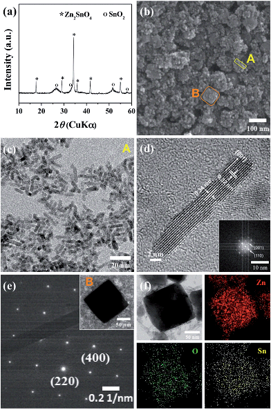 |
| | Fig. 1 Characterization of single crystalline Sn-based nanocomposites (SCSC): (a) XRD pattern, (b) SEM image, (c) low-magnification TEM image of SnO2 nanorods, (d) HRTEM image and FFT pattern of SnO2 nanorods, (e) low-magnification TEM image with corresponding SAED patterns of the synthesized ZSO nanocubes, and (f) EDS plotted area and EDS mapping of Zn (red), O (green), and Sn (yellow). | |
To further elucidate the formation process of the SCSC, a series of time-dependent experiments were performed at a fixed ratio of Zn/Sn = 1. Fig. 2 shows the XRD patterns of products prepared at various reaction times. At the initial reaction stage (30 min), XRD peaks originating from the ZnSn(OH)6 phase were identified. Particularly, its sharp peaks suggest the formation of a relatively large ZnSn(OH)6 phase. In alkali solutions, ZnSn(OH)6 is easily formed from Zn2+ and Sn4+ ions, and the rapid growth rate of metal hydroxystannate leads to a large-sized morphology in spite of the short reaction time.33 Interestingly, as the reaction time increases (90 min), the peaks corresponding to ZnSn(OH)6 disappear, whereas those corresponding to the mixture phases of ZSO and SnO2 were observed, implying that ZnSn(OH)6 was decomposed into SnO2 and ZSO.
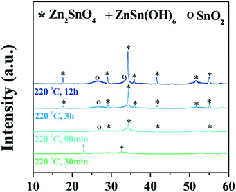 |
| | Fig. 2 XRD patterns of products obtained with different reaction times (Zn/Sn ratio = 1). | |
Generally, the formed ZnSn(OH)6 reacts with the soluble alkali species Zn(OH)42− or Sn(OH)62− in the reaction solution at a temperature ≥200 °C, which leads to the formation of either Zn2SnO4 or SnO2, respectively. At longer reaction times (3 and 12 h), the ZSO and SnO2 peaks are further enhanced, indicating the growth of oxides. The phase and morphology of Sn-based oxides prepared with different Zn/Sn ratios were investigated to understand the role of Zn ions at fixed Sn and hydrazine concentrations. Fig. 3a shows the X-ray diffraction (XRD) patterns of the products synthesized with various Zn/Sn ratios (0 ≤ Zn/Sn ≤ 2) at 220 °C for 12 h. At low Zn/Sn ratios (0 and 0.3), the pure SnO2 phase is observed, whereas an increase in the Zn/Sn ratio induces a mixed phase of SnO2 and ZSO. As mentioned above, the sharp peak pattern of ZSO is confirmed at a specific ratio (Zn/Sn = 1), suggesting a relatively large crystallite size. With a further increase to Zn/Sn = 1.8, the peaks of the ZSO are broadened, indicating the formation of small-sized particles. When the Zn/Sn ratio is 2, the pure Zn2SnO4 phase is observed. Moreover, the morphology of the products with various Zn/Sn ratios was examined via electron microscope analysis (Fig. 3b–e). In the absence of Zn cations (Zn/Sn = 0), well-dispersed spherical SnO2 NPs with ∼10 nm size are obtained (Fig. 3b). When Zn cations are introduced into the reaction solution (Zn/Sn = 0.3), a change in morphology can be induced as SnO2 nanorods reach a 2 nm width and a 15 nm length (Fig. 3c). When the Zn concentration is increased to Zn/Sn = 1, a SCSC composed of single crystalline ZSO nanocubes and SnO2 nanorods is obtained (Fig. 1). Interestingly, with a further Zn concentration increase to Zn/Sn = 1.8, a mixture of spherical ZSO NPs with a size of ∼20 nm and SnO2 nanorods is obtained (Fig. 3d). When the Zn/Sn ratio is 2, only spherical ZSO NPs with a size of ∼20 nm are observed. Based on these results, the cation ratio (Zn/Sn) plays a crucial role in the crystallization process and morphology change. On the basis of the experimental results, we propose plausible synthetic pathways for Sn-based oxides, as illustrated in Fig. 4. In a hydrazine–zinc system, Zn ions are easily coordinated by the hydrazine (i.e., consumption of hydrazine by Zn ions), and thus the concentration of free hydrazine in the reaction solution is reduced with an increase of the concentration of Zn ions, resulting in a decrease of pH in the solution.34,35 Therefore, the Zn/Sn ratio, i.e., an increase of the concentration of Zn ions in the precursor solution, plays an important role in controlling the phase and morphology of the products. In the absence of Zn ions (i.e., high concentration of free hydrazine), pure SnO2 nanoparticles (SP) are formed from Sn(OH)62− anions which are generated through the reaction of Sn4+ and OH− originating from the decomposition of hydrazine, while pure ZSO is produced when the ratio of Zn/Sn equals 2.36 The ratio of Zn/Sn of 2 facilitates the formation of Zn(N2H4)x·(OH)y with an optimum hydrazine concentration, which enables the formation of pure Zn2SnO4 nanoparticles (ZP).2 We suggest that various pathways for the formation of Sn-based oxides exist in the range of 0 < Zn/Sn < 2. In the case of Zn/Sn = 0.3 (with a relatively high free hydrazine concentration), excess Sn(OH)62− and some Zn(OH)42− anions are formed from the high OH− concentration. Under a hydrothermal reaction above 200 °C, ZnSn(OH)6 nuclei prevail due to the reaction between Sn(OH)62− and Zn(OH)42−. Then, the resultant ZnSn(OH)6 reacts with excess Sn(OH)62− and begins to decompose into Zn2xSn(1−x)O2 with preferential growth along the [001] direction, i.e., resulting in the formation of nanorods.37–39 Generally, when either NH4OH or NaOH is employed as the alkaline mineralizer, ZnSn(OH)6 nuclei rapidly grow into large particles via an aggregation mechanism and Ostwald ripening process, resulting in large aggregated products (Fig. S1†).37–39 On the other hand, in a Zn–hydrazine system with a specific Zn/Sn ratio of 0.3, the rapid growth of ZnSn(OH)6 is suppressed, resulting in small and well-dispersed SnO2 nanorods (SR). Interestingly, with increasing additional Zn concentration (Zn/Sn = 1), partial ZnSn(OH)6 nuclei grow into large particles, which react with partial Zn(OH)42− during the hydrothermal reaction40 and lead to the formation of cubic shaped ZSO with sizes of ∼100 nm. Importantly, this process controlled by the cation ratios in hydrazine considerably reduced the crystal size of the ZSO nanocubes (∼100 nm) compared to previous reports (>1 μm)23,40,41 As a result, single crystalline nanocomposite oxides composed of SnO2 nanorods and Zn2SnO4 nanocubes, called the single crystalline Sn-based nanocomposite (SCSC), were produced at Zn/Sn = 1. However, a large amount of Zn (Zn/Sn = 1.8) resulted in the formation of Sn-based nanocomposite oxides (SC) consisting of spherical ZSO NPs and SnO2 nanorods. This is attributed to the decreased concentration of OH− in the reaction solution by the reduction of free hydrazine concentration at a ratio of Zn/Sn > 1.8. A decrease in OH− concentration prefers the formation of Zn(N2H4)x·(OH)y to ZnSn(OH)6, resulting in spherical ZSO NPs with some SnO2 nanorods.
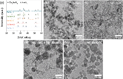 |
| | Fig. 3 (a) XRD patterns and (b–e) TEM images of the products obtained with different Zn/Sn ratios (0 ≤ Zn/Sn ≤ 2). | |
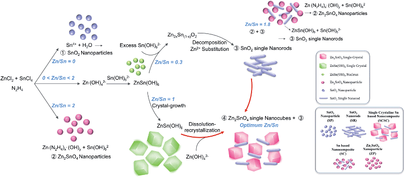 |
| | Fig. 4 Schematic illustration of the formation of the Sn-based oxides as a function of the Zn/Sn ratio. (SP: SnO2 nanoparticles, SR: SnO2 nanorods, SCSC: nanocomposite oxides composed of SnO2 nanorods and Zn2SnO4 nanocubes, SC: the nanocomposite consisting of spherical ZSO NPs and SnO2 nanorods, and ZP: Zn2SnO4 nanoparticles.) | |
Application of cation-controlled Sn-based oxides as ETLs in PSCs
To apply them as ETLs in PSCs, Sn-based oxides should be deposited in thin-layers on the substrate. As shown in Fig. S2,† most of the films deposited by spin-coating exhibit a smooth and uniform surface with densely packed NPs, while the SCSC-based film shows a rough morphology due to the relatively large ZSO nanocubes. The different morphology of Sn-based films does not affect the perovskite morphology (Fig. S3†). In addition, the cross-sectional SEM images reveal that all ETLs and perovskite films possess a uniform and dense morphology with a thickness of ∼100 nm and ∼340 nm, respectively (Fig. S4†). As shown in Fig. 5, we compared the device performance, measured under simulated solar illumination (100 mW cm−2 AM 1.5), of each Sn-based ETL. The average solar cell parameters extracted from current–voltage curves are summarized in Table 1. With an increase in the portion of ZSO (increase of Zn/Sn ratio), the average open-circuit voltage (Voc) gradually increases from 0.95 ± 0.02 to 1.04 ± 0.02 mA cm−2. This can be ascribed to the higher Vbi of ZSO than that of SnO2, and thus reduced carrier recombination between the perovskite/ETL interface, as will be shown later. The average short-circuit current density (Jsc) increases monotonically from SP to SCSC, reaching the maximum value of 22.11 ± 0.27 mA cm−2, after which it gradually decreases with an increase in the portion of ZSO (increase of Zn/Sn ratio). Interestingly, despite low temperature processing below 150 °C, the SCSC-based PSC shows the highest fill factor (FF) of 75.53 ± 1.52%, which is the main factor for the enhanced performance. The high Jsc of ≥22 mA cm−2 and FF of ≥75% for the SCSC-based PSC may be ascribed to its superior electron collection abilities (electron transport ability and reduced recombination). Owing to the combination of excellent electrical properties of SnO2 and Zn2SnO4 and their optimized morphology to reduce electron paths and recombination, the power conversion efficiency (PCE) of the SCSC exhibits the highest value of 17.5% with a steady state PCE of 16.5%.
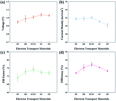 |
| | Fig. 5 Average photovoltaic properties of 5 types of ETL, SP, SR, SCSC, SC, and ZP, based PSCs (a) open-circuit voltage (Voc), (b) photocurrent density (Jsc), (c) fill factor (FF), and (d) power conversion efficiency. | |
Table 1 Average photovoltaic parameters of PSCs with different ETLs (SP, SR, SCSC, SC, and ZP)
| Sample |
V
oc (V) |
J
sc (mA cm−2) |
FF (%) |
η (%) |
| SP |
0.95 ± 0.02 |
21.77 ± 0.33 |
71.35 ± 1.95 |
14.80 ± 0.14 |
| SR |
0.99 ± 0.04 |
21.82 ± 0.48 |
74.36 ± 1.46 |
16.18 ± 0.71 |
| SCSC |
1.01 ± 0.02 |
22.11 ± 0.27 |
75.53 ± 1.52 |
16.97 ± 0.57 |
| SC |
1.04 ± 0.02 |
21.13 ± 0.21 |
73.95 ± 0.99 |
16.20 ± 0.16 |
| ZP |
1.03 ± 0.01 |
20.20 ± 0.51 |
73.68 ± 0.95 |
15.32 ± 0.25 |
To further elucidate the correlation between various Sn-based nanomaterials and cell performance, time-resolved photoluminescence (TRPL) and transient photovoltage (TPV) measurements were performed on the solar cells. Fig. 6a displays the TRPL curves of Sn-based nanomaterials/MAPbI3/PMMA. Based on the bi-exponential fitting, the obtained PL lifetimes (τavg) are 1.92 ns, 2.17 ns, 2.54 ns, 2.72 ns, and 4.18 ns for SP-, SR-, SCSC-, SC-, and ZP-based films, respectively. Compared to the MAPbI3/PMMA reference (τavg = 23.51, non-quenching sample), all the samples show more than 5 times longer lifetimes, suggesting that Sn-based oxides work well as electron collectors because of the faster charge injection process.41,42 It is notable that the PL lifetime gradually increases with a decrease in the Zn/Sn ratio. Namely, the ETLs consisting of SnO2 (SP and SR) exhibit more effective electron transfer from the perovskite to the ETL than those based on ZSO (SCSC, SC and ZP). The more efficient electron extraction in Sn-based ETLs may be associated with the higher carrier mobility or lower CB edges of SnO2 relative to ZSO.42,43 Although the nanocomposites composed of SnO2 and Zn2SnO4 (SCSC and SC) exhibit shorter PL lifetimes compared to pure SnO2 ETLs, they still have a longer PL lifetime than pure ZSO ETLs, indicating that they can operate as an effective ETL candidate. Fig. 6b shows the recombination lifetimes of Sn-based PSCs as a function of Voc. The increase in the Zn/Sn ratio i.e., the introduction of ZSO into ETLs (SCSC, SC and ZP), enhances the τn value, suggesting that ZSO-based PSCs have a much slower recombination rate than SnO2-based PSCs. Particularly, the SCSC-based PSC shows the slowest recombination rate among all devices. The reduced carrier recombination is attributed to higher built-in potential (Vbi) induced by the lower work function of ZSO relative to that of SnO2. The high Vbi is expected to lead to reduced photo-generated carrier recombination at the interface between the perovskite and ETL.44,45 Additionally, the single crystalline nanocube morphology with high crystallinity is expected to result in a lower density of recombination sites (e.g., traps) in the ETL and short electron paths compared to other counterparts, which can contribute to reduced carrier recombination in PSCs.46 Therefore, the superior electron collection of the SCSC due to superior electrical properties, enhanced Vbi, and favorable morphology can lead to the best device performance among other counterparts.
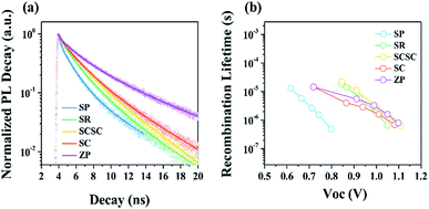 |
| | Fig. 6 (a) Time-resolved photoluminescence (TRPL) curves of quartz (Q)/SP/MAPbI3 (red), Q/SR/MAPbI3 (blue), Q/SCSC/MAPbI3 (green), Q/SC/MAPbI3 (orange), and Q/ZP/MAPbI3 (magenta). All PL is collected at 770 ± 5 nm for perovskite, and the entire sample is excited by a picosecond diode laser of 670 nm. (b) Measured photoinduced transient photovoltage (TPV) decays of 5 types of ETL, SP, SR, SCSC, SC, and ZP, based PSCs at 100 mW cm−2. | |
To demonstrate the potential of the SCSC as an alternative to TiO2, especially in a low temperature annealed process, we compared the device performance of SCSC-based PSCs with that of TiO2-based PSCs (TiO2 layer was also annealed at low temperature below 150 °C). For clear comparison, no effort was made to improve PSC performance (we didn't perform perovskite and ETL optimization). Fig. 7a exhibits photocurrent density–voltage (J–V) characteristics of the SCSC- and TiO2-based PSCs and their average solar cell parameters are added in Fig. S5 and Table S1.† It is noteworthy that the SCSC-based PSC (Jsc of 22 mA cm−2, Voc of 1.03 V, a FF of 75.3% and a PCE of 17.2% with a stabilized PCE of 16.5%) exhibits better photovoltaic performance than the TiO2-based counterpart (Jsc of 20.6 mA cm−2, Voc of 1.03 V, FF of 71.0% and a PCE of 15.2% with the stabilized PCE of 14.3%) (Fig. S6†). Although our group have achieved the record efficiency over 22% with high temperature processed mesoporous TiO2 , in the case of low temperature processing, the TiO2 nanoparticle film-based planar PSCs still show inferior performance without additional optimization processes (perovskite composition engineering, interface engineering, and nanoparticle engineering) due to their poor electrical (no necking between particles) and optical properties.13,30,47 However, in spite of low temperature processing, the SCSC-based PSCs achieved a superior device performance of ≥17% due to their comparable Jsc and FF with high temperature processed PSCs. Furthermore, the external quantum efficiency (EQE) of the SCSC-based PSC is almost 10% higher than that of the TiO2-based PSC, which is consistent with the Jsc trend (Fig. 7b). These differences in photovoltaic properties originate from the different light (light harvesting) and charge management abilities (charge collection) of the ETLs. Fig. 7c presents the transmittance and diffuse reflectance spectra of the TiO2/ITO and SCSC/ITO substrates. The introduction of the SCSC leads to a significant improvement in transmittance even compared to the ITO substrate due to the reduced reflectance over the entire wavelength region, while the TiO2 exhibits a reduction of transmittance due to higher reflectance. Typically, Sn-based materials (e.g., SnO2 and ZSO) have a relatively low reflective index (n < 2) compared to TiO2 (n = 2.5). The lower reflective index of the SCSC than that of TiO2 minimizes the light loss induced at the interface due to the anti-reflection effect, which improves light transmittance.2,13 More importantly, to evaluate the light management ability of a device, the light harvesting efficiency (LHE) of the SCSC and TiO2 film with a perovskite absorber was compared using absorption (A) and reflection spectra (R) with the following equation: LHE = (1 − R)(1 − 10−A).48,49 As shown in Fig. 7d, the LHE of the SCSC-based PSC is slightly higher than that of the TiO2-based PSC, which means that the transparent SCSC film uses incident light more efficiently than the TiO2 film, and thus increases the absorption of the perovskite film. Moreover, to confirm the charge collection ability of the devices, the internal quantum efficiency (IQE) was calculated based on EQE and LHE (Fig. 7e).49 Since the IQE excludes the light harvesting term, it only indicates the charge collection of devices. The calculated IQE of the SCSC-based PSC is greater than that of the devices based on TiO2 between 400 nm and 750 nm, demonstrating the superior charge collecting properties of the SCSC.50 The greater IQE is attributed to the improved electron mobility due to the single crystalline nature of the SCSC. Its advantages in PSCs are schematically outlined in Fig. 7f. The improved light and charge collecting management abilities of the SCSC make it an exceptional alternative to TiO2 as an ETL in low temperature processed PSCs.
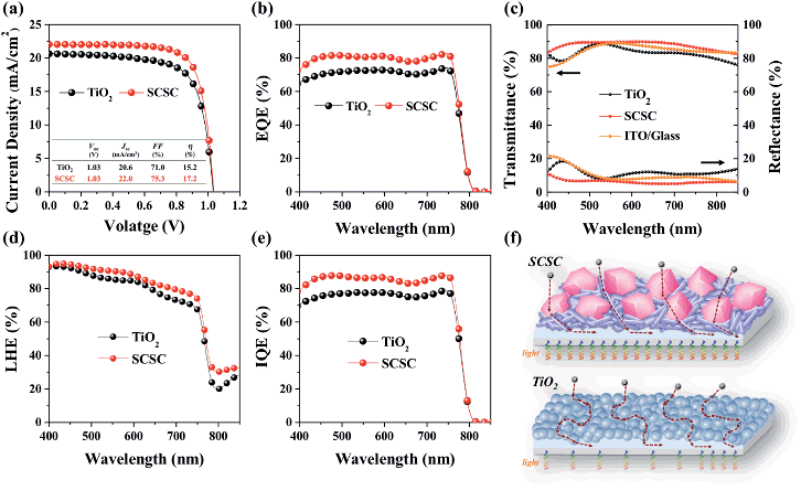 |
| | Fig. 7 Comparison of TiO2 NP-based PSCs vs. SCSC-based PSCs: (a) the representative current density–voltage (J–V) characteristics of the TiO2-based device (black) and SCSC-based device (red) measured by reverse scan with a 10 mV voltage step and 40 ms delay time under simulated AM 1.5 G 100 mW cm−2 illumination. The photovoltaic parameters are summarized in the inset; (b) EQE spectra of the TiO2-based PSCs and SCSC-based PSCs; (c) transmittance and reflectance spectra of ITO/TiO2, ITO/SCSC, and bare ITO substrates; (d) LHE and (e) IQE of the TiO2-based PSCs and SCSC-based PSCs, and (f) schematic illustration of the comparison of TiO2 NP- and SCSC-based PSCs based on their carrier and light management characteristics. | |
Conclusions
In summary, a SCSC consisting of SnO2 nanorods and ZSO nanocubes was successfully synthesized via a facile hydrazine-assisted hydrothermal method. We found that the control of the cation ratio (Zn/Sn) with hydrazine as a complexing agent and an alkaline mineralizer affects the intermediate phase and growth kinetics during the reaction, resulting in the formation of various Sn-based materials. The specific cation ratio of Zn/Sn = 1 led to the formation of the SCSC. Based on controlled experiments, we proposed the possible synthesis mechanism. To compare their photovoltaic performance, the synthesized Sn-based materials were employed as ETLs in low temperature processed PSCs. Among them, the SCSC-based PSCs exhibited the most excellent device performance exceeding 17% due to their superior charge collecting properties. Furthermore, the device performance of SCSC-based PSCs was compared with that of TiO2-based PSCs to demonstrate that the SCSC is an exceptional alternative to TiO2. Quantum efficiency analyses reveal that the SCSC-based PSCs possess superior light harvesting and charge collecting efficiency relative to TiO2-based PSCs, leading to a better device performance. Our findings provide an effective solution for the synthesis of single crystalline Sn-based nanomaterials, which can pave the way to further improve the energy conversion efficiency and stability of alternatives to TiO2 in PSCs.
Acknowledgements
This work was supported by the National Research Foundation of Korea (NRF) grants funded by the Ministry of Science, ICT & Future Planning (MSIP) of Korea under contract number. NRF-2011-0031565 (Global Frontier R&D Program for Multiscale Energy System), and NRF-2015M1A2A2056542 (climate change program), and NRF-2016R1A5A1009926 (Wearable platform Materials Technology Center: ERC program). This work was also supported by the KRICT-SKKU DRC program.
Notes and references
- Z. Wang, J. Liu, F. Wang, S. Chen, H. Luo and X. Yu, J. Phys. Chem. C, 2010, 114, 13577–13582 Search PubMed.
- S. S. Shin, W. S. Yang, J. H. Noh, J. H. Suk, N. J. Jeon, J. H. Park, J. S. Kim, W. M. Seong and S. I. Seok, Nat. Commun., 2015, 6, 7410 Search PubMed.
- E. N. Dattoli, Q. Wan, W. Guo, Y. Chen, X. Pan and W. Lu, Nano Lett., 2007, 7, 2463–2469 Search PubMed.
- M. Ohtaki, H. Koga, T. Tokunaga, K. Eguchi and H. Arai, J. Solid State Chem., 1995, 120, 105–111 Search PubMed.
- H. J. Snaith and C. Ducati, Nano Lett., 2010, 10, 1259–1265 Search PubMed.
- H. Mizoguchi, P. Chen, P. Boolchand, V. Ksenofontov, C. Felser, P. W. Barnes and P. M. Woodward, Chem. Mater., 2013, 25, 3858–3866 Search PubMed.
- T. Kawabe, K. Tabata, E. Suzuki, Y. Yamaguchi and Y. Nagasawa, J. Phys. Chem. B, 2001, 105, 4239–4244 Search PubMed.
- M. Sinner-Hettenbach, N. Barsan, U. Weimar, T. Weiss, H. Von Schenck, M. Göthelid, L. Giovanelli and G. Le Lay, Thin Solid Films, 2001, 391, 192–197 Search PubMed.
- X. Dou, D. Sabba, N. Mathews, L. H. Wong, Y. M. Lam and S. Mhaisalkar, Chem. Mater., 2011, 23, 3938–3945 CrossRef CAS.
- A. Bera, K. Wu, A. Sheikh, E. Alarousu, O. F. Mohammed and T. Wu, J. Phys. Chem. C, 2014, 118, 28494–28501 Search PubMed.
- H. S. Rao, B. X. Chen, W. G. Li, Y. F. Xu, H. Y. Chen, D. B. Kuang and C. Y. Su, Adv. Funct. Mater., 2015, 25, 7200–7207 Search PubMed.
- Z. Zhu, J. Ma, Z. Wang, C. Mu, Z. Fan, L. Du, Y. Bai, L. Fan, H. Yan and D. L. Phillips, J. Am. Chem. Soc., 2014, 136, 3760–3763 Search PubMed.
- W. Ke, G. Fang, Q. Liu, L. Xiong, P. Qin, H. Tao, J. Wang, H. Lei, B. Li and J. Wan, J. Am. Chem. Soc., 2015, 137, 6730–6733 Search PubMed.
- J. P. C. Baena, L. Steier, W. Tress, M. Saliba, S. Neutzner, T. Matsui, F. Giordano, T. J. Jacobsson, A. R. S. Kandada and S. M. Zakeeruddin, Energy Environ. Sci., 2015, 8, 2928–2934 Search PubMed.
- X. Feng, K. Zhu, A. J. Frank, C. A. Grimes and T. E. Mallouk, Angew. Chem., 2012, 124, 2781–2784 Search PubMed.
- E. J. Crossland, N. Noel, V. Sivaram, T. Leijtens, J. A. Alexander-Webber and H. J. Snaith, Nature, 2013, 495, 215–219 Search PubMed.
- P. Archana, R. Jose, C. Vijila and S. Ramakrishna, J. Phys. Chem. C, 2009, 113, 21538–21542 Search PubMed.
- T. Lana-Villarreal, G. Boschloo and A. Hagfeldt, J. Phys. Chem. C, 2007, 111, 5549–5556 CAS.
- J. T.-W. Wang, J. M. Ball, E. M. Barea, A. Abate, J. A. Alexander-Webber, J. Huang, M. Saliba, I. n. Mora-Sero, J. Bisquert and H. J. Snaith, Nano Lett., 2013, 14, 724–730 Search PubMed.
- Y. Sun, J. H. Seo, C. J. Takacs, J. Seifter and A. J. Heeger, Adv. Mater., 2011, 23, 1679–1683 Search PubMed.
- L. Qin, J. Xu, X. Dong, Q. Pan, Z. Cheng, Q. Xiang and F. Li, Nanotechnology, 2008, 19, 185705 Search PubMed.
- H. Fan, Z. Liu, J. Yang, C. Wei, J. Zhang, L. Wu and W. Zheng, RSC Adv., 2014, 4, 49806–49810 Search PubMed.
- M. H. Al-Hinai, A. T. Al-Hinai and J. Dutta, J. Mater. Sci., 2014, 49, 7282–7289 Search PubMed.
- Y. Zhang, M. Guo, M. Zhang, C. Yang, T. Ma and X. Wang, J. Cryst. Growth, 2007, 308, 99–104 Search PubMed.
- M. Miyauchi, Z. Liu, Z.-G. Zhao, S. Anandan and K. Hara, Chem. Commun., 2010, 46, 1529–1531 Search PubMed.
- Y. Bai, H. Yu, Z. Li, R. Amal, G. Q. M. Lu and L. Wang, Adv. Mater., 2012, 24, 5850–5856 Search PubMed.
- W. J. Moon, J. H. Yu and G. M. Choi, Sens. Actuators, B, 2001, 80, 21–27 Search PubMed.
- J. Song, E. Zheng, X.-F. Wang, W. Tian and T. Miyasaka, Sol. Energy Mater. Sol. Cells, 2016, 144, 623–630 Search PubMed.
- D. Liu and T. L. Kelly, Nat. Photonics, 2014, 8, 133–138 CrossRef CAS.
- T. Leijtens, G. E. Eperon, S. Pathak, A. Abate, M. M. Lee and H. J. Snaith, Nat. Commun., 2013, 4, 2761 Search PubMed.
- L. Vayssieres and M. Graetzel, Angew. Chem., 2004, 116, 3752–3756 Search PubMed.
- E. Leite, T. Giraldi, F. Pontes, E. Longo, A. Beltran and J. Andres, Appl. Phys. Lett., 2003, 83, 1566–1568 CrossRef CAS.
- S. Baruah and J. Dutta, Sci. Technol. Adv. Mater., 2011, 12, 013004 CrossRef PubMed.
- H. Zhu, D. Yang, G. Yu, H. Zhang and K. Yao, Nanotechnology, 2006, 17, 2386 Search PubMed.
- B. T. Heaton, C. Jacob and P. Page, Coord. Chem. Rev., 1996, 154, 193–229 Search PubMed.
- K. Jain, A. Shrivastava and R. Rashmi, ECS Trans., 2006, 1, 1–7 Search PubMed.
- Z. Chen, M. Cao and C. Hu, J. Phys. Chem. C, 2011, 115, 5522–5529 Search PubMed.
- Z. Li, X. Li, X. Zhang and Y. Qian, J. Cryst. Growth, 2006, 291, 258–261 Search PubMed.
- X. Ding, D. Zeng and C. Xie, Sens. Actuators, B, 2010, 149, 336–344 CrossRef CAS.
- J. Zeng, M. Xin, K. Li, H. Wang, H. Yan and W. Zhang, J. Phys. Chem. C, 2008, 112, 4159–4167 Search PubMed.
- Y.-Q. Jiang, C.-X. He, R. Sun, Z.-X. Xie and L.-S. Zheng, Mater. Chem. Phys., 2012, 136, 698–704 Search PubMed.
- O. Gunawan, T. K. Todorov and D. B. Mitzi, Appl. Phys. Lett., 2010, 97, 3506 Search PubMed.
- C. S. Ponseca Jr, T. J. Savenije, M. Abdellah, K. Zheng, A. Yartsev, T. r. Pascher, T. Harlang, P. Chabera, T. Pullerits and A. Stepanov, J. Am. Chem. Soc., 2014, 136, 5189–5192 Search PubMed.
- W. A. Laban and L. Etgar, Energy Environ. Sci., 2013, 6, 3249–3253 Search PubMed.
- M. Hu, L. Liu, A. Mei, Y. Yang, T. Liu and H. Han, J. Mater. Chem. A, 2014, 2, 17115–17121 Search PubMed.
- Q. Shen, Y. Ogomi, J. Chang, S. Tsukamoto, K. Kukihara, T. Oshima, N. Osada, K. Yoshino, K. Katayama and T. Toyoda, Phys. Chem. Chem. Phys., 2014, 16, 19984–19992 Search PubMed.
- P. Tiwana, P. Docampo, M. B. Johnston, H. J. Snaith and L. M. Herz, ACS Nano, 2011, 5, 5158–5166 Search PubMed.
- A. G. Agrios and A. Hagfeldt, J. Mater. Chem. C, 2008, 112, 10021–10026 Search PubMed.
- Q. Lin, A. Armin, R. C. R. Nagiri, P. L. Burn and P. Meredith, Nat. Photonics, 2015, 9, 106–112 Search PubMed.
- D. H. Kim, G. S. Han, W. M. Seong, J. W. Lee, B. J. Kim, N. G. Park, K. S. Hong, S. Lee and H. S. Jung, ChemSusChem, 2015, 8, 2392–2398 Search PubMed.
Footnotes |
| † Electronic supplementary information (ESI) available: SEM image of Zn doped SnO2 synthesized using NaOH as the OH− supplier instead of N2H4 under the low Zn/Sn molar ratio conditions (Fig. S1), plane-view SEM images of tin-based nanostructure films on fused silica substrates (Fig. S2), plane-view SEM images of perovskite/ETL films on fused silica substrates (Fig. S3), cross-sectional SEM images of perovskite/ETL films on fused silica substrates (Fig. S4), average photovoltaic properties of TiO2- and SCSC-based PSCs (Fig. S4), the stabilized power conversion efficiency of SCSC-based and TiO2-based PSCs at the maximum power point (Fig. S5), and average photovoltaic parameters of TiO2- and SCSC-based PSCs (Table S1). See DOI: 10.1039/c6ta08565b |
| ‡ These authors contributed equally to this work. |
|
| This journal is © The Royal Society of Chemistry 2017 |
Click here to see how this site uses Cookies. View our privacy policy here. 
 *b and
Sang Il
Seok
*ad
*b and
Sang Il
Seok
*ad


